

Page 1
STN2NF10
N-CHANNEL 100V - 0.23Ω - 2A SOT-223
STripFET™ II POWER MOSFET
TYPE
V
DSS
STN2NF10 100 V < 0.26
■ TYPICAL R
(on) = 0.23 Ω
DS
R
DS(on)
I
D
Ω
2 A
DESCRIPTION
This Power MOSFET is the latest dev elo pment of
STMicroelectronis unique "Single Feature Size™"
strip-based process. The resulting transistor
shows extremely high packing density for low onresistance, rugged avalanche characteristics and
less critical alignment steps therefore a remarkable manufacturing reproducibility.
APPLICATIONS
■ DC-DC & DC-AC COVERTERS
■ DC MOTOR CONTROL (DISK DRIVERS, etc.)
■ SYNCHRONOUS RECTIFICATION
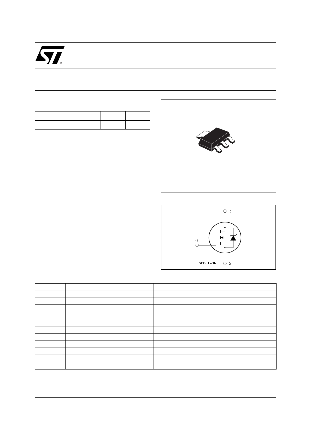
2
3
2
1
SOT-223
INTERNAL SCHEMATIC DIAGRAM
ABSOLUTE MAXIMUM RATINGS
Symbol Parameter Value Unit
V
DS
V
DGR
V
GS
(
I
•)
D
I
D
(
I
••)
DM
P
tot
(1)
E
AS
T
stg
T
j
(
Pulse wi dth limited by safe operating area.
••)
(
Current limited by the package
•)
.
Drain-source Voltage (VGS = 0)
Drain-gate Voltage (RGS = 20 kΩ)
100 V
100 V
Gate- source Voltage ± 20 V
Drain Current (continuos) at TC = 25°C
Drain Current (continuos) at TC = 100°C
2A
1.26 A
Drain Current (pulsed) 8 A
Total Dissipation at TC = 25°C
2.5 W
Derating Factor 0.02 W/°C
Single Pulse Avalanche Energy 300 mJ
Storage Temperature -65 to 150 °C
Max. Operating Junction Temperature 150 °C
≤1A, di/dt ≤300A/µs , VDD ≤ V
(1) I
SD
(BR)DSS
, Tj ≤ T
JMAX
1/8December 2001
Page 2
STN2NF10
THERMA L D ATA
Rthj-pcb
Rthj-pcb
T
Thermal Resistance Junction-PCB
(1 inch
Thermal Resistance Junction-PCB (min. footprint)
Maximum Lead Temperature For Soldering Purpose
l
2
copper board)
Typ
50
90
260
°C/W
°C/W
°C
ELECTRICAL CHARACTERISTICS (T
= 25 °C unless otherwise specified)
case
OFF
Symbol Parameter Test Conditions Min. Typ. Max. Unit
I
= 250 µA, VGS = 0
D
V
= Max Rating
DS
V
= Max Rating TC = 125°C
DS
= ± 20V
V
GS
100 V
1
10
±100 nA
ON
V
(BR)DSS
I
DSS
I
GSS
(1)
Drain-source
Breakdown Voltage
Zero Gate Voltage
Drain Current (V
GS
Gate-body Leakage
Current (V
DS
= 0)
= 0)
Symbol Parameter Test Conditions Min. Typ. Max. Unit
V
V
GS(th)
R
DS(on)
Gate Threshold Voltage
Static Drain-source On
Resistance
= VGS I
DS
V
= 10 V ID = 1 A
GS
= 250 µA
D
24V
0.23 0.26
DYNAMIC
Symbol Parameter Test Conditions Min. Typ. Max. Unit
(*)
g
fs
C
iss
C
oss
C
rss
Forward Transconductance
Input Capacitance
Output Capacitance
Reverse Transfer
Capacitance
V
DS>ID(on)xRDS(on)max ID
= 25V, f = 1 MHz, VGS = 0
V
DS
=1A
2.5 S
280
45
20
µA
µA
Ω
pF
pF
pF
2/8
Page 3
STN2NF10
ELECTRICAL CHARACTERISTICS (continued)
SWITCHING ON
Symbol Parameter Test Conditions Min. Typ. Max. Unit
= 50 V ID = 1 A
t
d(on)
Turn-on Delay Time
t
r
Rise Time
V
DD
R
= 4.7 Ω VGS = 10 V
G
(Resistive Load, Figure 3)
Q
g
Q
gs
Q
gd
Total Gate Charge
Gate-Source Charge
Gate-Drain Charge
= 80V ID= 2A VGS=10V
V
DD
SWITCHING OFF
Symbol Parameter Test Conditions Min. Typ. Max. Unit
t
d(Voff)
t
t
Turn-off Delay Time
f
c
Fall Time
Cross-over Time
= 80 V ID = 2 A
V
clamp
R
= 4.7Ω, V
G
GS
= 10 V
(Inductive Load, Figure 5)
SOURCE DRAIN DIODE
Symbol Parameter Test Conditions Min. Typ. Max. Unit
I
SD
I
SDM
V
SD
t
rr
Q
rr
I
RRM
(*)
Pulsed: P ul se duration = 300 µs, duty cycle 1.5 %.
(
•)Pulse width limited by s afe operating area.
Source-drain Current
(•)
Source-drain Current (pulsed)
(*)
Forward On Voltage
Reverse Recovery Time
Reverse Recovery Charge
Reverse Recovery Current
I
= 2 A VGS = 0
SD
= 2 A di/dt = 100A/µs
I
SD
V
= 10 V Tj = 150°C
DD
(see test circuit, Figure 5)
6
10
10
2.5
4
19
4
15
2
8
1.2 V
70
175
5
ns
ns
nC
nC
nC
ns
ns
ns
A
A
ns
nC
A
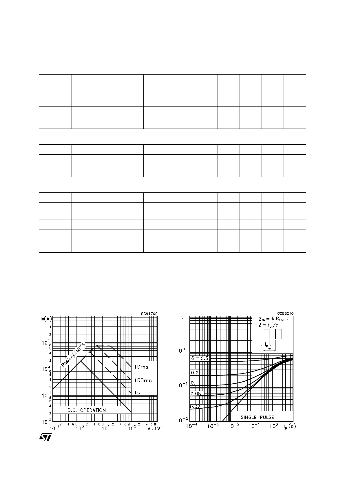
Safe Operating Area
Thermal Impedance
3/8
Page 4

STN2NF10
Output Characteristics Transfer Characteristics
Transconductance Static Drain-source On Resistance
Gate Charge vs Gate-source Voltage Capacitance Variations
4/8
Page 5

Normalized Gate Threshold Voltage vs Temperature Normalized on Resistance vs Temperature
Source-drain Diode Forward Characteristics .
STN2NF10
. .
5/8
Page 6

STN2NF10
Fig. 1: Unclamped Inductive Load Test CircuitFig. 1: Unclamped Inductive Load Test Circuit Fig. 2: Unclamped Inductive Waveform
Fig. 3: Switching Times Test Circuits For Resistive
Load
Fig. 5: Test Circuit For Inductive Load Switching
And Diode Recovery Times
Fig. 4: Gate Charge test Circuit
6/8
Page 7

SOT-223 MECHANICAL DATA
STN2NF10
DIM.
MIN. TYP. MAX. MIN. TYP. MAX.
a 2.27 2.3 2.33 89.4 90.6 91.7
b 4.57 4.6 4.63 179.9 181.1 182.3
c 0.2 0.4 0.6 7.9 15.7 23.6
d 0.630.650.6724.825.626.4
e1 1.5 1.6 1.7 59.1 63 66.9
e4 0.32 12.6
f 2.9 3 3.1 114.2 118.1 122.1
g 0.67 0.7 0.73 26.4 27.6 28.7
l1 6.7 7 7.3 263.8 275.6 287.4
l2 3.5 3.5 3.7 137.8 137.8 145.7
L 6.3 6.5 6.7 248 255.9 263.8
mm mils
l1
e1
L
a
b
f
C
B
C
E
g
d
l2
c
e4
P008B
7/8
Page 8

STN2NF10
Information furnished is believed to be accurate and reliable. However, STMicroelectronics assumes no responsibility for the consequences
of use of such information nor for any infringement of patents or other rights of third parties which may result from its use. No license is granted
by implic ation or otherwise under any patent or patent r i ght s of STMi croelectr oni cs. Spec i fications mentioned i n this publication are subject
to change without notice. This publication supersedes and replaces all information previously supplied. STMicroelectronics product s are not
authorized for use as cri tical comp onents in lif e support devi ces or systems without express written approva l of STMicroe l ectronics.
The ST logo is registered trademark of STMicroelectronics
2001 STMi croelectronics - All Ri ghts Rese rved
All other na m es are the property of their respective owners.
Australi a - Brazil - Canada - Chin a - F i nland - France - German y - Hong Kong - I ndia - Israel - It al y - Japan - Malaysia - Mal ta - Morocco -
Singap ore - Spain - Sw eden - Switzerland - Uni ted Kingdom - United St at es.
STMicroelectronics GROUP OF COMPANIES
http:// www.st.com
8/8
 Loading...