

Page 1
STN2NF06
N - CHANNEL 60V - 0.12Ω - 2A - SOT-223
STripFET POWER MOSFET
TYPE V
DSS
R
DS(on)
I
D
STN2NF06 60 V < 0.15 Ω 2A
■ TYPICALR
■ EXCEPTIONAL dv/dt CAPABILITY
■ AVALANCHERUGGEDTECHNOLOGY
■ 100 % AVALANCHETESTED
■ APPLICATIONORIENTED
DS(on)
=0.12 Ω
CHARACTERIZATION
DESCRIPTION
This Power Mosfet is the latest development of
STMicroelectronics unique ”Single Feature
Size” stip-based process. The resultingtransistor showsextremely high packing density for low
on-resistance, rugged avalanche characteristics
and less critical alignment steps therefore a remarkablemanufacturingreproducibility.
APPLICATIONS
■ DC MOTOR CONTROL (DISKDRIVES,etc.)
■ DC-DC& DC-AC CONVERTERS
■ SYNCHRONOUS RECTIFICATION
2
3
2
1
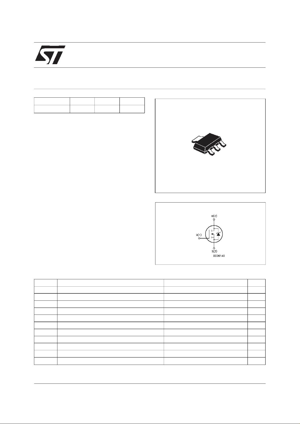
SOT-223
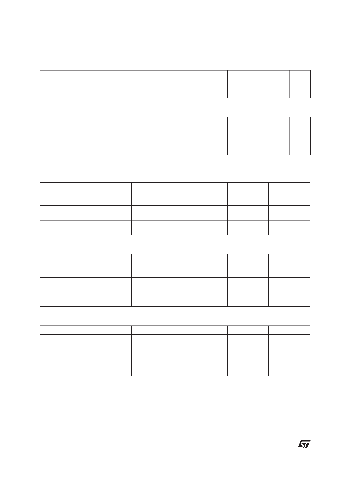
INTERNAL SCHEMATIC DIAGRAM
ABSOLUTE MAXIMUM RATINGS
Symbol Parameter Value Unit
V
V
V
I
DM
P
dv/ dt(
T
(•) Pulse width limited by safe operating area (1)ISD≤ 8A,di/dt ≤ 200 A/µs, VDD≤ V
New RDS (on) spec. starting from JULY 98
July 1998
Drain-sou rc e Volt ag e (VGS=0) 60 V
DS
DGR Drain- gate Voltage (R
Gate- source Voltage ± 20 V
GS
Drain Curre n t (continuous ) at Tc=25oC2A
I
D
I
Drain Curre n t (continuous ) at Tc=100oC 1.8 A
D
=20kΩ)
GS
60 V
(•) Drain Current (pulsed) 8 A
Total Dissipation at Tc=25oC 2.5 W
tot
Derating Fac tor 0.02 W/
1) Peak Diode Re covery volt age s lope 6 V/ns
St orage Te m peratu re -65 to 15 0
stg
Max. Operatin g Ju nction Tempe rature 150
T
j
(BR)DSS,Tj≤TJMAX
o
C
o
C
o
C
1/9
Page 2
STN2NF06
THERMAL DATA
R
thj-pcb
R
thj- amb
T
AVALANCHE CHARACTERISTICS
Symbol Para met e r Max Valu e Uni t
I
AR
E
Ther mal Resist ance Junctio n- PC Board Max
Ther mal Resist ance Junctio n- ambient Max
(Sur f a ce M ounted)
Maximum Lead T em per a t ure For Soldering P urpose
l
Avalanch e C ur rent, R ep et it i v e o r Not- Re petit ive
(pulse w idth limited b y T
Single Pulse Avalanche Energy
AS
(starting T
=25oC, ID=IAR,VDD=25V)
j
max)
j
50
60
260
2A
20 mJ
o
C/W
o
C/W
o
C
ELECTRICAL CHARACTERISTICS (T
=25oC unlessotherwisespecified)
case
OFF
Symbol Parameter Test Condition s Min. Typ. Max. Un it
V
(BR)DSS
Drain-sou rc e
=250µAVGS=0
I
D
60 V
Breakdown Voltage
I
I
DSS
GSS
Zer o G at e Voltage
Drain Curre nt ( V
GS
Gat e-body Le ak a ge
Current (V
DS
=0)
=0)
V
=MaxRating
DS
=MaxRating Tc=125oC
V
DS
= ± 20 V
V
GS
1
10
± 100 nA
ON (∗)
Symbol Parameter Test Condition s Min. Typ. Max. Un it
V
GS(th )
Gate Threshold
V
DS=VGSID
=250µA
234V
Voltage
R
DS(on)
Stati c Drain-so urce O n
VGS=10V ID=6A 0.12 0.15 Ω
Resistance
I
D(on)
On S tate Dra in Curr e nt VDS>I
D(on)xRDS(on)max
2A
VGS=10V
DYNAMIC
Symbol Parameter Test Condition s Min. Typ. Max. Un it
g
(∗)Forward
fs
Tr anscond uctanc e
C
C
C
Input Ca pac i t an c e
iss
Out put C apa c itanc e
oss
Reverse T ransfer
rss
Capa cit an c e
VDS>I
D(on)xRDS(on)maxID
=1A 1 3 S
VDS=25V f=1MHz VGS= 0 V 760
100
30
µA
µA
pF
pF
pF
2/9
Page 3
STN2NF06
ELECTRICAL CHARACTERISTICS (continued)
SWITCHINGON
Symbol Parameter Test Condition s Min. Typ. Max. Un it
t
d(on)
(di/dt)
Q
Q
Q
Turn-on Tim e
Rise T ime
t
r
Turn-on Current Slope VDD=25V ID=6A
on
Total Gate Charge
g
Gat e-Sou rc e Charge
gs
Gate-Drain Charge
gd
VDD=30V ID=6A
=4.7 Ω VGS=10V
R
G
=4.7 Ω VGS=10V
R
G
VDD=40V ID=12A VGS=10V 20
SWITCHINGOFF
Symbol Parameter Test Condition s Min. Typ. Max. Un it
t
r(Voff)
t
Of f - voltag e Ris e Time
t
Fall Time
f
Cross-over Time
c
VDD=48V ID=12A
=4.7 Ω VGS=10V
R
G
SOURCE DRAIN DIODE
Symbol Parameter Test Condition s Min. Typ. Max. Un it
I
SD
I
SDM
V
SD
t
Q
I
RRM
(∗) Pulsed: Pulse duration =300 µs, duty cycle1.5 %
(•) Pulse width limited by safe operating area
Source-drain Cu rrent
(•)
Source-drain Cu rrent
(pulsed)
(∗) F orwar d O n V o lt age ISD=2A VGS=0 1.5 V
Reverse R ecovery
rr
Time
Reverse R ecovery
rr
= 12 A di/dt = 100 A/µs
I
SD
=30V Tj=150oC
V
DD
Charge
Reverse R ecovery
Current
10
35
200 A/µ s
5
7
7
18
30
2
8
65
0.18
5.5
ns
ns
nC
nC
nC
ns
ns
ns
A
A
ns
µC
A
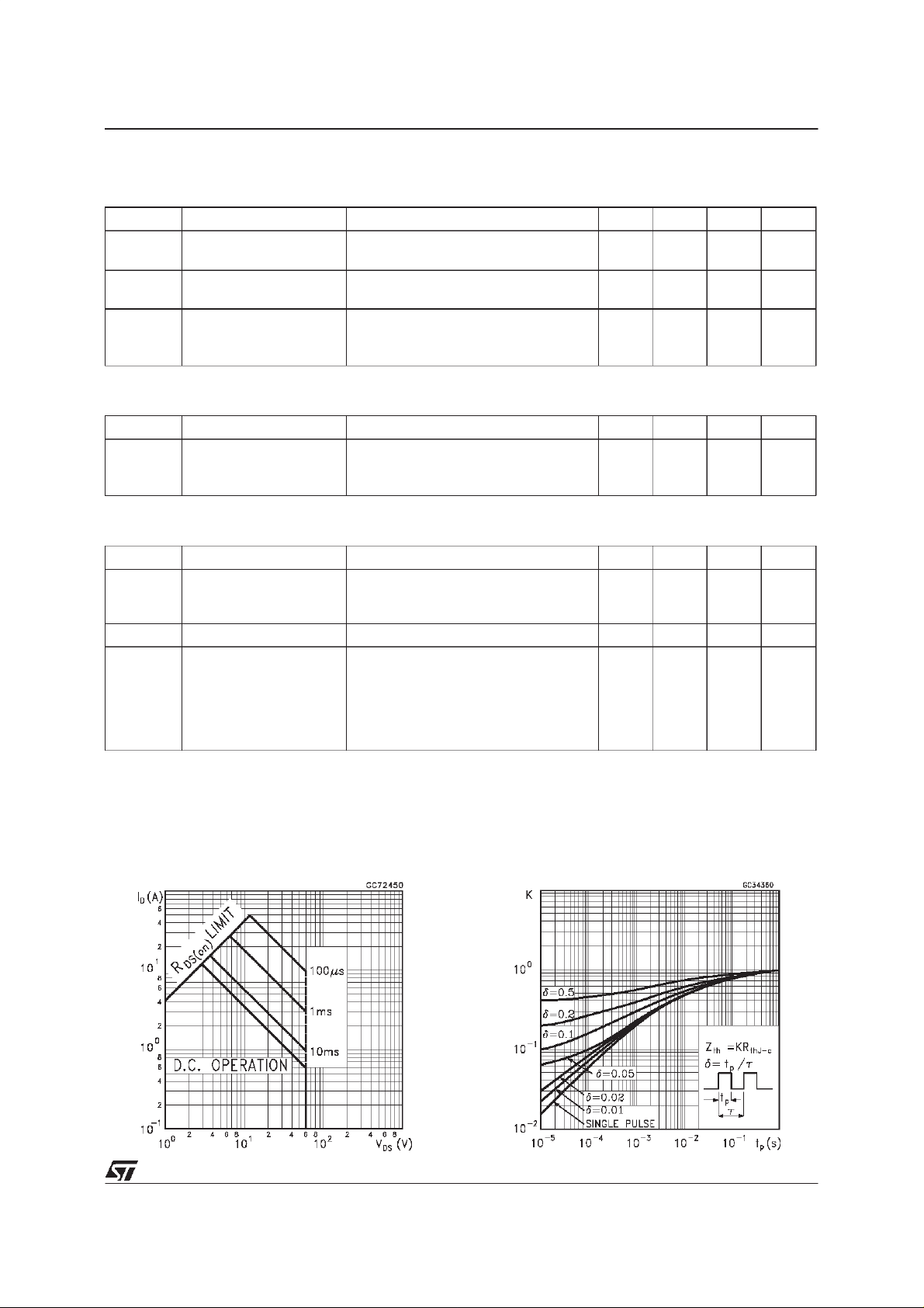
Safe Operating Area ThermalImpedance
3/9
Page 4

STN2NF06
Derating Curve
TransferCharacteristics
OutputCharacteristics
Transconductance
StaticDrain-source On Resistance
4/9
Gate Charge vs Gate-sourceVoltage
Page 5

STN2NF06
CapacitanceVariations
Normalized On Resistance vs Temperature
Normalized Gate ThresholdVoltage vs
Temperature
Turn-onCurrent Slope
Turn-offDrain-source VoltageSlope
Cross-overTime
5/9
Page 6

STN2NF06
SwitchingSafe OperatingArea
Source-drainDiode Forward Characteristics
AccidentalOverloadArea
Fig. 1: Unclamped InductiveLoad Test Circuit
6/9
Fig. 2: UnclampedInductiveWaveform
Page 7

STN2NF06
Fig. 3: SwitchingTimes Test Circuits For
ResistiveLoad
Fig. 5: Test Circuit For InductiveLoad Switching
And DIodeRecovery Times
Fig. 4: GateChargetest Circuit
7/9
Page 8

STN2NF06
SOT-223 MECHANICALDATA
DIM.
MIN. TYP. MAX. MIN. TYP. MAX.
a 2.27 2.3 2.33 89.4 90.6 91.7
b 4.57 4.6 4.63 179.9 181.1 182.3
c 0.2 0.4 0.6 7.9 15.7 23.6
d 0.63 0.65 0.67 24.8 25.6 26.4
e1 1.5 1.6 1.7 59.1 63 66.9
e4 0.32 12.6
f 2.9 3 3.1 114.2 118.1 122.1
g 0.67 0.7 0.73 26.4 27.6 28.7
l1 6.7 7 7.3 263.8 275.6 287.4
l2 3.5 3.5 3.7 137.8 137.8 145.7
L 6.3 6.5 6.7 248 255.9 263.8
mm mils
L
e1
a
b
f
C
l1
B
C
E
g
d
l2
c
e4
P008B
8/9
Page 9

STN2NF06
Information furnished is believed tobe accurate and reliable. However,STMicroelectronics assumes no responsibility for theconsequences
of use of such information nor for any infringement of patents or other rights of third parties which may result from its use. No license is
granted by implication orotherwise under any patent or patent rights of STMicroelectronics. Specification mentioned in this publication are
subject tochange withoutnotice. This publication supersedes andreplaces all information previously supplied. STMicroelectronics products
are not authorized for use as critical componentsin lifesupport devices orsystems withoutexpress written approval of STMicroelectronics.
Australia -Brazil - Canada- China - France- Germany- Italy- Japan - Korea - Malaysia - Malta- Mexico- Morocco- The Netherlands-
Singapore- Spain- Sweden - Switzerland- Taiwan-Thailand - United Kingdom- U.S.A.
The ST logo isa trademarkof STMicroelectronics
1998 STMicroelectronics– Printed in Italy – AllRights Reserved
STMicroelectronicsGROUP OF COMPANIES
.
9/9
 Loading...