

Page 1
STN2NE06
N-CHANNEL 60V - 0.18Ω - 2A - SOT-223
STripFET POWER MOSFET
TYPE V
DSS
R
DS(on)
I
D
ST N2NE06 60 V < 0 . 25 Ω 2A
■ TYPICALR
■ EXCEPTIONALdv/dtCAPABILITY
■ AVALANCHERUGGEDTECHNOLOGY
■ 100 % AVALANCHETESTED
■ APPLICATIONORIENTED
DS(on)
= 0.18 Ω
CHARACTERIZATION
DESCRIPTION
This Power Mosfet is the latest development of
STMicroelectronics unique ”Single Feature
Size” stip-based process. The resulting transi-
stor shows extremely high packing density forlow
on-resistance, rugged avalanche characteristics
and less critical alignment steps therefore a remarkablemanufacturingreproducibility.
APPLICATIONS
■ DC MOTOR CONTROL(DISK DRIVES,etc.)
■ DC-DC& DC-AC CONVERTERS
■ SYNCHRONOUSRECTIFICATION
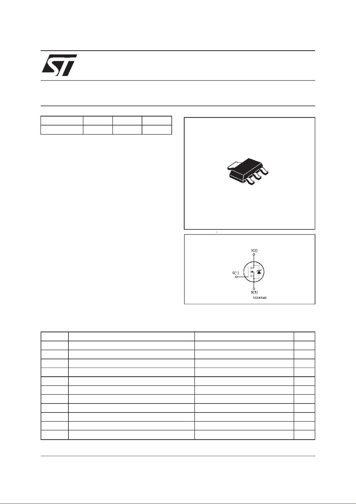
2
3
2
1
SOT-223
INTERNAL SCHEMATIC DIAGRAM
ABSOLUTE MAXIMUM RATINGS
Symbol Parameter Value Uni t
V
V
V
I
DM
P
dv/ dt (
T
(•) Pulse width limited by safe operating area (1)ISD≤ 8 A, di/dt ≤ 200 A/µs, VDD≤ V
April 1999
Drain-source Voltage (VGS=0) 60 V
DS
Drain- gate Volt age (RGS=20kΩ)60V
DGR
Gate-source Voltage ± 20 V
GS
I
Drain Current (continuous ) at Tc=25oC2A
D
I
Drain Current (continuous ) at Tc=100oC1.3A
D
(•) Drain Current (pulsed) 8 A
Total Dissipation at Tc=25oC2.5W
tot
Derat ing Factor 0.02 W/
1 ) Peak Diode Recovery voltage s lope 6 V/ns
Sto rage Temperature -65 t o 150
stg
T
Max. Operating Junct ion Temperat ur e 150
j
(BR)DSS,Tj≤TJMAX
o
C
o
C
o
C
1/8
Page 2
STN2NE06
THERMAL DATA
R
thj-pcb
R
thj-amb
T
AVALANCHE CHARACTERISTICS
Symbol Parameter Max Value Unit
I
AR
E
Ther mal Resistanc e Junct ion-PC Board Max
Ther mal Resistanc e Junct ion-ambient Max
(Surface Mounted)
Maximum Lead Te m perature For Soldering Purpos e
l
Avalanche Current, Repetitive or Not-Repetitive
(pulse width limited by T
Single Pulse Avalanche Energy
AS
(starting T
=25oC, ID=IAR,VDD=25V)
j
max)
j
50
60
260
2A
20 mJ
o
C/W
o
C/W
o
C
ELECTRICAL CHARACTERISTICS
=25oC unless otherwisespecified)
(T
case
OFF
Symbol Parameter Test Condit ions Min. Typ. Max. Unit
V
(BR)DSS
Drain-source
ID=250µAVGS=0 60 V
Break dow n Voltage
I
DSS
I
GSS
Zero Gate Voltage
Drain Current (V
GS
Gat e- bod y Leakage
Current (V
DS
=0)
=0)
V
=MaxRating
DS
=MaxRating Tc= 125oC
V
DS
V
=± 20 V
GS
1
10
100 nA
±
ON(∗)
Symbol Parameter Test Condit ions Min. Typ. Max. Unit
V
GS(th)
R
DS(on)
Gate Threshold Voltage VDS=VGSID= 250 µA 234V
Sta t ic Dr ain -s ource On
VGS=10V ID= 1 A 0.18 0.25
Resistance
I
D(on)
On State Drain Current VDS>I
D(on)xRDS(on )max
2A
VGS=10V
DYNAMIC
Symbol Parameter Test Condit ions Min. Typ. Max. Unit
g
(∗)Forward
fs
Tr ansc on duc tance
C
C
C
Input C apac i t ance
iss
Out put Capacitanc e
oss
Reverse T r ansfer
rss
Capacit a nc e
VDS>I
D(on)xRDS(on )maxID
=1A 1.8 S
VDS=25V f=1MHz VGS= 0 V 310
45
12.5
420
61
17
µ
µA
Ω
pF
pF
pF
A
2/8
Page 3
STN2NE06
ELECTRICAL CHARACTERISTICS
(continued)
SWITCHINGON
Symbol Parameter Test Condit ions Min. Typ. Max. Unit
t
d(on)
Q
Q
Q
Turn-on Time
Rise T i me
t
r
Tot al G at e Char ge
g
Gat e- Source Charge
gs
Gate-Drain Charge
gd
VDD=30V ID=1A
R
=4.7
G
Ω
VGS=10V
9
10
VDD=40V ID=2A VGS=10V 12
5.1
2.7
13
13.5
17
7
4
SWITCHINGOFF
Symbol Parameter Test Condit ions Min. Typ. Max. Unit
t
r(Voff)
t
t
Off-volt age R ise Time
Fall T ime
f
Cross-over T ime
c
VDD=48V ID=2A
=4.7ΩVGS=10V
R
G
4.5
5
12
6
7
16
SOURCEDRAINDIODE
Symbol Parameter Test Condit ions Min. Typ. Max. Unit
I
SD
I
SDM
V
SD
t
Q
I
RRM
(∗) Pulsed: Pulse duration = 300µs, duty cycle 1.5 %
(•) Pulse width limited by safe operating area
Source-drain Current
(•)
Source-drain Current
2
8
(pulsed)
(∗)ForwardOnVoltage ISD=2A VGS=0 1.2 V
Reverse Re covery
rr
Time
Reverse Re covery
rr
ISD= 2 A di/dt = 100 A/µs
=30V Tj=150oC
V
DD
40
50
Charge
Reverse Re covery
2.5
Current
ns
ns
nC
nC
nC
ns
ns
ns
A
A
ns
nC
Α
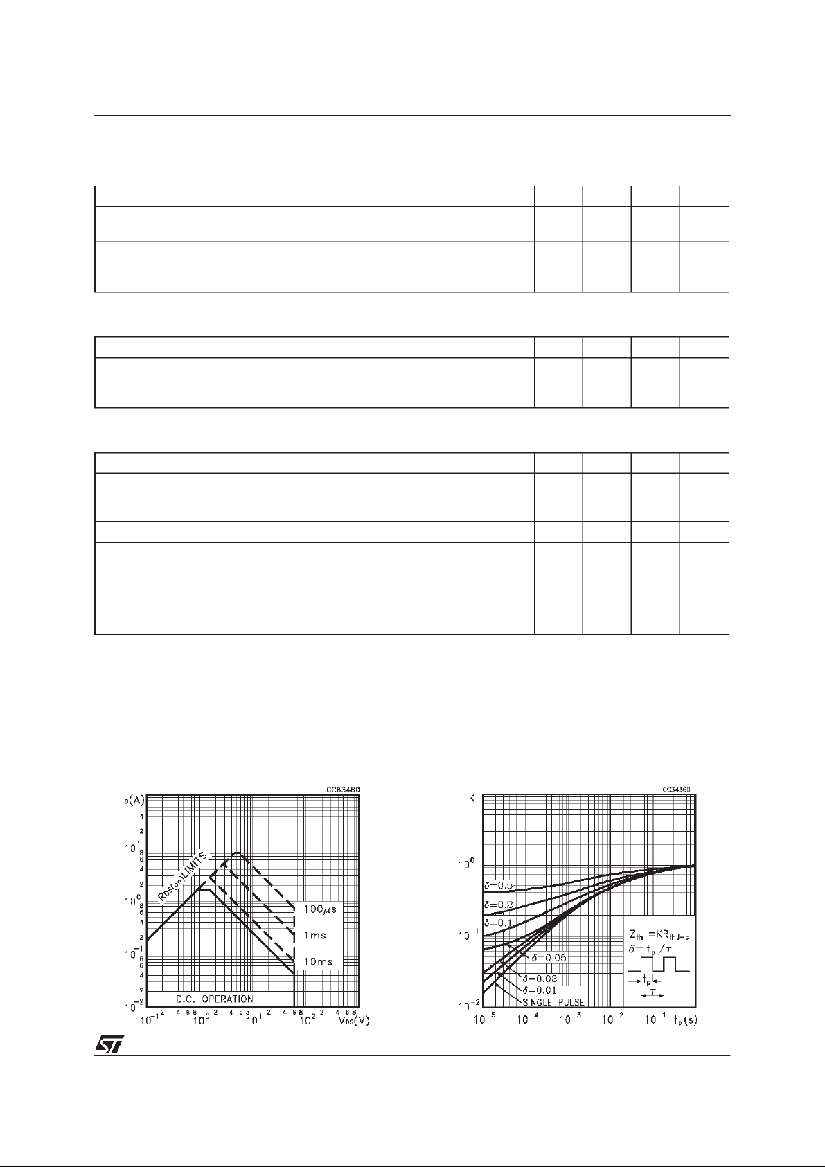
SafeOperating Area ThermalImpedance
3/8
Page 4

STN2NE06
OutputCharacteristics
Transconductance
TransferCharacteristics
Static Drain-sourceOn Resistance
Gate Charge vs Gate-sourceVoltage
4/8
CapacitanceVariations
Page 5

STN2NE06
NormalizedGate ThresholdVoltage vs
Temperature
Source-drainDiode Forward Characteristics
NormalizedOn Resistancevs Temperature
5/8
Page 6

STN2NE06
Fig. 1:
UnclampedInductiveLoad TestCircuit
Fig. 3: Switching Times Test CircuitsFor
ResistiveLoad
Fig. 2:
UnclampedInductiveWaveform
Fig. 4: Gate Charge test Circuit
Fig. 5:
Test CircuitFor InductiveLoad Switching
And Diode Recovery Times
6/8
Page 7

SOT-223 MECHANICALDATA
STN2NE06
DIM.
MIN. TYP. MAX. MIN. TYP. MAX.
a 2.27 2.3 2.33 89.4 90.6 91.7
b 4.57 4.6 4.63 179.9 181.1 182.3
c 0.2 0.4 0.6 7.9 15.7 23.6
d 0.63 0.65 0.67 24.8 25.6 26.4
e1 1.5 1.6 1.7 59.1 63 66.9
e4 0.32 12.6
f 2.9 3 3.1 114.2 118.1 122.1
g 0.67 0.7 0.73 26.4 27.6 28.7
l1 6.7 7 7.3 263.8 275.6 287.4
l2 3.5 3.5 3.7 137.8 137.8 145.7
L 6.3 6.5 6.7 248 255.9 263.8
mm mils
L
e1
a
b
f
C
l1
BE
C
g
d
l2
c
e4
P008B
7/8
Page 8

STN2NE06
Information furnishedis believedto beaccurate and reliable.However, STMicroelectronics assumes no responsibilityfor the consequences
of use of such information nor for any infringement of patents or other rights of third parties which may result from its use. No license is
granted by implication or otherwise under anypatent or patent rights ofSTMicroelectronics. Specificationmentioned in this publicationare
subjecttochange withoutnotice.This publication supersedes andreplaces all informationpreviously supplied.STMicroelectronics products
are not authorized for use as critical components in lifesupportdevices or systems without express written approval of STMicroelectronics.
The ST logo is a trademark of STMicroelectronics
1999 STMicroelectronics – Printed in Italy – All Rights Reserved
STMicroelectronics GROUP OF COMPANIES
Australia - Brazil - Canada - China - France - Germany - Italy - Japan - Korea - Malaysia - Malta - Mexico - Morocco - The Netherlands -
8/8
Singapore - Spain - Sweden - Switzerland - Taiwan - Thailand - United Kingdom - U.S.A.
http://www.st.com
.
 Loading...