

Page 1
N - CHANNEL ENHANCEMENT MODE
TYPE V
DSS
STN2N06 60 V < 0.250 Ω 2 A
R
DS(on)
I
D
CONT
STN2N06
POWER MOS TRANSISTOR
ADVANCE DATA
■ TYPICAL R
■ AVALANCHE RUGGED TECHNOLOGY
■ SOT-223 CAN BE WAVE OR REFLO W
DS(on)
= 0.21 Ω
SOLDERED
■ AVAILABLE IN TAPE AND REEL ON
REQUEST
o
■ 150
■ APPLICATION ORIENTED
C OPERATING TEMPERATURE
CHARACTERIZATION
APPLICATIONS
■ HARD DISK DRIVERS
■ SMALL MOTOR CURRENT SENS E
CIRCUITS
■ DC-DC CONVERTE RS A ND PO WER
SUPPLIES
2
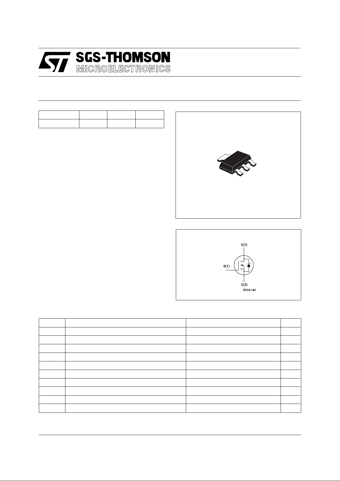
3
2
1
SOT-223
INTERNAL SCHEMATIC DIAGRAM
ABSOL UT E MAXIMU M RATINGS
Symbol Parameter Value Unit
V
V
V
I
D
I
D
I
DM
P
T
(•) Pulse width limited by safe operating area (*) Limited by package
March 1996
Drain-source Voltage (VGS = 0) 60 V
DS
Drain- gate Voltage (RGS = 20 kΩ)60V
DGR
Gate-source Voltage ± 20 V
GS
(*) Drain Current (continuous) at Tc = 25 oC2A
(*) Drain Current (continuous) at Tc = 100 oC 1.3 A
(•) Drain Current (pulsed) 8 A
Total Dissipation at Tc = 25 oC 2.7 W
tot
Derating Factor 0.022 W/
Storage Temperature -65 to 150
stg
T
Max. Operating Junction Temperature 150
j
o
C
o
C
o
C
1/5
Page 2
STN2N06
THERMAL DATA
R
thj-pcb
R
thj-amb
Thermal Resistance Junction-PC Board Max
Thermal Resistance Junction-ambient Max
(Surface Mounted)
T
Maximum Lead Temperature For Soldering Purpose
l
AVALANCHE CHARACTERI S TICS
Symbol Parameter Max Value Unit
I
AR
E
E
I
AR
Avalanche Current, Repetitive or Not-Repetitive
(pulse width limited by T
Single Pulse Avalanche Energy
AS
(starting T
Repetitive Avalanche Energy
AR
= 25 oC, ID = IAR, V
j
(pulse width limited by T
max, δ < 1%)
j
DD
max, δ < 1%)
j
Avalanche Current, Repetitive or Not-Repetitive
(T
= 100 oC, pulse width limited by Tj max, δ < 1%)
c
= 25 V)
46
60
260
2A
40 mJ
10 mJ
1.3 A
o
C/W
o
C/W
o
C
ELECTRICAL CHARACTERISTICS (T
= 25 oC unless otherwise specified)
case
OFF
Symbol Parameter Test Conditions Min. Typ. Max. Unit
V
(BR)DSS
Drain-source
ID = 250 µA V
= 0 60 V
GS
Breakdown Voltage
I
DSS
I
GSS
Zero Gate Voltage
Drain Current (V
GS
Gate-body Leakage
Current (V
DS
= 0)
= 0)
= Max Rating
V
DS
V
= Max Rating x 0.8 Tc = 125 oC
DS
= ± 20 V ± 100 nA
V
GS
250
1000µAµA
ON (∗)
Symbol Parameter Test Conditions Min. Typ. Max. Unit
V
GS(th)
R
DS(on)
I
D(on)
Gate Threshold Voltage V
Static Drain-source On
Resistance
= VGS ID = 250 µA 234V
DS
VGS = 10 V ID = 1 A
V
= 10 V ID = 1 A Tc = 100oC
GS
On State Drain Current VDS > I
V
= 10 V
GS
D(on)
x R
DS(on)max
0.21 0.25
0.5
2A
DYNAMIC
Symbol Parameter Test Conditions Min. Typ. Max. Unit
g
(∗) Forward
fs
Transconductance
C
C
C
Input Capacitance
iss
Output Capacitance
oss
Reverse Transfer
rss
Capacitance
VDS > I
V
DS
x R
D(on)
DS(on)max
= 25 V f = 1 MHz V
ID = 1 A 0.8 1.5 S
= 0 V 260
GS
90
30
340
120
40
Ω
Ω
pF
pF
pF
2/5
Page 3

STN2N06
ELECTRICAL CHARACTERISTICS (continued)
SWITCHING O N
Symbol Parameter Test Conditions Min. Typ. Max. Unit
t
d(on)
(di/dt)
Q
Q
Q
SWITCHING O F F
Symbol Parameter Test Conditions Min. Typ. Max. Unit
t
r(Voff)
t
SOURCE DRAIN DIO DE
Symbol Parameter Test Conditions Min. Typ. Max. Unit
I
SD
I
SDM
V
SD
t
Q
I
RRM
(∗) Pulsed: Pulse duration = 300 µs, duty cycle 1.5 %
(•) Pulse width limited by safe operating area
Turn-on Time
Rise Time
t
r
Turn-on Current Slope V
on
Total Gate Charge
g
Gate-Source Charge
gs
Gate-Drain Charge
gd
Off-voltage Rise Time
Fall Time
t
f
Cross-over Time
c
Source-drain Current
(•)
Source-drain Current
V
= 30 V ID = 4 A
DD
R
= 47 Ω VGS = 10 V
G
= 48 V ID = 8 A
DD
R
= 47 Ω VGS = 10 V
G
V
= 48 V ID = 8 A V
DD
V
= 48 V ID = 8 A
DD
R
= 47 Ω VGS = 10 V
G
= 10 V 13
GS
14
75
20
100
240 A/µs
20 nC
7
4
16
22
45
25
30
60
2
8
(pulsed)
(∗) Forward On Voltage ISD = 2 A VGS = 0 1.5 V
Reverse Recovery
rr
Time
Reverse Recovery
rr
I
= 8 A di/dt = 100 A/µs
SD
V
= 25 V Tj = 150 oC
DD
70
0.18
Charge
Reverse Recovery
5
Current
ns
ns
nC
nC
ns
ns
ns
A
A
ns
µC
A
3/5
Page 4

STN2N06
SOT223 MECHANICAL DATA
DIM.
MIN. TYP. MAX. MIN. TYP. MAX.
a 2.27 2.3 2.33 89.4 90.6 91.7
b 4.57 4.6 4.63 179.9 181.1 182.3
c 0.2 0.4 0.6 7.9 15.7 23.6
d 0.630.650.6724.825.626.4
e1 1.5 1.6 1.7 59.1 63 66.9
e4 0.32 12.6
f 2.9 3 3.1 114.2 118.1 122.1
g 0.67 0.7 0.73 26.4 27.6 28.7
l1 6.7 7 7.3 263.8 275.6 287.4
l2 3.5 3.5 3.7 137.8 137.8 145.7
L 6.3 6.5 6.7 248 255.9 263.8
mm mils
l1
e1
L
a
b
f
C
B
C
E
g
d
l2
c
e4
P008B
4/5
Page 5

STN2N06
Information furnished is believed to be accurate and reliable. However, SGS-THOMSON Microelectronics assumes no responsability for the
consequences of use of such information nor for any infringement of pat e nt s or other rights of third parties which may results from its use. No
license is granted by implication or otherwise under any patent or patent rights of SGS-TH OMSON Microelectronics. Specificati ons mentione d
in this publication are subject to cha nge wi t hout no t ice. This p u bli ca tion su p e rsed e s and r epla ces al l infor mat i on pr ev io us ly supplied.
SGS-THOMSON Microelectronics products are not authorize d for use as critical components in life support devices or systems without express
written approval of SGS-THOMSO N M icroele cton ics.
© 1995 SGS-THOMSON Microelectronics - All Rights Reserved
Australia - Brazil - France - Germany - Hong Ko ng - Ita ly - Japa n - Korea - Mal ay sia - Mal ta - Mor oc co - The Net her l ands -
Singapore - Spain - Sweden - Switzerland - Taiwan - Thailand - United Kingdom - U.S.A
SGS-THOMSON Microelectronics GROUP OF COMPANIES
. . .
5/5
 Loading...