

Page 1
STN1N20
N - CHANNEL 200V - 1.2
TYPE V
DSS
ST N1N2 0 200 V < 1.5 Ω 1A
■ TYPICALR
■ AVALANCHERUGGEDTECHNOLOGY
■ SOT-223CAN BE WAVEOR REFLOW
DS(on)
= 1.2 Ω
SOLDERED
■ AVAILABLEIN TAPEAND REELON
REQUEST
o
■ 150
■ APPLICATIONORIENTED
C OPERATINGTEMPERATURE
CHARACTERIZATION
APPLICATIONS
■ HARDDISK DRIVERS
■ SMALLMOTORCURRENT SENSE
CIRCUITS
■ DC-DCCONVERTERS AND POWER
SUPPLIES
R
DS(on)
I
CONT
D
Ω
- 1A - SOT-223
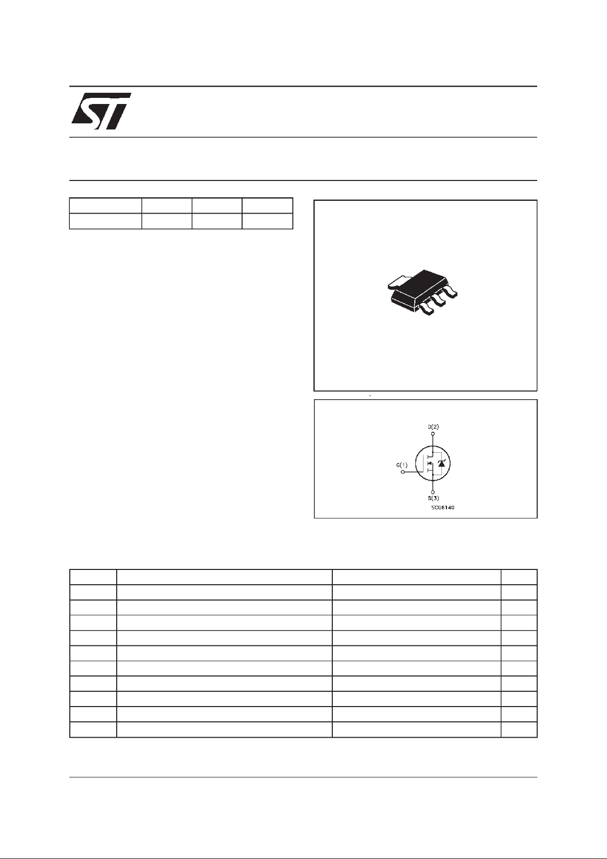
POWER MOS TRANSISTOR
PRELIMINARY DATA
2
3
2
1
SOT-223
INTERNAL SCHEMATIC DIAGRAM
ABSOLUTE MAXIMUM RATINGS
Symb o l Parameter Value Unit
V
V
V
I
D
I
D
I
DM
P
T
(•) Pulse width limited by safeoperating area (*) Limited by package
September 1999
Drain-source Voltage (VGS= 0) 200 V
DS
Drain- gate Volt ag e (RGS=20kΩ) 200 V
DGR
Gate-s ource Voltage
GS
20 V
±
(*) Drain Current (co ntinuous) at Tc=25oC1A
(*) Drain Current (co ntinuous) at Tc=100oC 0.6 A
(•) Drain Curr ent (pu lsed) 4 A
Tot al Di ss i pat ion at Tc=25oC 2.9 W
tot
Derat ing Factor 0.023 W/
Sto rage Tem per at ur e -65 t o 15 0
stg
T
Max. Operat ing Junct ion T emperat ure 150
j
o
C
o
C
o
C
1/6
Page 2
STN1N20
THERMAL DATA
R
thj-pcb
R
thj-amb
T
AVALANCHE CHARACTERISTICS
Symbol Parameter Max V alue Unit
I
AR
E
Ther mal Resistanc e Junct ion-PC B oa rd Max
Ther mal Resistanc e Junct ion-ambient Max
(Surface Mounted)
Maximum Lead Te m perature For Soldering Purpos e
l
Avalanche C urrent, R epetitive or Not-Repetitive
(pulse width limited by T
Single P ul s e Avalan c he Energy
AS
(starting T
=25oC, ID=IAR,VDD=25V)
j
max)
j
43
60
260
1A
10 mJ
o
C/W
o
C/W
o
C
ELECTRICAL CHARACTERISTICS
=25oC unless otherwisespecified)
(T
case
OFF
Symbol Parameter Test Conditions Min. Typ. M ax. Unit
V
(BR)DSS
Drain-source
ID=250µAVGS= 0 200 V
Break dow n Voltage
I
DSS
I
GSS
Zero Gate Voltage
Drain Current (V
GS
Gat e- bod y L eak ag e
Current (V
DS
=0)
=0)
V
=MaxRating
DS
=MaxRating Tc= 125oC
V
DS
V
=± 20 V
GS
10
100
100 nA
±
ON(∗)
Symbol Parameter Test Conditions Min. Typ. M ax. Unit
V
GS(th)
R
DS(on)
Gate Threshold Voltage VDS=VGSID= 250 µ A 234V
Sta t ic Drain -s ource On
VGS=10V ID= 0.5 A 1.2 1.5
Resistance
I
D(on)
On State Drain Current VDS>I
D(on)xRDS(on )max
1A
VGS=10V
DYNAMIC
Symbol Parameter Test Conditions Min. Typ. M ax. Unit
g
(∗)Forward
fs
Tr ansc on duc tance
C
C
C
Input Capac i t anc e
iss
Out put Capacitanc e
oss
Reverse Tr ansfer
rss
Capacit a nc e
VDS>I
D(on)xRDS(on )maxID
=0.5A 0.3 0.7 S
VDS=25V f=1MHz VGS= 0 V 290
50
10
400
70
15
µ
µA
Ω
pF
pF
pF
A
2/6
Page 3

STN1N20
ELECTRICAL CHARACTERISTICS
(continued)
SWITCHINGON
Symbol Parameter Test Conditions Min. Typ. M ax. Unit
t
d(on)
(di/dt)
Q
Q
Q
Turn-on Time
Rise Ti m e
t
r
Tur n-on Current S lop e VDD=160V ID=4A
on
Tot al Gat e Charge
g
Gat e- Source Charg e
gs
Gate-Drain Charge
gd
VDD=100V ID=2A
R
=4.7
Ω
G
=47
R
Ω
G
VDD= 160 V ID=4A VGS=10V 13
VGS=10V
VGS=10V
7
6
10
10
270 A/ µs
20 nC
7
4
SWITCHINGOFF
Symbol Parameter Test Conditions Min. Typ. M ax. Unit
t
r(Voff)
t
Off-volt age Rise Time
Fall T ime
t
f
Cross-over T im e
c
VDD=160V ID=4A
R
=4.7 ΩVGS=10V
G
13
6
5
10
10
20
SOURCEDRAINDIODE
Symbol Parameter Test Conditions Min. Typ. M ax. Unit
I
SD
I
SDM
V
SD
t
Q
I
RRM
(∗) Pulsed:Pulse duration = 300µs, duty cycle 1.5%
(•) Pulse width limited by safe operating area
Source-drain Current
(•)
Source-drain Current
1
4
(pulsed)
(∗)ForwardOnVoltage ISD=1A VGS=0 1.5 V
Reverse Recover y
rr
Time
Reverse Recover y
rr
ISD= 4 A di/dt = 100 A/µs
=30V Tj= 150oC
V
DD
170
1
Charge
Reverse Recover y
12
Current
ns
ns
nC
nC
ns
ns
ns
A
A
ns
µ
A
C
3/6
Page 4

STN1N20
Fig. 1:
UnclampedInductiveLoad TestCircuit
Fig. 3: SwitchingTimes Test Circuits For
ResistiveLoad
Fig. 2:
UnclampedInductiveWaveform
Fig. 4: Gate Chargetest Circuit
Fig. 5:
Test CircuitFor InductiveLoad Switching
And Diode Recovery Times
4/6
Page 5

SOT-223 MECHANICALDATA
STN1N20
DIM.
MIN. TYP. MAX. MIN. TYP. MAX.
a 2.27 2.3 2.33 89.4 90.6 91.7
b 4.57 4.6 4.63 179.9 181.1 182.3
c 0.2 0.4 0.6 7.9 15.7 23.6
d 0.63 0.65 0.67 24.8 25.6 26.4
e1 1.5 1.6 1.7 59.1 63 66.9
e4 0.32 12.6
f 2.9 3 3.1 114.2 118.1 122.1
g 0.67 0.7 0.73 26.4 27.6 28.7
l1 6.7 7 7.3 263.8 275.6 287.4
l2 3.5 3.5 3.7 137.8 137.8 145.7
L 6.3 6.5 6.7 248 255.9 263.8
mm mils
L
e1
a
b
f
C
l1
BE
C
g
d
l2
c
e4
P008B
5/6
Page 6

STN1N20
Information furnishedis believed to beaccurate and reliable.However, STMicroelectronics assumes no responsibilityforthe consequences
of use of such information nor for any infringement of patents or other rights of third parties which may result from its use. No license is
granted by implication or otherwise under anypatent or patent rights ofSTMicroelectronics. Specificationmentioned in this publication are
subjecttochange withoutnotice.This publication supersedes andreplaces all informationpreviously supplied.STMicroelectronics products
are not authorized for use as critical components in lifesupportdevices or systems without express written approval of STMicroelectronics.
The STlogo is a trademark of STMicroelectronics
1999 STMicroelectronics – Printed in Italy – All Rights Reserved
STMicroelectronics GROUP OF COMPANIES
Australia - Brazil - China - Finland - France - Germany - Hong Kong - India - Italy- Japan - Malaysia - Malta - Morocco -
6/6
Singapore - Spain - Sweden - Switzerland - United Kingdom - U.S.A.
http://www.st.com
.
 Loading...