

Page 1
Features
STMUX1800L
16- to 8-bit MUX/DEMUX for gigabit Ethernet LAN switch
with LED switch and enhanced ESD protection
■ Low R
■ V
CC
■ Enhanced ESD protection: > 8 kV (contact) and
: 4.0 Ω typical
ON
operating range: 3.0 to 3.6 V
15 kV (HBM)
■ Channel on capacitance: 9.5 pF typical
■ Switching time speed: 9 ns
■ Near to zero propagation delay: 250 ps
■ Very low crosstalk: -45 dB at 250 MHz
■ Bit-to-bit skew: 200 ps
■ > 600 MHz -3 dB typical bandwidth (or data
frequency)
■ Three SPDT switches for LED support
■ Rail-to-rail switching on data I/O ports
(0 V to 5 V)
■ Package: QFN56
■ Pb-free
Applications
■ 10/100/1000 Mbit Ethernet switching
■ Audio/video switching
QFN56
Description
The STMUX1800L is a 16- to 8-bit
multiplexer/demultiplexer low R
LAN switch designed for various standards, such
as 10/100/1000 Ethernet. It is designed for very
low crosstalk, low bit-to-bit skew and low I/O
capacitance.
bidirectional
ON
The differential signal from the Gigabit Ethernet
transceiver is multiplexed into one of two selected
outputs while the unselected switch goes to Hi-Z
status.
The device integrates three SPDT (single pole
dual throw) switches, for LED support.
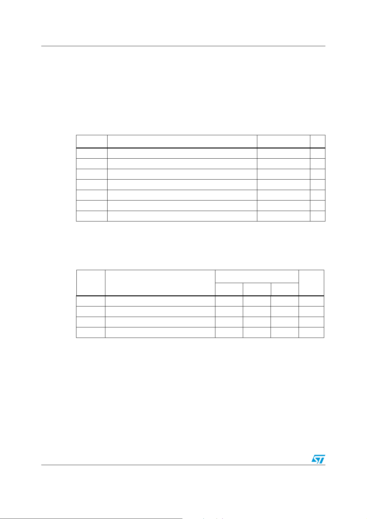
Table 1. Device summary
Order code Package Packing
STMUX1800LQTR QFN56 Tape and reel
June 2009 Doc ID 14869 Rev 4 1/21
www.st.com
21
Page 2

Contents STMUX1800L
Contents
1 Pin description . . . . . . . . . . . . . . . . . . . . . . . . . . . . . . . . . . . . . . . . . . . . . 3
2 Maximum ratings . . . . . . . . . . . . . . . . . . . . . . . . . . . . . . . . . . . . . . . . . . . . 6
2.1 Recommended operating conditions . . . . . . . . . . . . . . . . . . . . . . . . . . . . . 6
3 Electrical characteristics . . . . . . . . . . . . . . . . . . . . . . . . . . . . . . . . . . . . . 7
4 Package mechanical data . . . . . . . . . . . . . . . . . . . . . . . . . . . . . . . . . . . . 16
5 Revision history . . . . . . . . . . . . . . . . . . . . . . . . . . . . . . . . . . . . . . . . . . . 20
2/21 Doc ID 14869 Rev 4
Page 3
STMUX1800L Pin description
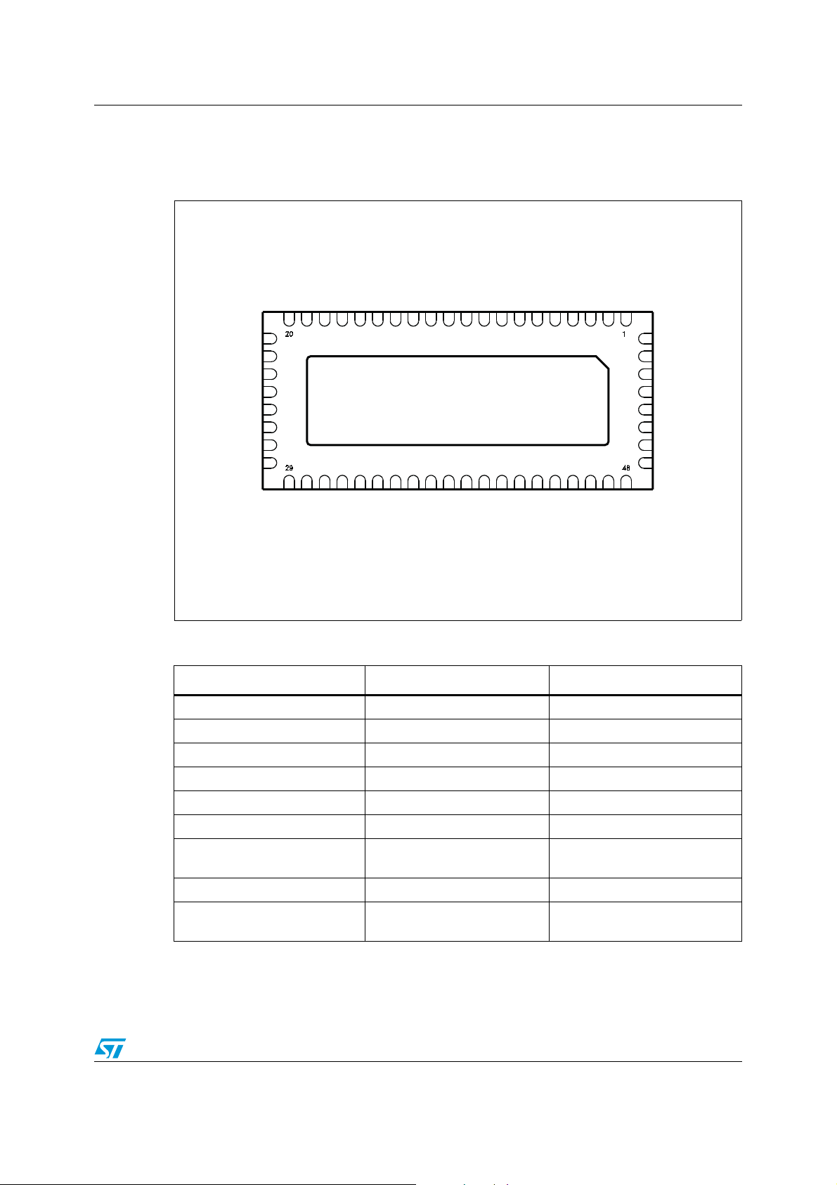
1 Pin description
Figure 1. Pin connection (top through view)
LED2
LED1
VDD
SEL
GNDHG
GNDFE
VDD
GNDDC
GND
N/C
VDDBA
GND
GND
LED1_0
LED2_0
GND
LED1_1
LED2_1
VDD
GND
F1
F0
H1G1H0
G0
GND
E1
E0
VDD
D1C1D0
GND
C0
GND
B1A1B0
A0
Table 2. Pin description
Pin Symbol Name and function
2, 3, 7, 8, 11, 12, 14, 15 A, B, C, D, E, F, G, H 8-bit bus
48, 47, 43, 42, 37, 36, 32, 31 A0, B0, C0, D0, E0, F0, G0, H0 8-bit multiplexed to bus 0
46, 45, 41, 40, 35, 34, 30, 29 A1, B1, C1, D1, E1, F1, G1, H1 8-bit multiplexed to bus 1
VDD
GND
LED3
GND
LED3_0
LED3_1
VDD
GND
CS000103
5 N/C Not connected
17 SEL Bus and LED switch selection
19, 20, 54 LED1, LED2, LED3 LED switch input
22, 23, 25, 26, 51, 52
4, 10, 18, 27, 38, 50, 56 V
1, 6, 9, 13, 16, 21, 24, 28, 33,
39, 44, 49, 53, 55
LED1_0, LED2_0, LED1_1,
LED2_1, LED3_1, LED3_0
DD
GND Ground
LED switch output
Supply voltage
Doc ID 14869 Rev 4 3/21
Page 4
Pin description STMUX1800L
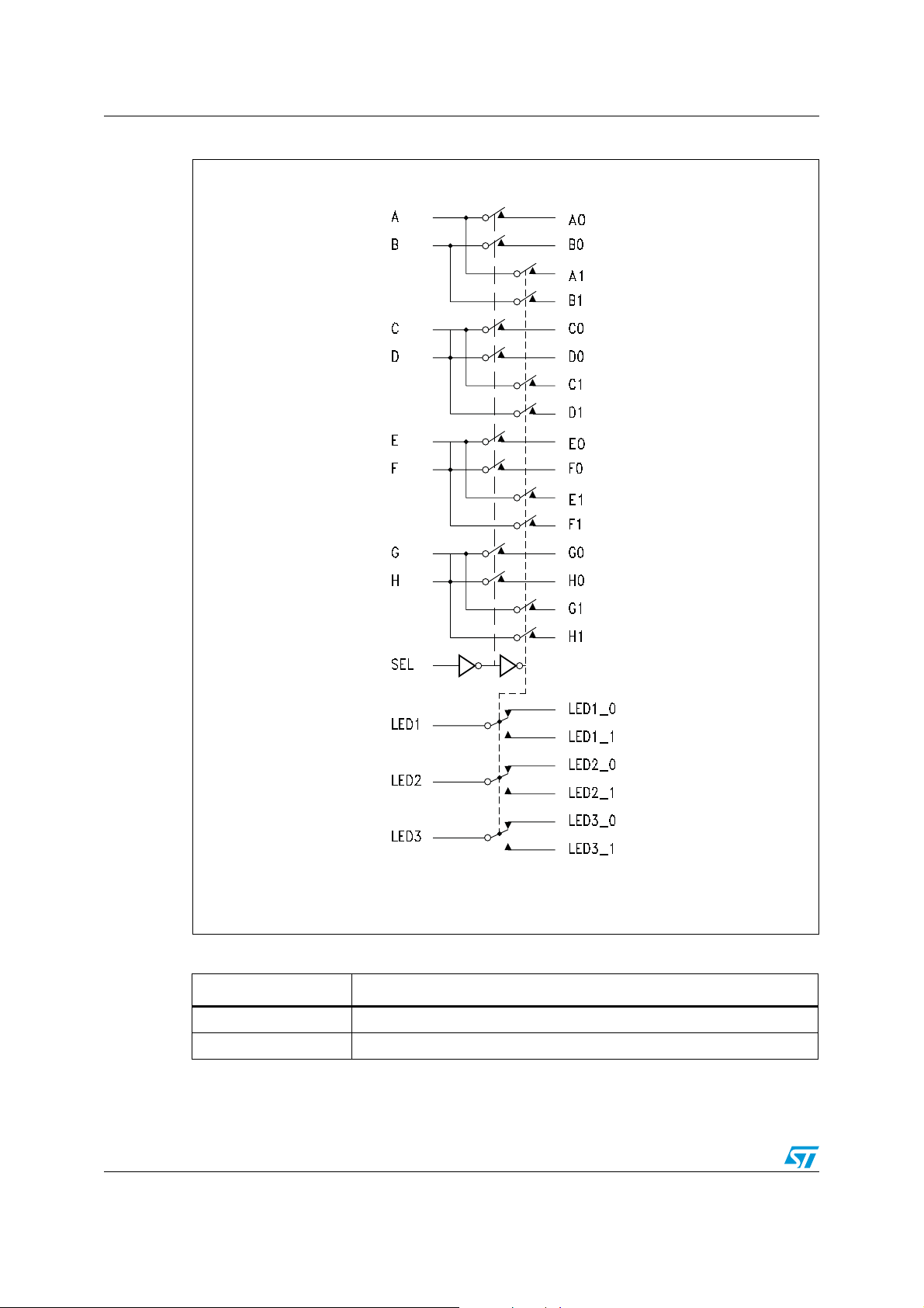
Figure 2. Input equivalent circuit
Table 3. LAN switch function table
SEL Function
L 8-bit bus to 8-bit multiplexed bus 0
H 8-bit bus to 8-bit multiplexed bus 1
4/21 Doc ID 14869 Rev 4
CS000104
Page 5
STMUX1800L Pin description
Table 4. LED switch function table
SEL Function
L LED switch input connected to LED switch output X_0
H LED switch input connected to LED switch output X_1
Doc ID 14869 Rev 4 5/21
Page 6
Maximum ratings STMUX1800L
2 Maximum ratings
Stressing the device above the rating listed in the “absolute maximum ratings” table may
cause permanent damage to the device. These are stress ratings only and operation of the
device at these or any other conditions above those indicated in the operating sections of
this specification is not implied. Exposure to absolute maximum rating conditions for
extended periods may affect device reliability.
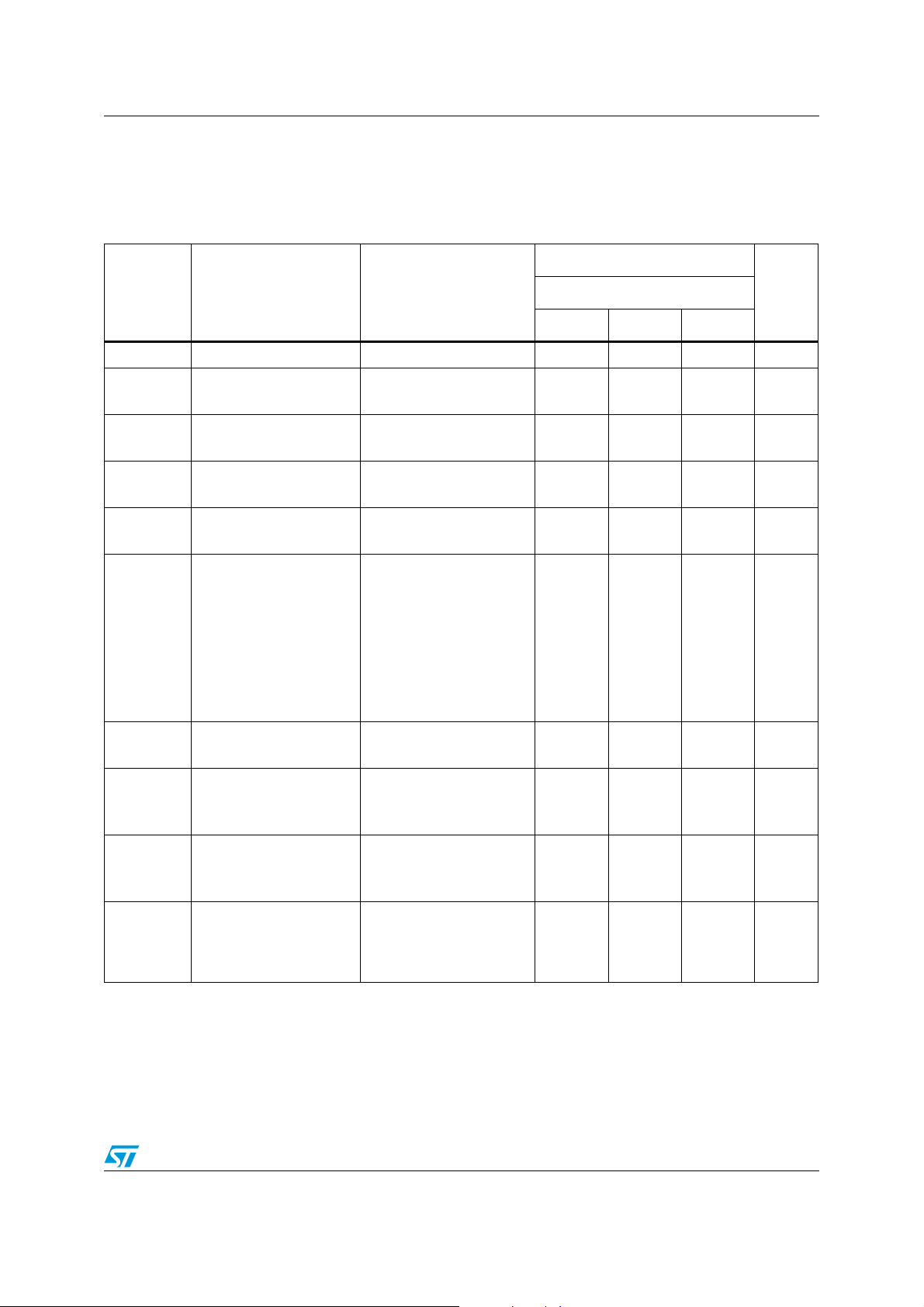
Table 5. Absolute maximum ratings
Symbol Parameter Value Unit
V
CC
V
V
I
O
P
T
stg
T
Supply voltage to ground -0.5 to 4.6 V
DC input output voltage -0.5 to 4.6 V
IO
DC control input voltage -0.5 to 4.6 V
IC
DC output current
Power dissipation 0.5 W
D
(1)
Storage temperature -65 to 150 °C
Lead temperature (10 sec) 300 °C
L
1. If VIO x IO does not exceed the maximum limit of PD.
2.1 Recommended operating conditions
Table 6. Recommended operating conditions
Symbol Parameter
V
V
V
T
Supply voltage to ground 3 – 3.6 V
CC
DC control input voltage (SEL) 0 – 5 V
IC
DC input/output voltage 0 – V
IO
Operating temperature -40 – 85 ° C
A
120 mA
Val ue
Min Typ Max
CC
Unit
V
6/21 Doc ID 14869 Rev 4
Page 7
STMUX1800L Electrical characteristics
3 Electrical characteristics
Table 7. DC electrical characteristics for Gigabit Ethernet LAN8/16MUX/DEMUX
(V
= 3.3 V ±10%)
CC
Val ue
Symbol Parameter Test condition
Min Typ Max
IOFF
V
V
V
I
I
IH
IL
IK
IH
IL
(SW)
Voltage input high (SEL) High level guaranteed 2 – – V
Voltage input low
(SEL)
Clamp diode voltage
(SEL)
Input high current
(SEL)
Input low current
(SEL)
Leakage current through
the switch common
(1)
terminals (A to H)
(LED1 to LED3)
Low level guaranteed -0.5 – 0.8 V
VCC = 3.6 V
IIN = -18 mA
VCC = 3.6 V
= V
V
IN
CC
VCC = 3.6 V
= GND
V
IN
= 3.6 V
V
CC
A to H = V
CC
LED1 to LED3 = V
A0 to H0 = 0 V
A1 to H1 = floating
CC
– -0.8 -1.2 V
––±5µA
––±5µA
––±1µA
LEDx_0 = 0 V
LEDx1 = floating
IOFF
(SEL)
SEL pin leakage current
SEL = V
VCC= 0 V
SEL = 0 to 3.6 V
CC
––±1µA
VCC = 3.0 V
R
ON
Switch ON resistance
(2)
= 1.5 to V
V
IN
CC
–4.06.5Ω
IIN = -40 mA
Unit-40 to 85 °C
VCC = 3.0 V
R
FLAT
ON resistance flatness
(3)
ON resistance match
ΔR
1. Refer to Figure 4: Test circuit for leakage current (IOFF) on page 11
2. Measured by voltage drop between channels at indicated current through the switch. ON resistance is determined by the
lower of the voltages.
3. Flatness is defined as the difference between the R
ΔR
4.
ON
between channel
ON
ΔR
= R
ON
(2)(4)
measured at same VCC, temperature and voltage level.
ONMAX-RONMIN
(2)
V
IN
I
IN
VCC = 3.0 V
V
IN
IIN = -40 mA
at 1.5 and VCC
= -40 mA
= 1.5 to V
ONMAX
CC
and R
–0.5–Ω
–0.41Ω
of ON resistance over the specified range.
ONMIN
Doc ID 14869 Rev 4 7/21
Page 8

Electrical characteristics STMUX1800L
Table 8. DC electrical characteristics for 10/100 Ethernet LAN8/16MUX/DEMUX
(V
= 3.3 V ±10)
CC
Val ue
Symbol Parameter Test condition
Min Typ Max
Voltage input high
(SEL)
Voltage input low
IL
(SEL)
Clamp diode voltage
IK
(SEL)
Input high current
(SEL)
Input low current
(SEL)
Leakage current
through the switch
(1)
common terminals (A to
H)
(LED1 to LED3)
High level guaranteed 2 – – V
Low level guaranteed -0.5 – 0.8 V
VCC = 3.6 V
IIN = -18 mA
VCC = 3.6 V
VIN = V
CC
VCC = 3.6 V
= GND
V
IN
= 3.6 V
V
CC
A to H = V
CC
LED1 to LED3 = V
A0 to H0 = 0 V
A1 to H1 = floating
CC
– -0.7 -1.2 V
––±5µA
––±5µA
––±1µA
LEDx_0 = 0 V
IOFF
V
IH
V
V
I
IH
I
IL
(SW)
LEDx1 = floating
IOFF
SEL pin leakage current
(SEL)
SEL = V
VCC= 0 V
SEL = 0 to 3.6 V
CC
––±1µA
VCC = 3.0 V
R
ON
Switch ON resistance
(2)
= 1.5 to V
V
IN
CC
–4.06.5Ω
IIN = -10 to -30 mA
Unit-40 to 85 °C
R
FLAT
ON resistance flatness
(2) (3)
ON resistance match
ΔR
1. Refer to Figure 4: Test circuit for leakage current (IOFF) on page 11
2. Measured by voltage drop between channels at indicated current through the switch. ON resistance is determinate by the
lower of the two voltages.
3. Flatness is defined as the difference between the R
ΔR
4.
between channel
ON
ΔR
= R
ON
ONMIN
(2)(4)
R
measured at same VCC, temperature and voltage level.
ON
ONMAX
-
VCC = 3.0 V
VIN at 1.5 and V
I
= -10 to -30 mA
IN
CC
VCC = 3.0 V
= 1.5 to V
V
IN
CC
IIN = -10 to -30 mA
and R
ONMAX
–0.5–Ω
–0.41Ω
of ON resistance over the specified range.
ONMIN
8/21 Doc ID 14869 Rev 4
Page 9

STMUX1800L Electrical characteristics
Table 9. Capacitance (TA = 25 °C, f = 1 MHz)
Val ue
Symbol Parameter Test condition
Min Typ Max
Unit
DC = 0.25 V
AC = 0.5 V
f=1MHz
DC = 0.25 V
AC = 0.5 V
f=1MHz
DC = 0.25 V
AC = 0.5 V
f=1MHz
PP
PP
PP
IN
OFF
ON
SEL pin input
capacitance
Switch off
capacitance
Switch on
capacitance
(1)
(2)
(3)
C
C
C
1. Refer to Figure 5 on page 12
2. Refer to Figure 6 on page 12
3. Refer to Figure 7 on page 13
Table 10. Power supply characteristics
Symbol Parameter Test condition
I
Quiescent power
CC
supply
VCC = 3.6 V, VIN = VCC or
GND
–23pF
–45pF
– 9.5 11 pF
Val ue
Unit-40 to 85 °C
Min Typ Max
– 150 500
µA
Table 11. Dynamic electrical characteristics (V
= 3.3 V ±10%)
CC
Val ue
Symbol Parameter Test condition
Unit-40 to 85 °C
Min Typ Max
(3)
RL= 100 Ω
f = 250 MHz
RL= 100 Ω
f = 250 MHz
RL= 100 Ω
< V
≤ 3.6 V
0
IN
–-45–dB
–-37–dB
– 600 – MHz
X
O
talk
IRR
Crosstalk
Off isolation
(1)
(2)
BW -3 dB bandwidth
1. Refer to Figure 9 on page 14
2. Refer to Figure 10 on page 15
3. Refer to Figure 8 on page 13
Doc ID 14869 Rev 4 9/21
Page 10

Electrical characteristics STMUX1800L
Table 12. Switching characteristics (TA = 25 °C, VCC = 3.3 V ±10%)
Val ue
Symbol Parameter Test condition
Min Typ Max
Unit
t
t
PZH
t
PZL
t
PHZ
t
PLZ
Propagation delay VCC = 3 to 3.6 V – 0.25 – ns
PD
,
Line enable time, SE
to x to x0 or x to x1
,
Line disable time, SE
to x to x0 or x to x1
V
CC
V
CC
Output skew
t
SK(O)
between center port
VCC = 3 to 3.6 V – 0.1 0.2 ns
to any other port
Skew between
t
SK(P)
opposite transition of
the same output
, t
PLH
)
(t
PHL
V
CC
Table 13. ESD performance
Symbol Test condition
Contact discharge
IEC61000-4-2
ESD
Human body model
(MIL-STD-883)
(1)
= 3 to 3.6 V 0.5 6.5 15 ns
= 3 to 3.6 V 0.5 6.5 8.5 ns
= 3 to 3.6 V – 0.1 0.2 ns
Val ue
Unit
Min Typ Max
–±8–kV
–±15–kV
1. Refer to Figure 3: Diagram for suggested VDD decoupling on page 11.
10/21 Doc ID 14869 Rev 4
Page 11

STMUX1800L Electrical characteristics
Figure 3. Diagram for suggested VDD decoupling
C=2uF or
4.7uF
Note: 100nF Capacitors must be used as local bypass capacitors between the adjacent VDD and GND pairs (total 7)
1. Applicable for system level ESD test
VDD
GND
1
VDD
4
GND
6
GND
9
VDD
10
GND
13
GND
16
VDD
18
21 24 27 28
GND
GND
GND
DUT
GND
VDD
GND
4950535556
GND
44
GND
39
VDD
38
GND
33
VDD
GND
Figure 4. Test circuit for leakage current (I
OFF
)
3.6 V
VDD
I
A0
OFF(SW)
A
FLOAT
A1
3.6 V
3.6 V
SEL
GND
Doc ID 14869 Rev 4 11/21
Page 12

Electrical characteristics STMUX1800L
Figure 5. Test circuit for SEL pin input capacitance (CIN)
3.3 V
VDD
LCR meter
DC = 0.25 V
AC = 0.5 Vpp
f = 1 MHz
SEL
DUT
GND
Figure 6. Test circuit for switch off capacitance (C
L or H
H for channel 0
and L for channel 1
SEL
LCR meter
DC = 0.25 V
AC = 0.5 Vpp
f = 1 MHz
A
OFF
DUT
)
3.3 V
VDD
A0
A1
GND
12/21 Doc ID 14869 Rev 4
Page 13

STMUX1800L Electrical characteristics
Figure 7. Test circuit for switch on capacitance (CON)
VDD
DUT
GND
3.3 V
A0
A1
LCR meter
DC = 0.25 V
AC = 0.5 Vpp
f = 1 MHz
L or H
L for channel 0 and
H for channel 1
SEL
A
Figure 8. Test circuit for bandwidth measurement (BW)
AA0
Frequency response is measured at the output of the ON channel. For example, when
= 0 and A is the input, the output is measured at A0. All unused analog I/O ports are
V
SEL
left open.
HP8753ES setup:
Average = 4
R
= 3 kHz
V
BW
BIAS
= 0.35 V
ST = 2 s
P1 = 0 dBm
Doc ID 14869 Rev 4 13/21
Page 14

Electrical characteristics STMUX1800L
Figure 9. Test circuit for crosstalk measurement (x
DUT
A0
B0
A1
B1
C0
D0
C1
D1
A
B
C
D
talk
)
Crosstalk is measured at the output of the non-adjacent ON channel. For example, when
= 0, and B is the input, the output is measured at D. All unused analog input ports are
V
SEL
connected to GND and output ports are left open.
HP8753ES setup:
Average = 4
R
= 3 kHz
BW
V
= 0.35 V
BIAS
ST = 2 s
P1 = 0 dBm
14/21 Doc ID 14869 Rev 4
Page 15

STMUX1800L Electrical characteristics
Figure 10. Test circuit for off isolation measurement (O
A
B
A0
B0
A1
B1
Off isolation is measured at the output of the OFF channel. For example, when V
IRR
)
=0, and
SEL
B is the input, the output is measured at B1. All unused analog input ports are connected to
GND and output ports are left open.
HP8753ES setup:
Average = 4
R
= 3 kHz
BW
V
= 0.35 V
BIAS
ST = 2 s
P1 = 0 dBm
Doc ID 14869 Rev 4 15/21
Page 16

Package mechanical data STMUX1800L
4 Package mechanical data
In order to meet environmental requirements, ST offers these devices in different grades of
ECOPACK
specifications, grade definitions and product status are available at: www.st.com.
ECOPACK
®
packages, depending on their level of environmental compliance. ECOPACK®
®
is an ST trademark.
Figure 11. Package outline for QFN56 (11 x 5 mm) pitch 0.5 mm
16/21 Doc ID 14869 Rev 4
7576329-A
Page 17

STMUX1800L Package mechanical data
Figure 12. Mechanical data for QFN56 (11 x 5 mm) pitch 0.5 mm
Millimeters
Symbol
Min Typ Max
A 0.700.750.80
A1 – – 0.05
A3 0.20 –
b 0.200.250.30
D 10.90 11.00 11.10
D2 8.30 8.40 8.50
D3 –9.50–
E 4.905.005.10
E2 2.30 2.40 2.50
E3 –3.50–
e – 0.50 –
L 0.300.400.50
Figure 13. Footprint recommendation for QFN56 (11 x 5 mm) pitch 0.5 mm
Doc ID 14869 Rev 4 17/21
Page 18

Package mechanical data STMUX1800L
Figure 14. Carrier tape information for QFN56 (11 x 5 mm) pitch 0.5 mm
7875978_K
18/21 Doc ID 14869 Rev 4
Page 19

STMUX1800L Package mechanical data
Figure 15. Reel information for QFN56 (11 x 5 mm) pitch 0.5 mm
Doc ID 14869 Rev 4 19/21
Page 20

Revision history STMUX1800L
5 Revision history
Table 14. Document revision history
Date Revision Changes
26-Feb-2008 1 Initial release.
Modified: datasheet title, channel on capacitance value from 7.5 pF
to 9.5 pF typical, Figure 1, Ta bl e 2 , Section 3: Electrical
24-Sep-2008 2
characteristics.
Added: fields of applications, Ta bl e 6 and QFN56 footprint
recommendations in Figure 13 on page 17.
30-Mar-2009 3
Updated: Features section, Table 5 on page 6, Table 11 on page 9
and Table 13 on page 10 and Chapter 4: Package mechanical data.
22-Jun-2009 4 Document promoted from Preliminary data to datasheet.
20/21 Doc ID 14869 Rev 4
Page 21

STMUX1800L
Please Read Carefully:
Information in this document is provided solely in connection with ST products. STMicroelectronics NV and its subsidiaries (“ST”) reserve the
right to make changes, corrections, modifications or improvements, to this document, and the products and services described herein at any
time, without notice.
All ST products are sold pursuant to ST’s terms and conditions of sale.
Purchasers are solely responsible for the choice, selection and use of the ST products and services described herein, and ST assumes no
liability whatsoever relating to the choice, selection or use of the ST products and services described herein.
No license, express or implied, by estoppel or otherwise, to any intellectual property rights is granted under this document. If any part of this
document refers to any third party products or services it shall not be deemed a license grant by ST for the use of such third party products
or services, or any intellectual property contained therein or considered as a warranty covering the use in any manner whatsoever of such
third party products or services or any intellectual property contained therein.
UNLESS OTHERWISE SET FORTH IN ST’S TERMS AND CONDITIONS OF SALE ST DISCLAIMS ANY EXPRESS OR IMPLIED
WARRANTY WITH RESPECT TO THE USE AND/OR SALE OF ST PRODUCTS INCLUDING WITHOUT LIMITATION IMPLIED
WARRANTIES OF MERCHANTABILITY, FITNESS FOR A PARTICULAR PURPOSE (AND THEIR EQUIVALENTS UNDER THE LAWS
OF ANY JURISDICTION), OR INFRINGEMENT OF ANY PATENT, COPYRIGHT OR OTHER INTELLECTUAL PROPERTY RIGHT.
UNLESS EXPRESSLY APPROVED IN WRITING BY AN AUTHORIZED ST REPRESENTATIVE, ST PRODUCTS ARE NOT
RECOMMENDED, AUTHORIZED OR WARRANTED FOR USE IN MILITARY, AIR CRAFT, SPACE, LIFE SAVING, OR LIFE SUSTAINING
APPLICATIONS, NOR IN PRODUCTS OR SYSTEMS WHERE FAILURE OR MALFUNCTION MAY RESULT IN PERSONAL INJURY,
DEATH, OR SEVERE PROPERTY OR ENVIRONMENTAL DAMAGE. ST PRODUCTS WHICH ARE NOT SPECIFIED AS "AUTOMOTIVE
GRADE" MAY ONLY BE USED IN AUTOMOTIVE APPLICATIONS AT USER’S OWN RISK.
Resale of ST products with provisions different from the statements and/or technical features set forth in this document shall immediately void
any warranty granted by ST for the ST product or service described herein and shall not create or extend in any manner whatsoever, any
liability of ST.
ST and the ST logo are trademarks or registered trademarks of ST in various countries.
Information in this document supersedes and replaces all information previously supplied.
The ST logo is a registered trademark of STMicroelectronics. All other names are the property of their respective owners.
© 2009 STMicroelectronics - All rights reserved
Australia - Belgium - Brazil - Canada - China - Czech Republic - Finland - France - Germany - Hong Kong - India - Israel - Italy - Japan -
STMicroelectronics group of companies
Malaysia - Malta - Morocco - Philippines - Singapore - Spain - Sweden - Switzerland - United Kingdom - United States of America
www.st.com
Doc ID 14869 Rev 4 21/21
 Loading...