

Page 1
STW10NC60
STH10NC60FI
N-CHANNEL 600V - 0.6Ω - 10A - TO-247/ISOWATT218
PowerMesh™II MOSFET
TYPE V
STW10NC60
STH10NC60 FI
■ TYPICAL R
■ EXTREMELY HI GH dv /d t CAPABILITY
■ 100% AVALANCHE TESTED
■ NEW HIGH VOLTAGE BENCHMARK
■ GATE CHARGE MINIMIZED
DS
DSS
600 V
600 V
(on) = 0.6 Ω
R
DS(on)
< 0.75 Ω
< 0.75 Ω
I
D
10 A
10 A (*)
DESCRIPTION
The PowerMESH
generation of MESH OVERLAY
™II is the evolution of the first
™. The layout re-
finements introduced greatly improve the Ron*area
figure of merit while keeping the device at the lea ding edge for what concerns swithing speed, gate
charge and ruggedness.
APPLICATIONS
■ HIGH CURRENT, HIGH SPEED SWITCHING
■ SWITH MODE POWER SUPPLIES (SMPS)
■ DC-AC CONVERTERS FOR WELDING
EQUIPMENT AND UNINTERRUPTIBLE
POWER SUPPLIES AND MOTOR DRIVER
2
1
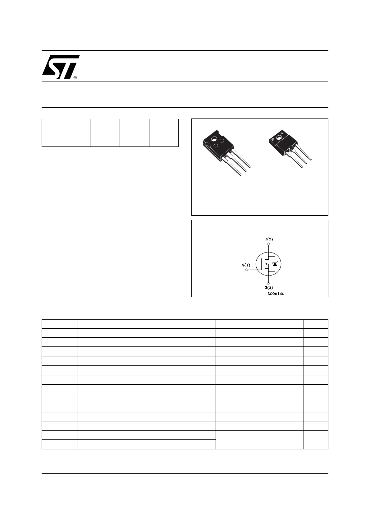
TO-247
3
2
1
ISOWATT218
INTERNAL SCHEMATIC DIAGRAM
3
ABSOLUTE MAXIMUM RATINGS
Symbol Parameter Value Unit
STW10NC60 STH10NC60FI
(1)
j
Drain-source Voltage (VGS = 0)
Drain-gate Voltage (RGS = 20 kΩ)
600 V
600 V
Gate- source Voltage ±30 V
Drain Current (continuous) at TC = 25°C
Drain Current (continuous) at TC = 100°C
10 10 (*) A
6.3 6.3 (*) A
Drain Current (pulsed) 40 40 (*) A
Total Dissipation at TC = 25°C
160 60 W
Derating Factor 1.28 0.48 W/°C
Insulation Withstand Voltage (DC) - 2500 V
Storage Temperature
Max. Operating Junction Temperature
(1)ISD ≤10A, di/dt ≤100A/µs, VDD ≤ V
(*) Limited only by Maximum Temperature Allowed
– 55 to 150 °C
, Tj ≤ T
(BR)DSS
JMAX
V
DS
V
DGR
V
GS
I
D
I
D
I
DM
P
TOT
dv/dt Peak Diode Recovery voltage slope 3.5 V/ns
V
ISO
T
stg
T
(•)Pu l se width limite d by safe operati ng area
.
1/9February 2002
Page 2
STW10NC60 / STH10NC60FI
THERMA L D ATA
TO-247 ISOWATT218
Rthj-case Thermal Resistance Junction-case Max 0.78 2.08 °C/W
Rthj-amb Thermal Resistance Junction-ambient Max 30 °C/W
T
AVALANCHE CHARACTERISTICS
Symbol Parameter Max Value Unit
I
AR
E
AS
ELECTRICAL CHARACTERISTICS (TCASE = 25 °C UNLESS OTHERWISE SPECIFIED)
OFF
Symbol Parameter Test Conditions Min. Typ. Max. Unit
V
(BR)DSS
I
DSS
I
GSS
Maximum Lead Temperature For Soldering Purpose 300 °C
l
Avalanche Current, Repetitive or Not-Repetitive
(pulse width limited by T
max)
j
Single Pulse Avalanche Energy
(starting T
= 25 °C, ID = IAR, VDD = 50 V)
j
Drain-source
Breakdown Voltage
Zero Gate Voltage
Drain Current (V
GS
= 0)
Gate-body Leakage
Current (V
DS
= 0)
10 A
820 mJ
ID = 250 µA, VGS = 0 600
V
= Max Rating
DS
V
= Max Rating, TC = 125 °C
DS
V
= ±30V ±100 nA
GS
1µA
50 µA
V
ON
(1)
Symbol Parameter Test Conditions Min. Typ. Max. Unit
V
V
GS(th)
R
DS(on)
Gate Threshold Voltage
Static Drain-source On
= VGS, ID = 250µA
DS
VGS = 10V, ID = 4.5 A
234V
0.6 0.75 Ω
Resistance
DYNAMIC
Symbol Parameter Test Conditions Min. Typ. Max. Unit
(1) Forward Transconductance VDS =20 V , ID=4.5A 9 S
g
fs
C
iss
C
oss
C
rss
Input Capacitance
Output Capacitance 205 pF
Reverse Transfer
Capacitance
V
= 25V, f = 1 MHz, VGS = 0
DS
1420 pF
35 pF
2/9
Page 3
STW10NC60 / STH10NC60FI
ELECTRICAL CHARACTERISTICS (CONTINUED)
SWITCHING ON
Symbol Parameter Test Conditions Min. Typ. Max. Unit
t
d(on)
Turn-on Delay Time VDD = 300V, ID = 4.5 A
RG=4.7Ω VGS = 10V
t
r
Q
g
Q
gs
Q
gd
Rise Time 16 ns
Total Gate Charge
Gate-Source Charge 4.5 nC
Gate-Drain Charge 31 nC
(see test circuit, Figure 3)
V
= 480V, ID = 9.0 A,
DD
V
= 10V
GS
SWITCHING OFF
Symbol Parameter Test Conditions Min. Typ. Max. Unit
t
d(off)
Turn-off Delay Time
t
f
Fall Time
VDD = 300 V, ID = 4.5 A
R
= 4.7Ω VGS = 10 V
G
(Resistive Load see, Figure 3)
t
r(Voff)
t
f
t
c
Fall Time
Cross-over Time
Off-voltage Rise Time
= 480V, ID = 9.0 A,
V
DD
RG= 4.7Ω, V
GS
= 10V
(Inductive Load see, Figure 5)
SOURCE DRAIN DIODE
Symbol Parameter Test Conditions Min. Typ. Max. Unit
I
SD
I
SDM
V
(1)
SD
t
rr
Q
rr
I
RRM
Note: 1. Pulsed: Puls e duration = 300 µs, duty cycle 1 .5 %.
2. Pulse width limited by safe operating area.
Source-drain Current 10 A
(2)
Source-drain Current (pulsed) 40 A
Forward On Voltage
Reverse Recovery Time
Reverse Recovery Charge 4.7 µC
ISD = 9 A, VGS = 0
I
= 9 A, di/dt = 100A/µs,
SD
VDD = 100V, Tj = 150°C
(see test circuit, Figure 5)
Reverse Recovery Current 15.5 A
20 ns
55 77 nC
64
32
19
13
32
1.6 V
600 ns
ns
ns
ns
ns
ns
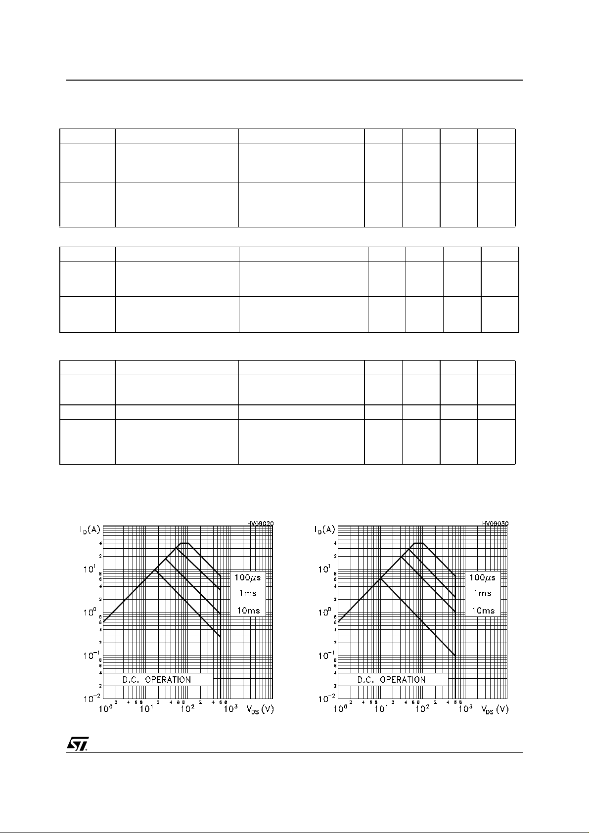
Safe Operating Area for ISOWATT218Safe Operating Area for TO-247
3/9
Page 4

STW10NC60 / STH10NC60FI
Thermal Impedance for ISOWATT218Thermal Impedance for TO-247
Output Characteristics Transfer Characteristics
Transco nductance
4/9
Static Drain-source On Resistance
Page 5

STW10NC60 / STH10NC60FI
Gate Charge vs Gate-source Voltage
Normalized Gate Thereshold Voltage vs Temp. Normalized On Resistance vs Temperature
Capacitance Variations
Source-drain Diode Forward Characteristics
5/9
Page 6

STW10NC60 / STH10NC60FI
Fig. 2: Unclamped Inductive WaveformFig. 1: Unclamped Inductive Load Test Circuit
Fig. 3: Switching Times Test Circuit For
Resistive Load
Fig. 5: Test Circuit For Inductive Load Switching
And Diode Recovery Times
Fig. 4: Gate Charge test Circuit
6/9
Page 7

TO-247 MECHANICAL DATA
STW10NC60 / STH10NC60FI
DIM.
A 4.85 5.15 0.19 0.20
D 2.20 2.60 0.08 0.10
E 0.40 0.80 0.015 0.03
F 1 1.40 0.04 0.05
F1 3 0.11
F2 2 0.07
F3 2 2.40 0.07 0.09
F4 3 3.40 0.11 0.13
G 10.90 0.43
H 15.45 15.75 0.60 0.62
L 19.85 20.15 0.78 0.79
L1 3.70 4.30 0.14 0.17
L2 18.50 0.72
L3 14.20 14.80 0.56 0.58
L4 34.60 1.36
L5 5.50 0.21
M 2 3 0.07 0.11
V
V2
Dia 3.55 3.65 0.14 0.143
MIN. TYP MAX. MIN. TYP. MAX.
mm. inch
5º5º
60º 60º
7/9
Page 8

STW10NC60 / STH10NC60FI
ISOWATT218 MECHANICAL DATA
DIM.
A 5.35 5.65 0.211 0.222
C 3.30 3.80 0.130 0.150
D 2.90 3.10 0.114 0.122
D1 1.88 2.08 0.074 0.082
E 0.75 0.95 0.030 0.037
F 1.05 1.25 0.041 0.049
F2 1.50 1.70 0.059 0.067
F3 1.90 2.10 0.075 0.083
G 10.80 11.20 0.425 0.441
H 15.80 16.20 0.622 0.638
L 9 0.354
L1 20.80 21.20 0.819 0.835
L2 19.10 19.90 0.752 0.783
L3 22.80 23.60 0.898 0.929
L4 40.50 42.50 1.594 1.673
L5 4.85 5.25 0.191 0.207
L6 20.25 20.75 0.797 0.817
N 2.1 2.3 0.083 0.091
R 4.6 0.181
DIA 3.5 3.7 0.138 0.146
MIN. TYP. MAX. MIN. TYP. MAX.
mm inch
8/9
- Weight : 4.9 g (typ.)
- Maximum Torque (applied to mounting flange) Recommended: 0.8 Nm; Maximum: 1 Nm
- The side of the dissipator must be flat within 80 µm
P025C/A
Page 9

STW10NC60 / STH10NC60FI
Information furnished is believed to be accurate and reliable. However, STMicroelectronics assumes no responsibility for the consequences
of use of such informa tion n or for an y infring ement of patent s or other rig hts of third part ies which may resu lt from its use . No l i cen se i s
granted by implication or otherwise under any patent or patent rights of STMicroelectronics. Specification mentioned in this publication are
subject to change without notice. This publication supersedes and replaces all information previously supplied. STMicroelectronics products
are not authorized for use as critical compo nents in life support devices or systems without express written approval of STMicroelectronics.
Australia - Brazil - China - Finland - France - Germany - Hong Kong - India - Italy - Japan - Malaysia - Malta - Morocco -
The ST logo is a trademark of STMicroelectronics
© 2001 STMicroelectronics – Printed in Italy – All Rights Reserved
STMicroelectronics GROUP OF COMPANIES
Singapore - Spain - Sweden - Switzerland - United Kingdom - U.S.A.
http://www.st.com
9/9
 Loading...