

Page 1
STH10NA50/FI
STW10NA50
N - CHANNEL ENHANCEMENT MODE
FAST POWER MOS TRANSISTOR
TYPE V
STH 10NA50
STH 10NA50FI
STW10NA50
■ TYPICAL R
■ ± 30V GATE TO SOURCE VOLTAGE RATING
■ 100% AVALANCHE TESTED
■ REPETITIVE AVALANCHE DATA AT 100
■ LOW INTRINSIC CAPACITANCES
■ GATE GHARGE MINIMIZED
■ REDUCED THRESHOLD VOLTAGE SPREAD
DS(on)
DSS
500 V
500 V
500 V
= 0.7 Ω
R
DS(on)
<0.8Ω
<0.8Ω
<0.8Ω
I
D
9.6 A
5.6 A
9.6 A
o
C
DESCRIPTION
This series of POWER MOSFETS represents the
most advanced high voltage technology. The
optimized cell layout coupled with a new
proprietary edge termination concur to give the
device low R
and gate charge, unequalled
DS(on)
ruggedness and superior switching performance.
APPLICATIONS
■ HIGH CURRENT, HIGH SPEED SWITCHING
■ SWITCH MODE POWERSUPPLIES (SMPS)
■ DC-AC CONVERTERS FOR WELDING
EQUIPMENT AND UNINTERRUPTIBLE
POWER SUPPLIES AND MOTOR DRIVE
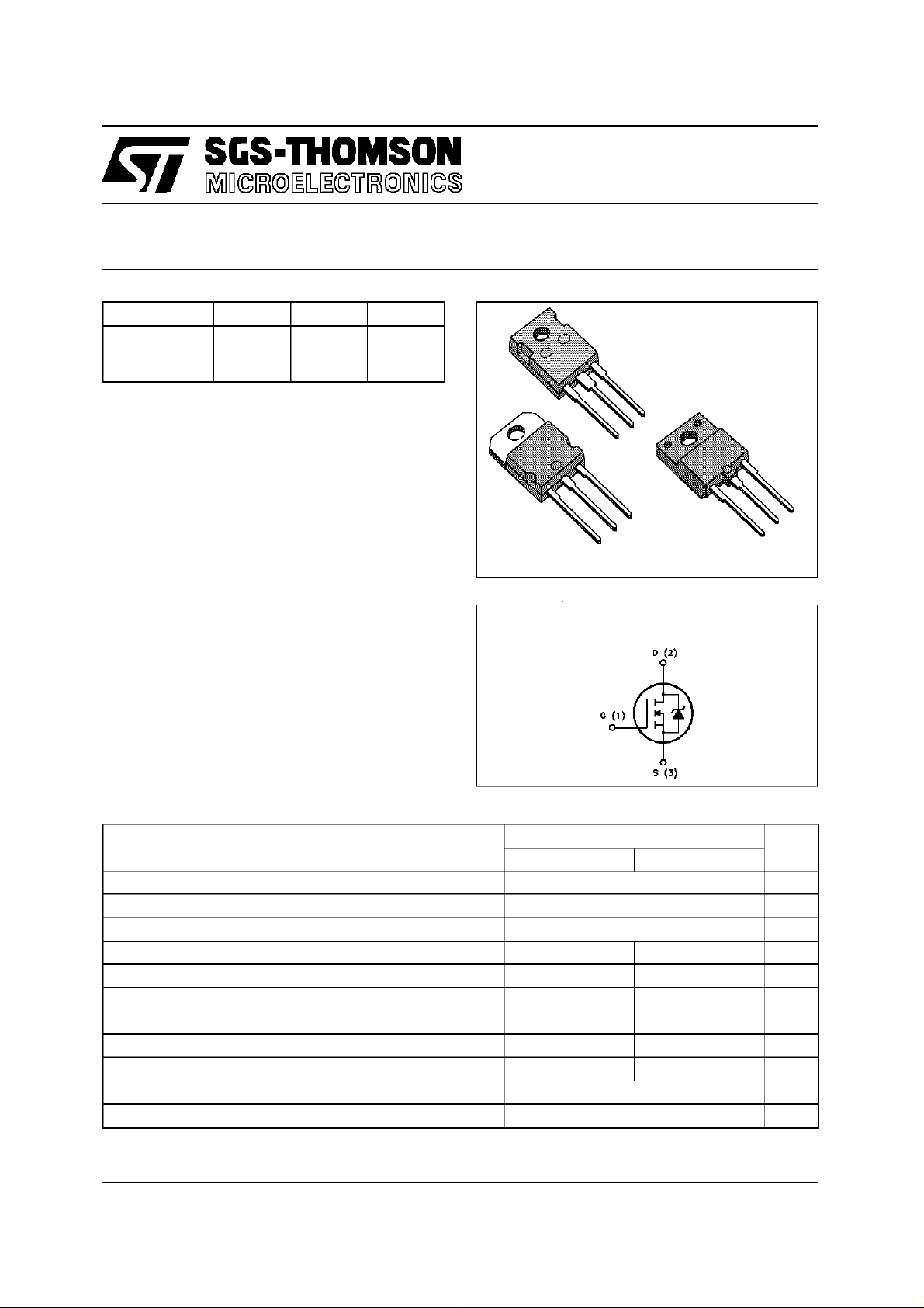
TO-247
3
2
1
3
2
TO-218 ISOWATT218
1
INTERNAL SCHEMATIC DIAGRAM
3
2
1
ABSOLUTE MAXIMUM RATINGS
Symb o l Paramet er Val u e Unit
STW/STH10NA50 STH10NA50FI
V
V
V
I
DM
P
V
T
(•) Pulsewidth limited bysafe operating area
November 1996
Drain - s ource Voltage (VGS=0) 500 V
DS
Drain - gat e Voltage (RGS=20kΩ)500V
DGR
Gate-source Voltage ± 30 V
GS
Drain Current (continuous) at Tc=25oC9.65.6A
I
D
Drain Current (continuous) at Tc=100oC6.1 3.5A
I
D
(•) Drain Current (pulsed) 38 38 A
Total Di ssipation a t Tc=25oC 150 60 W
tot
Derat ing Factor 1.2 0.48 W/
Ins ulation Withs t and Voltage (DC) 4000 V
ISO
St or a ge Tem perature -65 t o 150
stg
Max. Operating Jun ction T emperature 150
T
j
o
o
o
C
C
C
1/11
Page 2

STH10NA50/FI STW10NA50
THERMAL DATA
TO - 218/ TO-247 IS OWATT218
R
thj-case
R
thj-amb
R
thc-sink
T
AVALANCHE CHARACTERISTICS
Symbol Parameter Max Value Uni t
I
AR
E
E
I
AR
Thermal Resistance J unction- c ase Max 0.83 2.08
Thermal Resistance Junc tion-am bie nt Max
Thermal Resistance Cas e-sink Typ
Maximum Lead Temperature For So ldering Purpose
l
Avalanc h e Cu rr ent , Repet itive or Not-Rep etitive
(pulse width limited by Tjmax, δ <1%)
Single Pul se Avalanche Ener gy
AS
(starti ng T
Repetitive Avalanc he Energ y
AR
=25oC, ID=IAR,VDD=50V)
j
(pulse width limited by Tjmax, δ <1%)
Avalanc h e Cu rr ent , Repet itive or Not-Rep etitive
(Tc= 100oC, pulse width l imited by Tjmax, δ <1%)
30
0.1
300
9.6 A
460 mJ
16 mJ
5.6 A
o
C/W
o
C/W
o
C/W
o
C
ELECTRICAL CHARACTERISTICS (T
=25oC unless otherwisespecified)
case
OFF
Symbol Parameter Te st Conditions Min. Typ. Max. Unit
V
(BR)DSS
Drain - s ource
ID=250µAVGS= 0 500 V
Break d own Volta ge
I
DSS
I
GSS
Zer o G at e V oltage
Drain Current (VGS=0)
Gat e- body Leakage
Current (V
DS
=0)
VDS=MaxRating
VDS= Max Rating x 0.8 Tc=125oC
= ± 30 V ± 10 0 nA
V
GS
25
250
ON (∗)
Symbol Parameter Te st Conditions Min. Typ. Max. Unit
V
GS(th)
R
DS(on)
Gate Threshold V oltage VDS=VGSID=250µA 2.25 3 3.75 V
St at ic Drain-s our ce O n
VGS=10V ID=5A 0.7 0.8 Ω
Resistance
I
D(on)
On State Drain Current VDS>I
D(on)xRDS(on)max
10 A
VGS=10V
DYNAMIC
Symbol Parameter Te st Conditions Min. Typ. Max. Unit
(∗)Forward
g
fs
Tr ansconductance
C
C
C
Input Capacitance
iss
Out put Capacitance
oss
Reverse Transfer
rss
Capacitance
VDS>I
D(on)xRDS(on)maxID
=45A 4.5 7.4 S
VDS=25V f=1MHz VGS= 0 1350
200
50
1800
270
70
µA
µA
pF
pF
pF
2/11
Page 3
STH10NA50/FI STW10NA50
ELECTRICAL CHARACTERISTICS (continued)
SWITCHING ON
Symbol Parameter Te st Conditions Min. Typ. Max. Unit
t
d(on)
(di/dt)
Q
Q
Q
Turn-on T ime
t
Rise Time
r
Turn-on Current S lope VDD=400V ID=10A
on
Total Gate Charge
g
Gat e- Source Charge
gs
Gate-Drain Charge
gd
SWITCHING OFF
Symbol Parameter Te st Conditions Min. Typ. Max. Unit
t
r(Voff)
t
Off -voltage Rise Time
t
Fall Time
f
Cross-over Time
c
SOURCE DRAINDIODE
VDD=250V ID=5A
RG=4.7 Ω VGS=10V
18
25
(see test circuit, figure 3)
200 A/µs
RG=47 Ω VGS=10V
(see test circuit, figure 5)
VDD= 400 V ID=10A VGS=10V 56
9
26
VDD=400V ID=10A
RG=4.7 Ω VGS=10V
(see test circuit, figure 5)
15
15
25
25
35
75 nC
20
20
35
ns
ns
nC
nC
ns
ns
ns
Symbol Parameter Te st Conditions Min. Typ. Max. Unit
I
I
SDM
SD
Source-drain C urrent
(•)
Source-drain C urrent
9.6
38
(pulsed)
V
(∗) F or ward On Voltage ISD=10A VGS=0 1.6 V
SD
t
Reverse Recovery
rr
Time
Q
Reverse Recovery
rr
ISD= 10 A di/dt = 100 A/µs
VDD= 100 V Tj=150oC
(see test circuit, figure 5)
560
9
Charge
I
RRM
Reverse Recovery
32
Current
(∗) Pulsed:Pulse duration = 300 µs, dutycycle 1.5 %
(•) Pulse widthlimited by safeoperating area
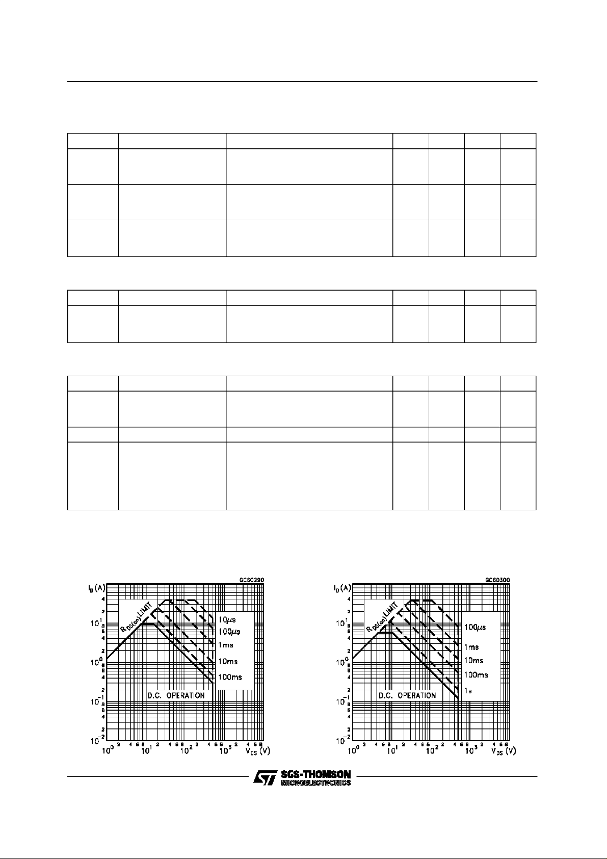
Safe Operating Areas for TO-218 and TO-247 Safe Operating Areas forISOWATT218
A
A
ns
µC
A
3/11
Page 4
STH10NA50/FI STW10NA50
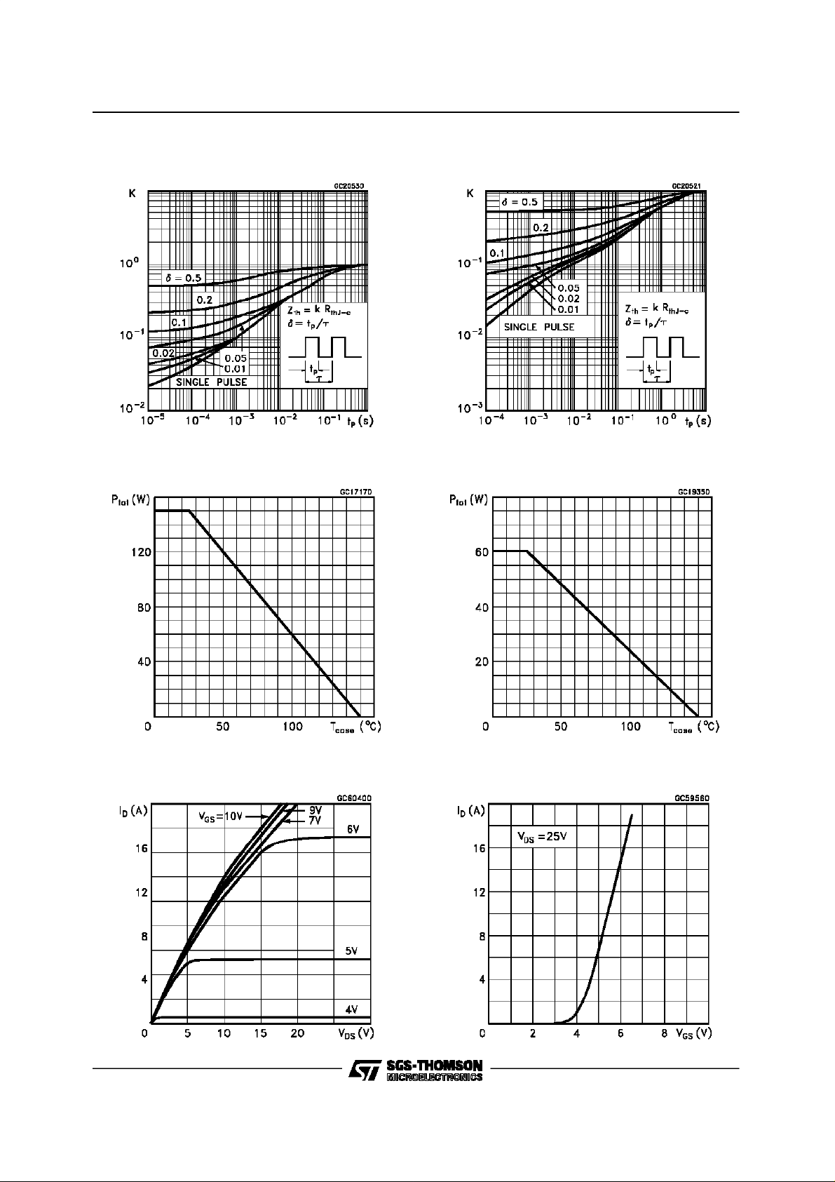
Thermal ImpedeanceFor TO-218
Derating Curve For TO-218
Thermal ImpedanceFor ISOWATT218
Derating Curve For ISOWATT218
Output Characteristics
4/11
Transfer Characteristics
Page 5

STH10NA50/FI STW10NA50
Transconductance Static Drain-source On Resistance
Gate Charge vs Gate-source Voltage Capacitance Variations
Temperature
Normalized On Resistance vs TemperatureNormalized Gate Threshold Voltage vs
5/11
Page 6

STH10NA50/FI STW10NA50
Turn-on Current Slope Turn-off Drain-source Voltage Slope
Cross-over Time Switching Safe Operating Area
Accidental Overload Area Source-drain Diode ForwardCharacteristics
6/11
Page 7

STH10NA50/FI STW10NA50
Fig. 1: Unclamped Inductive Load Test Circuits
Fig. 3: Switching Times Test Circuits For
Resistive Load
Fig. 2: Unclamped Inductive Waveforms
Fig. 4: Gate Charge Test Circuit
Fig. 5: Test Circuit For Inductive Load Switching
And Diode Reverse Recovery Time
7/11
Page 8

STH10NA50/FI STW10NA50
TO-247 MECHANICAL DATA
DIM.
MIN. TYP. MAX. MIN. TYP. MAX.
A 4.7 5.3 0.185 0.208
A1 2.87 0.113
A2 1.5 2.5 0.059 0.098
b 1 1.4 0.039 0.055
b1 2.25 0.088
b2 3.05 3.43 0.120 0.135
C 0.4 0.8 0.015 0.031
D 20.4 21.18 0.803 0.833
e 5.43 5.47 0.213 0.215
E 15.3 15.95 0.602 0.628
L 15.57 0.613
L1 3.7 4.3 0.145 0.169
Q 5.3 5.84 0.208 0.230
ØP 3.5 3.71 0.137 0.146
mm inch
8/11
C
A
b1
A1
b
e
b2
A2
Q
D
L1
L
ø
E
Page 9

STH10NA50/FI STW10NA50
TO-218 (SOT-93) MECHANICAL DATA
DIM.
MIN. TYP. MAX. MIN. TYP. MAX.
A 4.7 4.9 0.185 0.193
C 1.17 1.37 0.046 0.054
D 2.5 0.098
E 0.5 0.78 0.019 0.030
F 1.1 1.3 0.043 0.051
G 10.8 11.1 0.425 0.437
H 14.7 15.2 0.578 0.598
L2 – 16.2 – 0.637
L3 18 0.708
L5 3.95 4.15 0.155 0.163
L6 31 1.220
R – 12.2 – 0.480
Ø 4 4.1 0.157 0.161
mm inch
E
A
C
L5
D
L6
L3
L2
H
G
Ø
F
R
123
P025A
9/11
Page 10

STH10NA50/FI STW10NA50
ISOWATT218 MECHANICAL DATA
DIM.
mm inch
MIN. TYP. MAX. MIN. TYP. MAX.
A 5.35 5.65 0.210 0.222
C 3.3 3.8 0.130 0.149
D 2.9 3.1 0.114 0.122
D1 1.88 2.08 0.074 0.081
E 0.45 1 0.017 0.039
F 1.05 1.25 0.041 0.049
G 10.8 11.2 0.425 0.441
H 15.8 16.2 0.622 0.637
L1 20.8 21.2 0.818 0.834
L2 19.1 19.9 0.752 0.783
L3 22.8 23.6 0.897 0.929
L4 40.5 42.5 1.594 1.673
L5 4.85 5.25 0.190 0.206
L6 20.25 20.75 0.797 0.817
M 3.5 3.7 0.137 0.145
N 2.1 2.3 0.082 0.090
U 4.6 0.181
L3
N
E
A
D
C
L5
M
H
L2
L6
L1
D1
L4
F
U
G
123
P025C
10/11
Page 11

STH10NA50/FI STW10NA50
Information furnished is believed to be accurate and reliable. However, SGS-THOMSON Microelectronics assumes no responsability for the
consequences of use of such informationnor for any infringement of patents or other rightsof third parties which may results fromits use. No
licenseis grantedby implication orotherwise underany patent or patentrights ofSGS-THOMSONMicroelectronics. Specificationsmentioned
in thispublication aresubject tochangewithoutnotice. Thispublicationsupersedes and replacesall informationpreviously supplied.
SGS-THOMSONMicroelectronics products are not authorizedfor use ascriticalcomponents in lifesupport devices or systems without express
writtenapproval ofSGS-THOMSONMicroelectonics.
1996 SGS-THOMSON Microelectronics - Printedin Italy- AllRightsReserved
Australia- Brazil -Canada -China - France- Germany - HongKong- Italy- Japan- Korea- Malaysia -Malta - Morocco - TheNetherlands -
Singapore - Spain- Sweden- Switzerland -Taiwan - Thailand- UnitedKingdom - U.S.A
SGS-THOMSONMicroelectronics GROUP OFCOMPANIES
.
11/11
 Loading...