

Page 1
STD12N05L
STD12N06L
N - CHANNEL ENHANCEMENT MODE
LOW THRESHOLD POWER MOS TRANSISTOR
TYPE V
DSS
R
DS(on)
I
D
STD 12N05L 50 V < 0.15 Ω 12 A
STD 12N06L 60 V < 0.15 Ω 12 A
■ TYPICAL R
■ AVALANCHE RUGGED TECHNOLOGY
■ 100% AVALANCHE TESTED
■ REPETITIVE AVALANCHE DATA AT 100
■ LOW GATE CHARGE
■ LOGIC LEVEL COMPATIBLE INPUT
o
■ 175
■ APPLICATION ORIENTED
C OPERATING TEMPERATURE
DS(on)
= 0.115 Ω
o
C
CHARACTERIZATION
■ THROUGH-HOLE IPAK (TO-251) POWER
PACKAGE IN TUBE (SUFFIX ”-1”)
■ SURFACE-MOUNTINGDPAK (TO-252)
POWER PACKAGE IN TAPE & REEL
(SUFFIX ”T4”)
APPLICATIONS
■ HIGH CURRENT, HIGH SPEED SWITCHING
■ SOLENOID AND RELAY DRIVERS
■ REGULATORS
■ DC-DC & DC-AC CONVERTERS
■ MOTOR CONTROL, AUDIO AMPLIFIERS
■ AUTOMOTIVE ENVIRONMENT (INJECTION,
ABS, AIR-BAG, LAMPDRIVERS, Etc.)
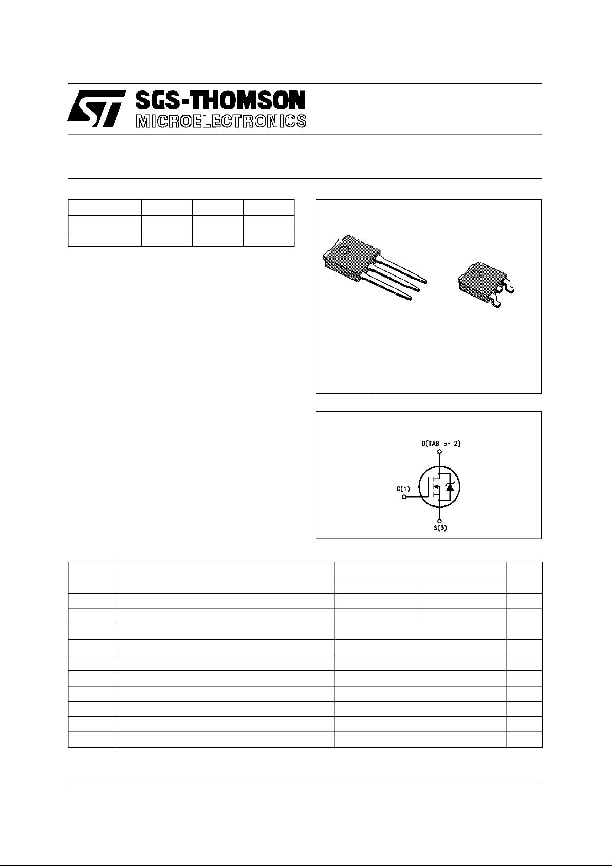
3
2
1
IPAK
TO-251
(Suffix ”-1”)
INTERNAL SCHEMATIC DIAGRAM
1
DPAK
TO-252
(Suffix ”T4”)
3
ABSOLUTE MAXIMUM RATINGS
Symb o l Paramet er Val u e Unit
STD 12N05L STD12N06L
V
V
V
I
DM
P
T
(•) Pulsewidth limited bysafe operating area
November 1996
Drain - s ource Voltage (VGS=0) 50 60 V
DS
Drain- gate Voltage (RGS=20kΩ)5060V
DGR
Gate-source Voltage ± 15 V
GS
Drain Current (continuous) at Tc=25oC12A
I
D
Drain Current (continuous) at Tc=100oC8A
I
D
(•) Drain Current (pulsed) 48 A
Total D i ssipation at Tc=25oC45W
tot
Derating Factor 0.3 W/
St or a ge Tem perature -65 to 175
stg
Max. Operating Junctio n Temperatur e 175
T
j
o
o
o
C
C
C
1/10
Page 2

STD12N05L/STD12N06L
THERMAL DATA
R
thj-case
R
thj-amb
R
thc-sink
T
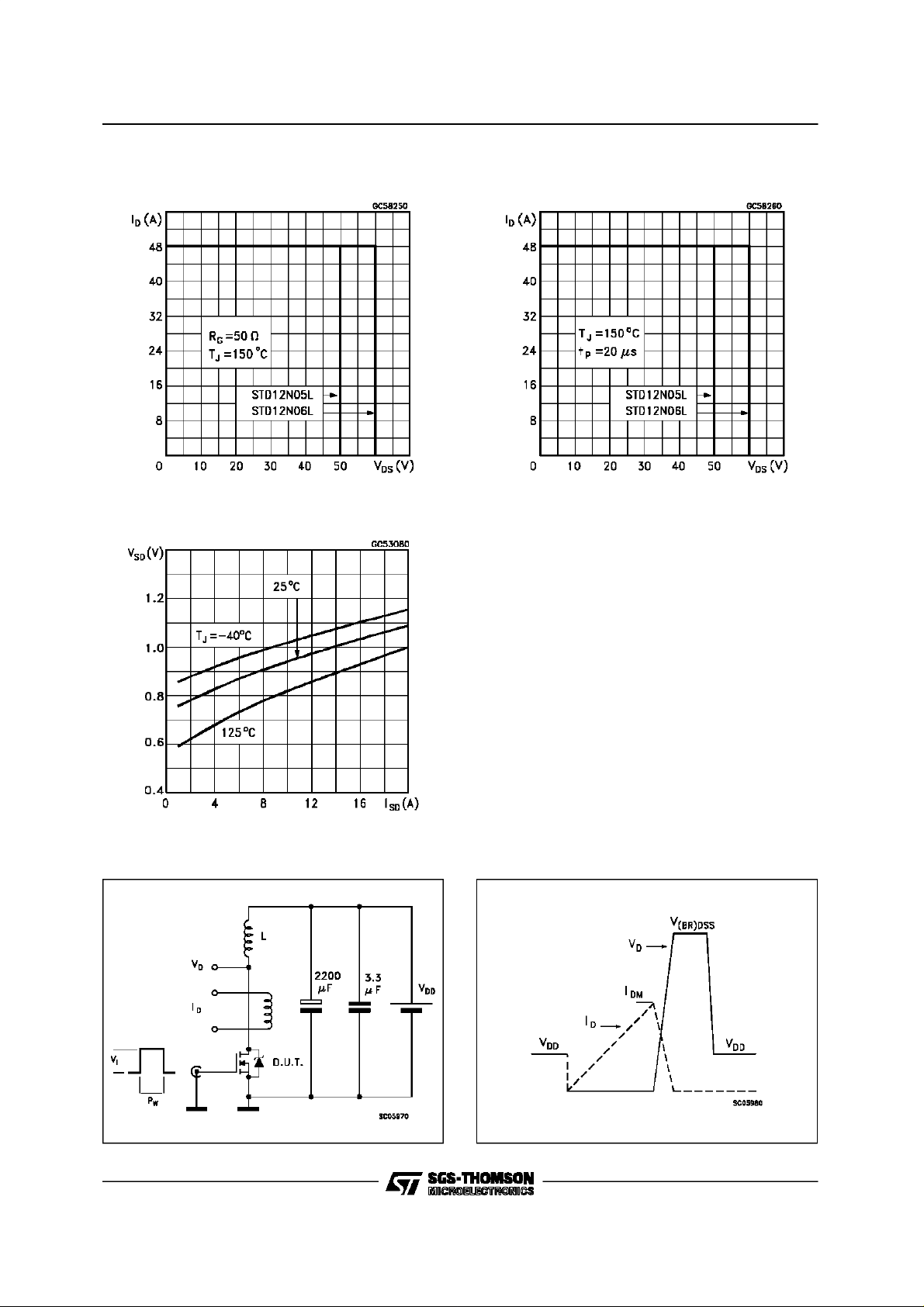
AVALANCHE CHARACTERISTICS
Symbol Parameter Max Value Uni t
I
AR
E
E
I
AR
Thermal Resistance Junction - cas e Max
Thermal Resistance Junction- ambient Max
Thermal Resistance Case-sink Typ
Maximum L ead Temperat ur e For Soldering Purpos e
l
Avalanc h e Cu rr ent , Repet itive or Not-R epetitive
(pulse width limited by Tjmax, δ <1%)
Single Pul se Avalanche Ener gy
AS
(starti ng Tj=25oC, ID=IAR,VDD=25V)
Repetitive Avalanc he Energ y
AR
(pulse width limited by Tjmax, δ <1%)
Avalanc h e Cu rr ent , Repet itive or Not-R epetitive
(Tc= 100oC, puls e width limited by Tjmax, δ <1%)
3.33
100
1.5
275
12 A
30 mJ
7mJ
8A
o
C/W
o
C/W
o
C/W
o
C
ELECTRICAL CHARACTERISTICS (T
=25oC unless otherwise specified)
case
OFF
Symbol Parameter Test Condition s Min. Typ. Max. Unit
V
(BR)DSS
I
DSS
I
GSS
Drain - s ource
Break d own Volta ge
Zer o Gate Voltage
Drain Current (VGS=0)
Gat e- body Leakage
ID=250µAVGS=0
for STD12N05 L
for STD12N06 L
VDS=MaxRating
VDS= Max R ating x 0.8 Tc=125oC
50
60
1
10
VGS= ± 15 V ± 100 nA
Current (VDS=0)
ON (∗)
Symbol Parameter Test Condition s Min. Typ. Max. Unit
V
GS(th)
R
DS(on)
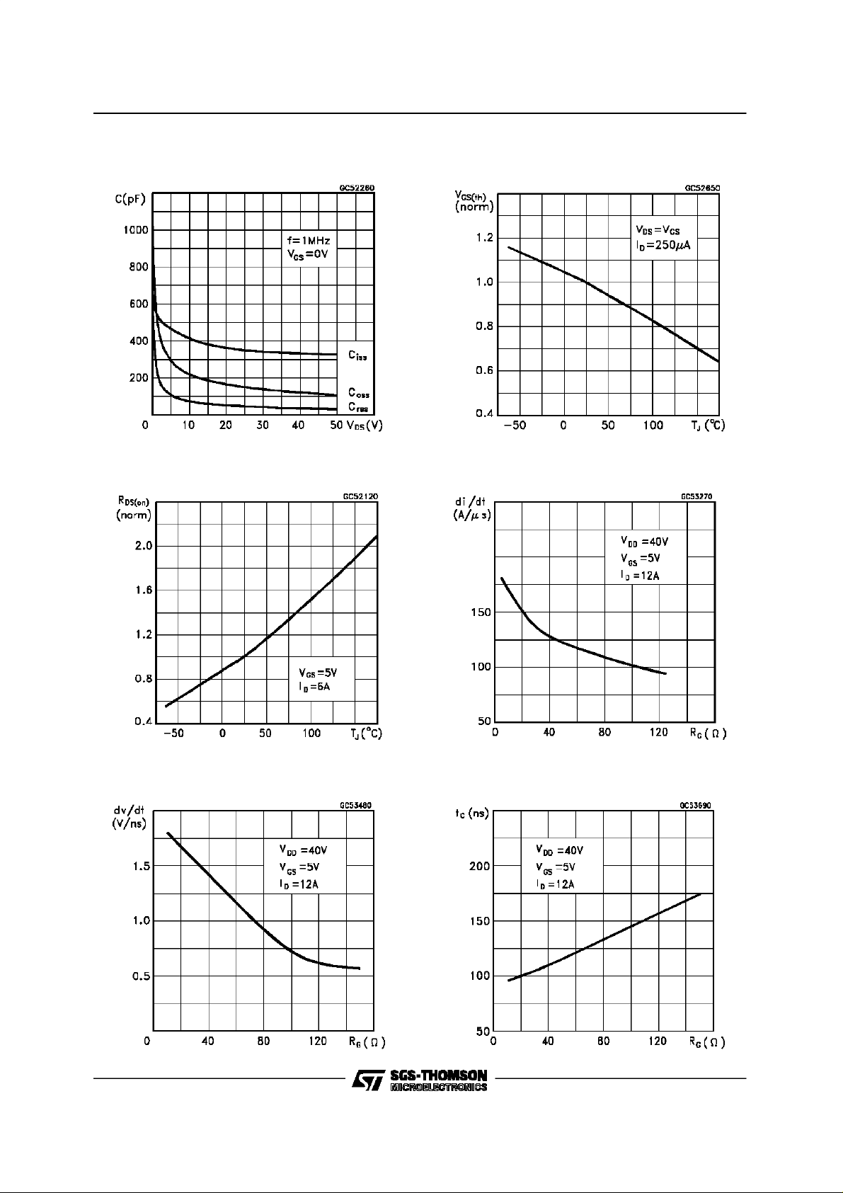
Gate Threshold Voltage VDS=VGSID=250µA11.62.5V
St at ic Drain-s our ce O n
VGS=5 V ID=6A 0.115 0.15 Ω
Resistance
I
D(on)
On St ate Dra in Current VDS>I
D(on)xRDS(on)max
12 A
VGS=10 V
DYNAMIC
Symbol Parameter Test Condition s Min. Typ. Max. Unit
(∗)Forward
g
fs
Tr ansconductance
C
C
C
Input Capacitance
iss
Out put Capacitance
oss
Reverse Transfer
rss
Capacitance
VDS>I
D(on)xRDS(on)maxID
=6A 4 8 S
VDS=25V f=1MHz VGS=0 350
150
50
500
200
80
V
V
µA
µA
pF
pF
pF
2/10
Page 3

STD12N05L/STD12N06L
ELECTRICAL CHARACTERISTICS (continued)
SWITCHING ON
Symbol Parameter Test Condition s Min. Typ. Max. Unit
t
d(on)
(di/dt)
Q
Q
Q
Turn-on Time
t
Rise Time
r
Turn-on C urrent Slope VDD=40V ID=12A
on
Total Gate Charge
g
Gat e- Source Charge
gs
Gate-Drain Charge
gd
SWITCHING OFF
Symbol Parameter Test Condition s Min. Typ. Max. Unit
t
r(Voff)
t
Off -voltage R ise Time
t
Fall Time
f
Cross-over Time
c
SOURCE DRAIN DIODE
VDD=25V ID=6A
RG=50 Ω VGS=5V
55
18080260
(see test circuit, figure 3)
120 A/µs
RG=50 Ω VGS=5V
(see test circuit, figure 5)
VDD=40V ID=12A VGS=5V 12
6
5
VDD=40V ID=12A
RG=50 Ω VGS=5V
(see test circuit, figure 5)
40
60
110
18 nC
60
90
160
ns
ns
nC
nC
ns
ns
ns
Symbol Parameter Test Condition s Min. Typ. Max. Unit
I
I
SDM
SD
Source-drain Current
(•)
Source-drain Current
12
48
(pulsed)
V
(∗) F or w ar d On Volt age ISD=12A VGS=0 1.5 V
SD
t
Reverse Recovery
rr
Time
Q
Reverse Recovery
rr
ISD= 12 A di/dt = 100 A/µs
VDD=25V Tj=150oC
(see test circuit, figure 5)
75
0.15
Charge
I
RRM
Reverse Recovery
4
Current
(∗) Pulsed:Pulse duration = 300 µs, dutycycle 1.5 %
(•) Pulse widthlimited by safeoperating area
Safe Operating Areas Thermal Impedance
A
A
ns
µC
A
3/10
Page 4

STD12N05L/STD12N06L
Derating Curve
Transfer Characteristics
Output Characteristics
Transconductance
Static Drain-source On Resistance
4/10
Gate Charge vs Gate-source Voltage
Page 5
STD12N05L/STD12N06L
Capacitance Variations Normalized Gate Threshold Voltage vs
Temperature
Normalized On Resistance vs Temperature Turn-on Current Slope
Cross-over TimeTurn-off Drain-source Voltage Slope
5/10
Page 6
STD12N05L/STD12N06L
Switching SafeOperating Area Accidental Overload Area
Source-drain Diode Forward Characteristics
Fig. 1: Unclamped Inductive Load Test Circuits Fig. 2: Unclamped Inductive Waveforms
6/10
Page 7

STD12N05L/STD12N06L
Fig. 3: Switching Times Test Circuits For
Resistive Load
Fig. 5: Test Circuit For Inductive Load Switching
And Diode Reverse Recovery Time
Fig. 4: Gate Charge Test Circuit
7/10
Page 8

STD12N05L/STD12N06L
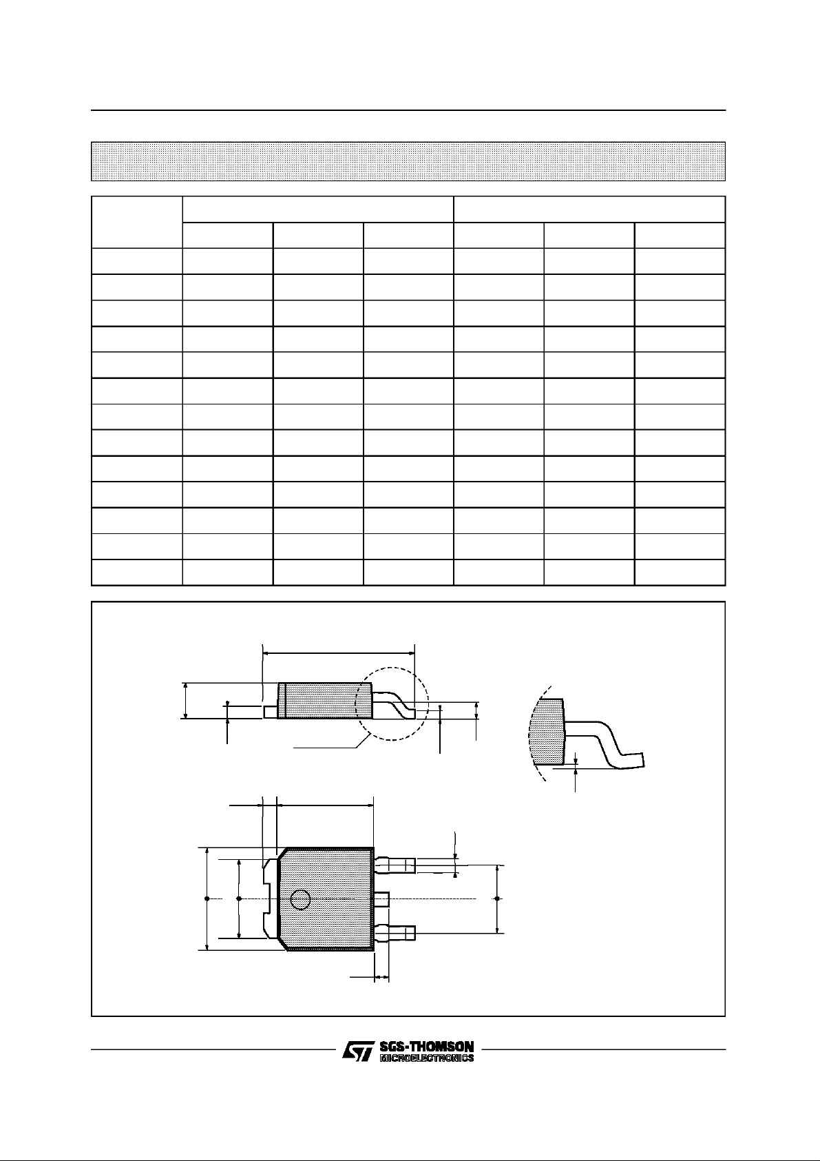
TO-251 (IPAK) MECHANICAL DATA
DIM.
mm inch
MIN. TYP. MAX. MIN. TYP. MAX.
A 2.2 2.4 0.086 0.094
A1 0.9 1.1 0.035 0.043
A3 0.7 1.3 0.027 0.051
B 0.64 0.9 0.025 0.031
B2 5.2 5.4 0.204 0.212
B3 0.85 0.033
B5 0.3 0.012
B6 0.95 0.037
C 0.45 0.6 0.017 0.023
C2 0.48 0.6 0.019 0.023
D 6 6.2 0.236 0.244
E 6.4 6.6 0.252 0.260
G 4.4 4.6 0.173 0.181
H 15.9 16.3 0.626 0.641
L 9 9.4 0.354 0.370
L1 0.8 1.2 0.031 0.047
L2 0.8 1 0.031 0.039
8/10
A
E
==
C2
L2
B2
==
H
C
A3
A1
B6
L
B
B5
G
==
D
B3
2
13
L1
0068771-E
Page 9
TO-252 (DPAK)MECHANICAL DATA
STD12N05L/STD12N06L
DIM.
mm inch
MIN. TYP. MAX. MIN. TYP. MAX.
A 2.2 2.4 0.086 0.094
A1 0.9 1.1 0.035 0.043
A2 0.03 0.23 0.001 0.009
B 0.64 0.9 0.025 0.035
B2 5.2 5.4 0.204 0.212
C 0.45 0.6 0.017 0.023
C2 0.48 0.6 0.019 0.023
D 6 6.2 0.236 0.244
E 6.4 6.6 0.252 0.260
G 4.4 4.6 0.173 0.181
H 9.35 10.1 0.368 0.397
L2 0.8 0.031
L4 0.6 1 0.023 0.039
H
A
E
==
C2
L2
B2
==
DETAIL”A”
D
2
13
L4
A1
C
A2
DETAIL”A”
B
G
==
0068772-B
9/10
Page 10

STD12N05L/STD12N06L
Information furnished is believed to be accurate and reliable. However, SGS-THOMSON Microelectronics assumes no responsability for the
consequences of useof such information nor for any infringement of patents or other rightsof third partieswhich may resultsfrom its use.No
licenseis granted by implication orotherwise underany patent or patentrights ofSGS-THOMSONMicroelectronics. Specifications mentioned
in thispublication are subject to change withoutnotice. Thispublication supersedes andreplacesall informationpreviouslysupplied.
SGS-THOMSONMicroelectronics products are not authorizedfor use ascriticalcomponents in lifesupportdevices orsystemswithout express
writtenapproval ofSGS-THOMSONMicroelectonics.
1996 SGS-THOMSON Microelectronics -Printed in Italy- AllRightsReserved
Australia- Brazil -Canada -China - France- Germany - HongKong- Italy - Japan- Korea- Malaysia - Malta- Morocco - The Netherlands -
Singapore - Spain - Sweden - Switzerland-Taiwan - Thailand- UnitedKingdom - U.S.A
SGS-THOMSONMicroelectronics GROUPOF COMPANIES
.
10/10
 Loading...