

Page 1
STD10PF06
P - CHANNEL 60V - 0.18 Ω - 10A TO-252
STripFET POWER MOSFET
TYPE V
DSS
R
DS(o n)
I
D
ST D10PF06 60 V < 0. 20 Ω 10 A
■ TYPICALR
■ EXCEPTIONALdv/dt CAPABILITY
■ 100%AVALANCHETESTED
■ LOW GATE CHARGE
■ APPLICATIONORIENTED
DS(on)
= 0.18 Ω
CHARACTERIZATION
■ ADDSUFFIX ”T4” FORORDERING IN TAPE
& REEL
DESCRIPTION
This Power MOSFET is the latest developmentof
STMicroelectronics unique ”Single Feature
Size” strip-based process. The resulting transi-
stor shows extremely high packing density for low
on-resistance, rugged avalanche characteristics
and less critical alignment steps therefore a remarkablemanufacturingreproducibility.
APPLICATIONS
■ MOTORCONTROL
■ DC-DC& DC-AC CONVERTERS
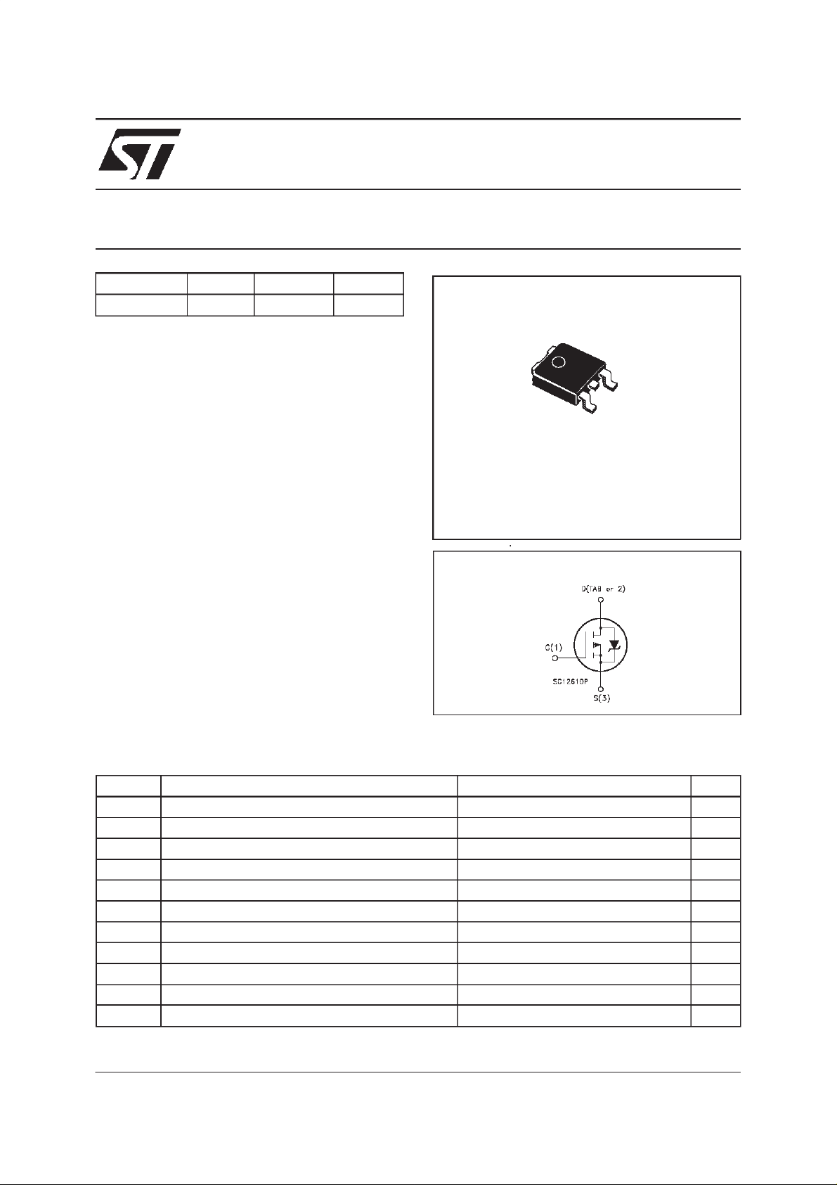
3
1
DPAK
TO-252
(Suffix ”T4”)
INTERNAL SCHEMATIC DIAGRAM
ABSOLUTE MAXIMUM RATINGS
Symbol Parameter Value Uni t
V
V
V
I
DM
P
dv/ d t Peak Diode Recover y volta ge s lope 6 V / ns
T
(•) Pulse width limited by safe operating area (1)I
Note:For the P-CHANNEL MOSFET actual polarity of voltages and current has to be reversed
April 1999
Drain-source Voltage (VGS=0) 60 V
DS
Drain- gat e Volt age (RGS=20kΩ)60V
DGR
Gate-source Voltage
GS
I
Drain Current (cont inuous) at Tc=25oC10A
D
I
Drain Current (cont inuous) at Tc=100oC7A
D
20 V
±
(•) Drain Current (pulsed) 40 A
Total Dissipation at Tc=25oC40W
tot
Derat ing Fac tor 0.27 W/
Sto rage T emperature -65 t o 175
stg
T
Max. Opera ti ng Junction Tempe r at ure 175
j
≤
10 A, di/dt≤300A/µs, V
SD
DD
≤
V
(BR)DSS,Tj
≤
T
JMAX
o
C
o
C
o
C
1/8
Page 2

STD10PF06
THERMAL DATA
R
thj-case
R
thj-amb
R
thc-sink
T
AVALANCHE CHARACTERISTICS
Symbol Parameter Max Value Unit
I
AR
E
Ther mal Resistanc e Junct ion-case Max
Ther mal Resistanc e Junct ion-ambient Max
Ther mal Resistanc e Case-sink Ty p
Maximum Lead Te m perature For So lder ing Purpos e
l
Avalanche Current, Repetitive or Not-Repetitive
(pulse width limited by T
Single Pulse A valanche E ner gy
AS
(starting T
=25oC, ID=IAR,VDD=25V)
j
max)
j
3.75
100
1.5
275
10 A
50 mJ
o
C/W
o
C/W
o
C/W
o
C
ELECTRICAL CHARACTERISTICS
=25oC unless otherwisespecified)
(T
case
OFF
Symbol Parameter Test Condit ions Min. Typ. M ax. Unit
V
(BR)DSS
Drain-source
ID=250µAVGS=0 60 V
Break dow n Volt age
I
DSS
I
GSS
Zero Gate Voltage
Drain Current (V
GS
Gat e- bod y Leakag e
Current (V
DS
=0)
=0)
V
=MaxRating
DS
=MaxRating Tc= 125oC
V
DS
V
=± 20 V
GS
1
10
100 nA
±
ON(∗)
Symbol Parameter Test Condit ions Min. Typ. M ax. Unit
V
GS(th)
R
DS(on)
Gate Threshold Voltage VDS=VGSID= 250 µA23.44V
Sta t ic Dr ain -s ource O n
VGS=10V ID= 5 A 0.18 0.20
Resistance
I
D(on)
On State Drain Current VDS>I
D(on)xRDS(on )max
10 A
VGS=10V
DYNAMIC
Symbol Parameter Test Condit ions Min. Typ. M ax. Unit
g
(∗)Forward
fs
Tr ansc on duc tance
C
C
C
Input C apac i t ance
iss
Out put Capacit ance
oss
Reverse T r ansfer
rss
Capacit a nc e
VDS>I
D(on)xRDS(on )maxID
=5A 2 5 S
VDS=25V f=1MHz VGS= 0 850
230
75
µ
µA
Ω
pF
pF
pF
A
2/8
Page 3

STD10PF06
ELECTRICAL CHARACTERISTICS
(continued)
SWITCHINGON
Symbol Parameter Test Condit ions Min. Typ. M ax. Unit
t
d(on)
Tur n-on Delay T ime
Rise T i me
t
r
VDD=30V ID=6A
R
=4.7
G
Ω
VGS=10V
20
40
(Resis t iv e Load, see f ig. 3)
Q
Q
Q
Tot al G at e Char ge
g
Gat e- Source Charge
gs
Gate-Drain Charge
gd
VDD=48V ID=12A VGS=10V 16
4
6
21 nC
SWITCHINGOFF
Symbol Parameter Test Condit ions Min. Typ. M ax. Unit
t
d(off)
Tur n-of f Delay Time
t
Fall T ime
f
VDD=30V ID=6A
=4.7 Ω VGS=10V
R
G
40
10
(Resis t iv e Load, see f ig. 3)
t
r(Voff)
t
t
Off-volt ag e Rise Time
Fall T ime
f
Cross-over Time
c
VDD=48V ID=12A
=4.7 Ω VGS=10V
R
G
(Indu ct iv e L oad , see fig . 5)
10
17
30
SOURCEDRAINDIODE
Symbol Parameter Test Condit ions Min. Typ. M ax. Unit
I
V
I
SDM
SD
Q
I
RRM
SD
t
Source-drain Current
(•)
Source-drain Current
10
40
(pulsed)
(∗)ForwardOnVoltage ISD=10A VGS=0 2.5 V
Reverse Re covery
rr
Time
Reverse Re covery
rr
ISD= 12 A di/dt = 100 A /µs
=30V Tj=150oC
V
DD
(see test circuit, fig. 5)
100
260
Charge
Reverse Re covery
5.2
Current
ns
ns
nC
nC
ns
ns
ns
ns
ns
A
A
ns
µC
A
(∗) Pulsed: Pulse duration = 300 µs, duty cycle 1.5 %
(•) Pulse width limited by safe operating area
SafeOperating Area ThermalImpedance
3/8
Page 4

STD10PF06
OutputCharacteristics
Transconductance
TransferCharacteristics
Static Drain-sourceOn Resistance
Gate Charge vs Gate-sourceVoltage
4/8
CapacitanceVariations
Page 5

STD10PF06
NormalizedGate ThresholdVoltage vs
Temperature
Source-drainDiode Forward Characteristics
NormalizedOn Resistance vs Temperature
5/8
Page 6

STD10PF06
Fig. 1:
UnclampedInductiveLoad TestCircuit
Fig. 3: Switching Times Test CircuitsFor
ResistiveLoad
Fig. 2:
UnclampedInductiveWaveform
Fig. 4: Gate Charge test Circuit
Fig. 5:
Test CircuitFor InductiveLoad Switching
And Diode Recovery Times
6/8
Page 7

TO-252 (DPAK) MECHANICAL DATA
STD10PF06
DIM.
mm inch
MIN. TYP. MAX. MIN. TYP. MAX.
A 2.2 2.4 0.086 0.094
A1 0.9 1.1 0.035 0.043
A2 0.03 0.23 0.001 0.009
B 0.64 0.9 0.025 0.035
B2 5.2 5.4 0.204 0.212
C 0.45 0.6 0.017 0.023
C2 0.48 0.6 0.019 0.023
D 6 6.2 0.236 0.244
E 6.4 6.6 0.252 0.260
G 4.4 4.6 0.173 0.181
H 9.35 10.1 0.368 0.397
L2 0.8 0.031
L4 0.6 1 0.023 0.039
H
A
E
C2
L2
B2
==
==
DETAIL”A”
D
2
13
L4
A1
C
A2
DETAIL”A”
B
G
==
0068772-B
7/8
Page 8

STD10PF06
Information furnishedis believedto be accurateand reliable.However, STMicroelectronics assumesno responsibilityforthe consequences
of use of such information nor for any infringement of patents or other rights of third parties which may result from its use. No licenseis
granted by implication or otherwise under any patent or patent rights of STMicroelectronics. Specificationmentioned in this publicationare
subjecttochange without notice. Thispublication supersedes and replaces all information previouslysupplied. STMicroelectronics products
are not authorized for use as critical components in lifesupport devicesor systems without expresswritten approvalof STMicroelectronics.
The ST logo is a trademark of STMicroelectronics
1999 STMicroelectronics – Printed in Italy – All Rights Reserved
STMicroelectronics GROUP OF COMPANIES
Australia - Brazil - Canada - China - France - Germany - Italy - Japan - Korea - Malaysia - Malta - Mexico - Morocco - The Netherlands -
8/8
Singapore - Spain - Sweden - Switzerland - Taiwan - Thailand - United Kingdom - U.S.A.
http://www.st.com
.
 Loading...