

Page 1
STC6NF30V
N-CHANNEL 30V - 0.020 Ω - 6A TSSOP8
2.5V-DRIVE STripFET™ II POWER MOSFET
TYPE
V
DSS
STC6NF30V 30 V
■ TYPICAL R
■ TYPICAL R
■ ULTRA LOW THRESHOLD
(on) = 0.020 Ω @ 4.5 V
DS
(on) = 0.025 Ω @ 2.5 V
DS
R
DS(on)
< 0.025 Ω ( @ 4.5 V )
< 0.030 Ω ( @ 2.5 V )
I
D
6 A
GATE DRIVE (2.5 V)
■ STANDARD OUTLI NE FO R EASY
AUTOMATED SURFACE MOUNT ASSEMBLY
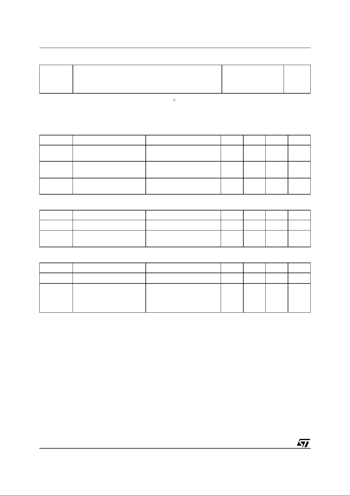
■ DOUBLE DICE IN COMMON DRAIN
CONFIGURATION
DESCRIPTION
This Power MOSFET is the latest dev elo pment of
STMicroelectronis unique "Single Feature Size™"
strip-based process. The resulting transistor
shows extremely high packing density for low onresistance.
APPLICATIONS
■ DC MOTOR DRIVE
■ DC-DC CONVERTERS
■ BATTERY SAFETY UNIT FOR NOMADIC
EQUIPMENT
■ POWER MANAGEMENT IN
PORTABLE/DESKTOP PCs
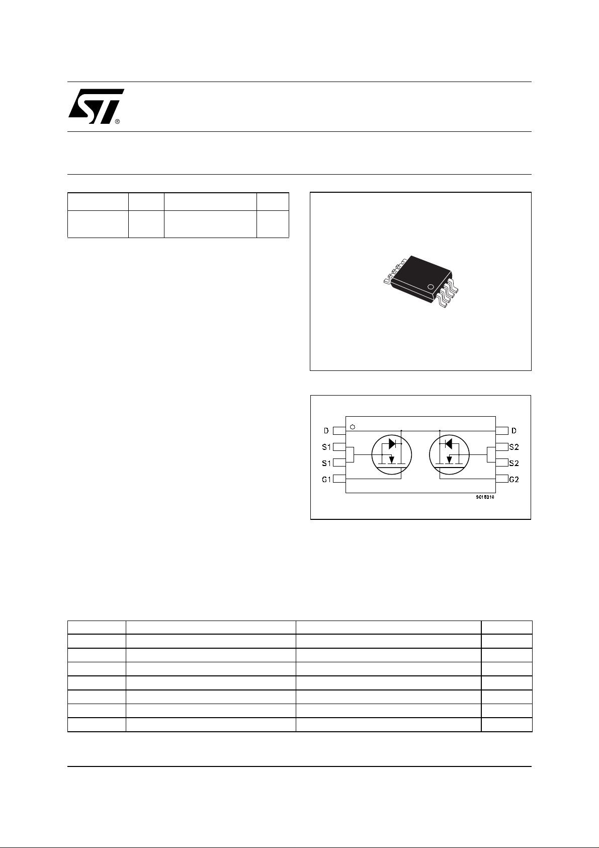
TSSOP8
INTERNAL SCHEMATIC DIAGRAM
ABSOLUTE MAXIMUM RATINGS
Symbol Parameter Value Unit
V
DS
V
DGR
V
GS
I
D
I
D
(
I
DM
P
tot
(
Pulse widt h l i m i ted by safe operating area.
•)
Drain-source Voltage (VGS = 0)
Drain-gate Voltage (RGS = 20 kΩ)
30 V
30 V
Gate- source Voltage ± 12 V
Drain Current (continuous) at TC = 25°C
Drain Current (continuous) at TC = 100°C
•)
Drain Current (pulsed) 24 A
Total Dissipation at TC = 25°C
6A
3.8 A
1.5 W
1/8February 2003
Page 2
STC6NF30V
THERMA L D ATA
Rthj-pcb
Rthj-pcb
T
T
stg
Thermal Resistance Junction-PCB (**)
Thermal Resistance Junction-PCB (*)
Operating Junction Temperature
j
Storage temperature
Max
Max
100
83.5
-55 to 150
-55 to 150
°C/W
°C/W
°C
°C
(*) When Mounted on FR- 4 board with 1 inch
2
pad, 2 oz of Cu a nd t [ 10 sec
(**) When Mounted on minimum recom mended foot print
ELECTRICAL CHARACTERISTICS (Tj = 25 °C unless otherwise specified)
OFF
Symbol Parameter Test Conditions Min. Typ. Max. Unit
V
(BR)DSS
Drain-source
I
= 250 µA, VGS = 0
D
30
Breakdown Voltage
V
= Max Rating
DS
V
= Max Rating TC = 125°C
DS
= ± 12 V
V
GS
1
10
±100 nA
ON
(*)
I
DSS
I
GSS
Zero Gate Voltage
Drain Current (V
GS
Gate-body Leakage
Current (V
DS
= 0)
= 0)
Symbol Parameter Test Conditions Min. Typ. Max. Unit
V
V
GS(th)
R
DS(on)
Gate Threshold Voltage
Static Drain-source On
Resistance
= VGS ID = 250 µA
DS
= 4.5 V ID = 3 A
V
GS
V
= 2.5 V ID = 3 A
GS
0.6 V
0.020
0.025
0.025
0.030
DYNAMIC
Symbol Parameter Test Conditions Min. Typ. Max. Unit
(*)
g
fs
C
iss
C
oss
C
rss
Forward Transconductance
Input Capacitance
Output Capacitance
Reverse Transfer
Capacitance
V
= 10 V ID=6 A
DS
= 25V f = 1 MHz, VGS = 0
V
DS
18 S
800
180
32
V
µA
µA
Ω
Ω
pF
pF
pF
2/8
Page 3

STC6NF30V
ELECTRICAL CHARACTERISTICS (continued)
SWITCHING ON
Symbol Parameter Test Conditions Min. Typ. Max. Unit
t
d(on)
Q
Q
Q
t
r
g
gs
gd
Turn-on Delay Time
Rise Time
Total Gate Charge
Gate-Source Charge
Gate-Drain Charge
SWITCHING OFF
Symbol Parameter Test Conditions Min. Typ. Max. Unit
t
d(off)
t
f
Turn-off Delay Time
Fall Time
SOURCE DRAIN DIODE
Symbol Parameter Test Conditions Min. Typ. Max. Unit
I
SD
I
SDM
V
SD
t
rr
Q
rr
I
RRM
(*)
Pulsed: P ul se duration = 300 µs, duty cycle 1.5 %.
(
•)Pulse width limited by saf e operating area.
Source-drain Current
(•)
Source-drain Current (pulsed)
(*)
Forward On Voltage
Reverse Recovery Time
Reverse Recovery Charge
Reverse Recovery Current
= 15 V ID = 3 A
V
DD
R
= 4.7 Ω VGS = 2.5 V
G
(Resistive Load, Figure 1)
= 15V ID= 6A VGS=2.5V
V
DD
(see test circuit, Figure 2)
= 15 V ID = 3 A
V
DD
R
= 4.7Ω, V
G
GS
= 2.5 V
(Resistive Load, Figure 1)
I
= 6 A VGS = 0
SD
= 6 A di/dt = 100A/µs
I
SD
V
= 15 V Tj = 150°C
DD
(see test circuit, Figure 3)
20
25
6.8
2.0
3.4
32
13
25
21
1.7
9nC
6
24
1.2 V
ns
ns
nC
nC
ns
ns
A
A
ns
nC
A
Safe Operating Area.
Thermal Impedance.
3/8
Page 4

STC6NF30V
Output Characteristics Transfer Characteristics
Transconductance Static Drain-source On Resistance
Gate Charge vs Gate-source Voltage Capacitance Variations
4/8
Page 5

STC6NF30V
Normalized Gate Threshold Voltage vs Temperature Normalized on Resistance vs Temperature
Source-drain Diode Forward Characteristics Normalized Breakdown Voltage Temperature
Thermal resistance and max power
5/8
Page 6

STC6NF30V
Fig. 1: Switching Times Test Circuits For Resistive
Load
Fig. 3: Test Circuit For Diode Recovery Behaviour
Fig. 2: Gate Charge test Circuit
6/8
Page 7

TSSOP8 MECHANICAL DATA
STC6NF30V
DIM.
MIN. TYP. MAX. MIN. TYP. MAX.
mm. inch.
A 1.05 1.20 0.041 0.047
A1 0.05 0.15 0.002 0.006
A2 0.80 1.05 0.032 0.041
b 0.19 0.30 0.008 0.012
c 0.090 0.20 0.003 0.007
D 2.90 3.10 0.114 0.122
E 6.20 6.60 0.240 0.260
E1 4.30 4.50 0.170 0.177
e 0.65 0.025
L 0.45 0.75 0.018 0.030
L1 1.00 0.039
k
o
0
o
8
0.192 0.208
7/8
Page 8

STC6NF30V
Information furnished is believed to be accurate and reliable. However, STMicroelectronics assumes no responsibility for the consequences
of use of such information nor for any infringement of patents or other rights of third parties which may result from its use. No license is granted
by implic ation or oth erwise unde r any paten t or patent ri ght s of STMicroelectronics. Spec i fications me ntioned in this publication are subject
to change without notice. This publication supersedes and replaces all information previously supplied. STMicroelectronics product s are not
authorized for use as critical components in life su pport devices or systems wit hout express written appr oval of STMicroelectronics.
The ST logo is registered trademark of STMicroelectronics
2002 STMi croelectronics - All Rights Reserv ed
All other na m es are the property of their res pective owners.
Australi a - Brazil - Canada - China - Fi nl and - France - Germany - Hong Kong - India - Is rael - Italy - Ja pan - Malaysi a - Malta - Morocco -
Singap ore - Spain - Sw eden - Switzerl and - United K i ngdom - United States.
STMicroelectronics GROUP OF COMPANIES
http:// www.st.com
8/8
 Loading...