

Page 1
®
HIGH VOLTAGE FAST-SWITCHING
■ MEDIUM V O LTA GE C A PA B ILI TY
■ LOW SPREAD OF DYNAMIC PARAMETERS
■ MINIMUM LOT-TO-LO T SPREAD FOR
RELIAB LE OP ERA T ION
■ VERY HIGH SWITCHING SPEED
APPLICATIONS:
■ ELECTRONIC BA LLAS TS FOR
FLUORESCE NT LIG HT I NG
DESCRIPTION
The device is manufactured using high voltage
Multi Epitaxial Planar technology for high
switching speeds and medium voltage capabilit y.
It uses a Cellular Emitter structure with planar
edge termination to enhance switching speeds
while maintaining the wide RBSOA.
The STBV68 is designed for use in compact
fluorescent lamp application.
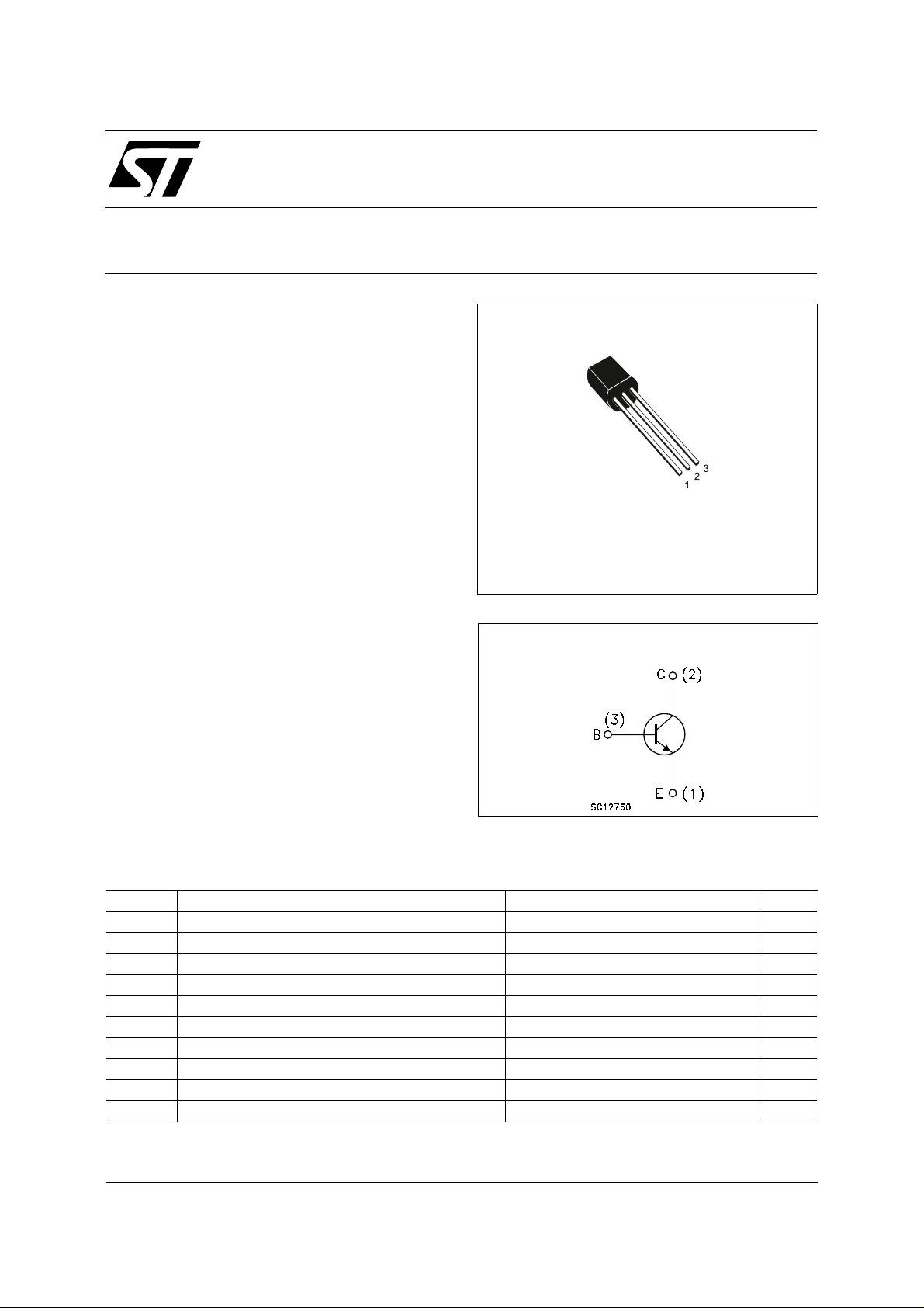
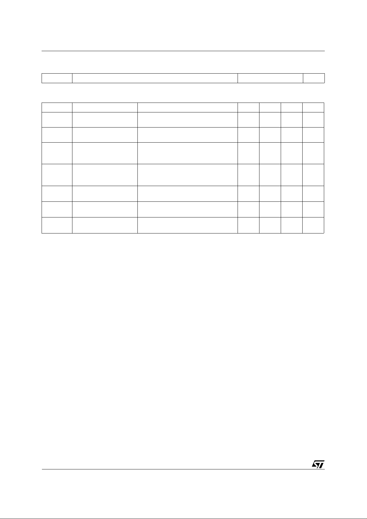
STBV68
NPN POWER TRANSISTOR
TO-92
INTERNAL SCHEMAT I C DIAGRAM
ABSOLUTE MA XIMU M RAT INGS
Symbol Parameter Value Unit
V
V
V
I
I
P
T
September 2000
Collector-Emitter Voltage (VBE = 0) 600 V
CES
Collector-Emitter Voltage (IB = 0) 400 V
CEO
Emitter-Base Voltage (IC = 0) 9 V
EBO
Collector Current 0.6 A
I
C
Collector Peak Current (tp < 5 ms) 1.2 A
CM
Base Current 0.3 A
I
B
Base Peak Current (tp < 5 ms) 0.6 A
BM
Total Dissipation at T
tot
Storage Temperature -65 to 150
stg
Max. Operating Junction Temperature 150
T
j
= 25 oC 0.9 W
amb
o
C
o
C
1/4
Page 2
STBV68
THERMAL DATA
R
thj-amb
Thermal Resistance Junction-ambient Max 140
o
C/W
ELECTRICAL CHARACTERISTICS (T
= 25 oC unless otherwise specif ied)
case
Symbol Parameter Test Conditions Min. Typ. Max. Unit
I
CEV
I
EBO
V
CEO(sus)
Collector Cut-off
Current (V
= -1.5 V)
BE
Emitter Cut-off Current
(I
= 0)
C
∗ Collector-Emitter
= 600 V 250 µA
V
CE
= 9 V 1 mA
V
BE
I
= 1 mA L = 25mH 400 V
C
Sustaining Voltage
(I
= 0)
B
V
CE(sat)
V
BE(sat)
∗ Collector-Emitter
Saturation Voltage
∗ Base-Emitter
Saturation Voltage
IC = 0.1 A IB = 20 mA
I
= 0.15 A IB = 50 mA
C
I
= 0.25 A IB = 100 mA
C
IC = 0.1 A IB = 20 mA
I
= 0.15 A IB = 50 mA
C
hFE∗ DC Current Gain IC = 0.1 A V
I
= 0.25 A V
C
INDUCTIVE LOAD
t
Fall Time
f
∗ Pulsed: Pulse duration = 300µs, duty cycle = 1.5 %
IC = 0.1 A V
I
= - IB2 = 20 mA L =3 mH 0.3 µs
B1
= 5 V
CE
= 10 V
CE
clamp
0.35
0.8
3.0
7
3
= 300 V
0.75
1.5
5
1.0
1.2
15
6
V
V
V
V
V
2/4
Page 3

TO-92 MECHANICAL DATA
STBV68
DIM.
MIN. TYP. MAX. MIN. TYP. MAX.
A 4.58 5.33 0.180 0.210
B 4.45 5.2 0.175 0.204
C 3.2 4.2 0.126 0.165
D 12.7 0.500
E1.27 0.050
F 0.4 0.51 0.016 0.020
G0.35 0.14
mm inch
3/4
Page 4

STBV68
Information furnished is believed to be accurate and reliable. However, STMicroelectronics assumes no responsibility for the consequences
of use of such inform ation nor for any infringe ment o f patents or other rig hts o f third par ties which ma y resul t from i ts use. N o li cen se is
granted by implicatio n or otherwise under any patent or patent rights of STMicroelectronics. Specification mentioned in this publication are
subject to change without notice. This publication supersedes and replaces all information previously supplied. STMicroelectronics products
are not authorized for use as critical compo nents in life support devices or systems without express written approval of STMicroelectronics.
The ST logo is a trademark of STMicroelectronics
© 2000 STMicroelectro nics – Printed in Italy – All Rights Reserved
STMicroelectronics GROUP OF COMPANIES
Australia - Brazil - China - Finland - France - Germany - Hong Kong - India - Italy - Japan - Malaysia - Malta - Morocco -
Singapore - Spain - Sweden - Switzerland - United Kingdom - U.S.A.
http://www.st.com
4/4
 Loading...