

Page 1
HIGH VOLTAGE FAST-SWITCHING
■ ST13003SILICONIN TO-92 PACKAGE
■ MEDIUMVOLTAGECAPABILITY
■ LOW SPREADOF DYNAMICPARAMETERS
■ MINIMUMLOT-TO-LOT SPREAD FOR
RELIABLEOPERATION
■ VERYHIGH SWITCHING SPEED
APPLICATIONS:
■ ELECTRONICBALLASTSFOR
FLUORESCENT LIGHTING
STBV32
NPN POWER TRANSISTOR
DESCRIPTION
The device is manufactured using high voltage
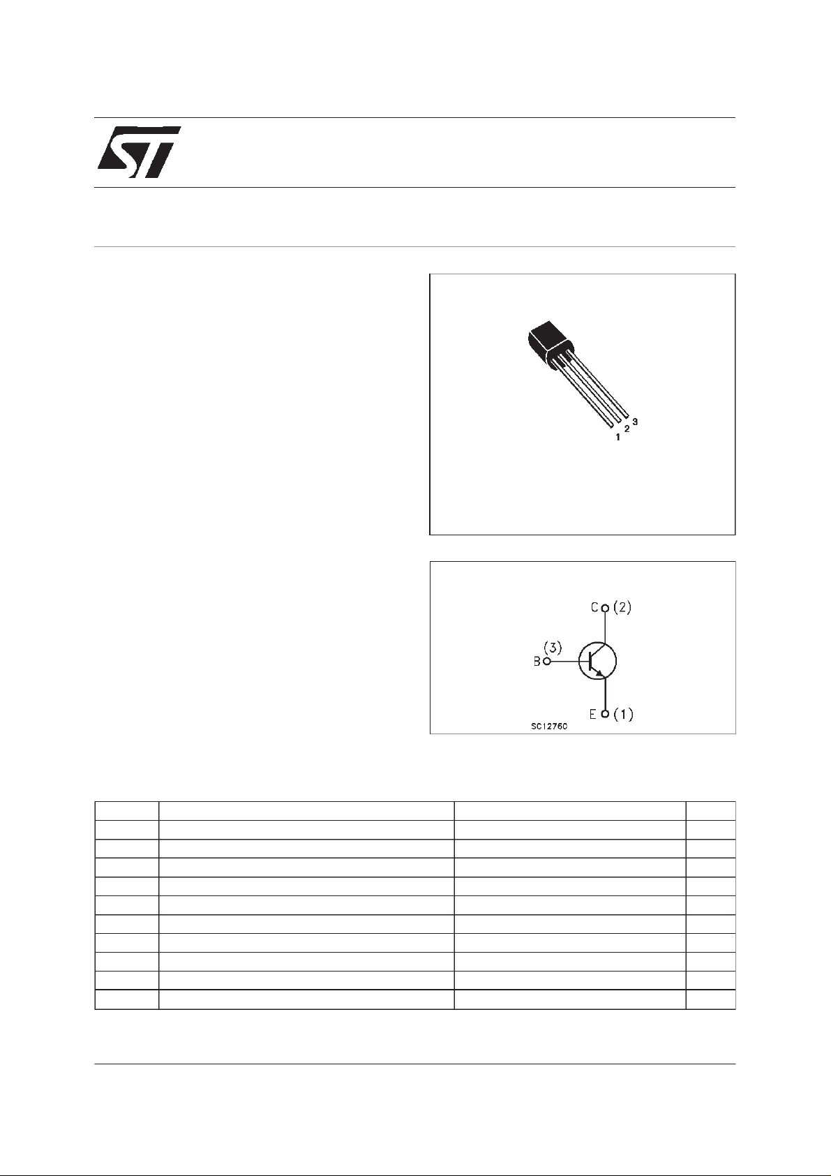
TO-92
Multi Epitaxial Planar technology for high
switchingspeeds andmedium voltage capability.
It uses a Cellular Emitter structure with planar
edge termination to enhance switching speeds
while maintainingthe wide RBSOA.
The STBV32 is designed for use in compact
INTERNAL SCHEMATIC DIAGRAM
fluorescentlamp application.
ABSOLUTE MAXIMUM RATINGS
Symbol Parameter Value Unit
V
V
V
I
I
P
T
Collect or-Emit t e r Voltage ( VBE= 0) 700 V
CES
Collect or-Emit t e r Voltage ( IB= 0) 400 V
CEO
Emitter-Base Vol tage (IC=0) 9 V
EBO
Collect or Current 1.5 A
I
C
Collect or Peak Cu r rent (tp<5ms) 3 A
CM
Base Cu rr ent 0.75 A
I
B
Base P eak Cu rrent (tp<5ms) 1.5 A
BM
Tot al Dissipation at Tc=25oC1.1W
tot
Storage Temperature -65 to 150
stg
Max. Ope r ating Junc t io n Tempe rature 150
T
j
o
C
o
C
February 2000
1/7
Page 2

STBV32
THERMAL DATA
R
thj-case
Ther mal Resist an c e Junct io n-c a s e Max 112
o
C/W
ELECTRICAL CHARACTERISTICS (T
=25oC unlessotherwise specified)
case
Symbol Parameter Test Cond itions Min. Typ. Max. Un it
I
CEV
I
EBO
V
CEO(sus)
V
CE(sat)
V
BE(sat)
h
FE
Collec t or Cut -off
Current (V
=-1.5V)
BE
Emitter Cut-off
Current (I
C
=0)
∗ Co llector-E m itter
Sust aining Voltage
=0)
(I
B
∗ Collector-E mitter
Saturation Voltage
∗ Base-Emitt er
Saturation Voltage
= 700V
V
CE
V
= 700V Tj= 125oC
CE
V
=9V 1 mA
EB
I
=10mA
C
L=25mH
IC=0.5A IB=0.1A
=1A IB=0.25A
I
C
=1.5A IB=0.5A
I
C
IC=0.5A IB=0.1A
=1A IB=0.25A
I
C
∗ DC C ur rent Gain IC=0.5A VCE=2V
I
=1A VCE=2V
C
1
5
400 V
0.5
1
3
1.0
1.2
8
5
35
25
RESI STIVE LOAD
t
Rise T ime
r
t
s
t
f
Storage Ti me
Fall Time
INDUCTIV E LOAD
t
∗
Pulsed: Pulse duration = 300µs, duty cycle = 1.5 %.
s
Storage Ti me
=1A VCC=125V
I
C
=0.2A IB2=-0.2A
I
B1
=25µs
T
p
IC=1A IB1=0.2A
=-5V L=50mH
V
BE
=300V
V
clamp
0.8 µs
1.0
4.0
0.7
mA
mA
V
V
V
V
V
µs
µs
µs
2/7
Page 3

STBV32
Safe Operating Area
DCCurrent Gain
DeratingCurve
DC Current Gain
CollectorEmitterSaturationVoltage
BaseEmitter Saturation Voltage
3/7
Page 4

STBV32
InductiveFall Time InductiveStorage Time
ReverseBiased SOA
4/7
Page 5

Figure1: Inductive Load Switching TestCircuits.
Figure2: ResistiveLoad Switching Test Circuits.
STBV32
5/7
Page 6

STBV32
DIM.
A 4.58 5.33 0.180 0.210
B 4.45 5.2 0.175 0.204
C 3.2 4.2 0.126 0.165
D 12.7 0.500
E 1.27 0.050
TO-92 MECHANICAL DATA
mm inch
MIN. TYP. MAX. MIN. TYP. MAX.
F 0.4 0.51 0.016 0.020
G 0.35 0.14
6/7
Page 7

STBV32
Information furnished is believed tobe accurate and reliable. However, STMicroelectronics assumes no responsibility for the consequences
of use of such information nor for any infringement of patents or other rights of third parties which may result from its use. No license is
granted by implication or otherwise under any patent or patent rights of STMicroelectronics. Specification mentioned in this publication are
subject to change without notice. This publication supersedes and replaces all information previously supplied. STMicroelectronics products
are not authorized for use as critical components in life support devices or systems without express written approval of STMicroelectronics.
The ST logo is a trademark of STMicroelectronics
2000 STMicroelectronics – Printed in Italy – All Rights Reserved
STMicroelectronicsGROUP OF COMPANIES
Australia - Brazil - China - Finland - France - Germany - Hong Kong - India - Italy- Japan - Malaysia - Malta - Morocco -
Singapore- Spain - Sweden - Switzerland -United Kingdom - U.S.A.
http://www.st.com
7/7
 Loading...