

Page 1

STB9NC60
N - CHANNEL 600V - 0.5Ω -9A D2PAK/I2PAK
PowerMESHII MOSFET
TYPE V
DSS
R
DS(on)
I
D
STB9NC60 600 V < 0 .75 Ω 9.0 A
ν TYPICAL R
ν EXTREMELY HIGH dv/dt CAPABILITY
ν 100% AVALANCHE TESTED
ν NEW HIGH VOLTAGE BENCHMARK
ν GATE CHARGE MINIMIZED
DS(on)
= 0.5 Ω
3
3
2
1
1
DESCRIPTION
The PowerMESHII is the evolution of the first
generation of MESH OVERLAY. The layout
refinements introduced greatly improve the
Ron*area figure of merit while keeping the device
I2PAK
TO-262
(Suffix ”-1”)
D2PAK
TO-263
(Suffix ”T4”)
at the leading edge for what concerns switching
speed, gate charge and ruggedness.
APPLICATIONS
ν HIGH CURRENT, HIGH SPEED SWITCHING
ν SWITH MODE POWER SUPPLIES(SMPS)
ν DC-AC CONVERTERS FOR WELDING
INTERNAL SCHEMATIC DIAGRAM
EQUIPMENT AND UNINTERRUPTIBLE
POWER SUPPLIESAND MOTOR DRIVER
ABSOLUTE MAXIMUM RATINGS
Symbol Parameter Value Unit
V
Drain-source Voltage (VGS=0) 600 V
DS
V
Drain- gate Voltage (RGS=20kΩ)
DGR
Gate-source Voltage ± 30 V
V
GS
I
Drain Current (continuous) at Tc=25oC9.0A
D
I
Drain Current (continuous) at Tc= 100oC5.7A
D
I
(•) Drain Current (pulsed) 36 A
DM
P
Total Dissipation at Tc=25oC125W
tot
Derating Factor 1.0 W/oC
dv/dt(
1) Pe ak Diode Recovery voltage slope 4.5 V/ns
T
Storage Temperature -65 to 150
stg
T
Max. Operating JunctionTemperature 150
j
(•) Pulsewidth limited by safeoperating area (1)ISD≤ 9A, di/dt ≤ 200A/µs, VDD≤ V
600 V
,Tj≤T
(BR)DSS
JMAX
o
C
o
C
January2000
1/9
Page 2
STB9NC60
THERMAL DATA
R
R
R
AVALANCHE CHARACTERISTICS
Symbol Parameter Max Value Unit
Thermal R esistance Junction-case Max 1.0
thj-case
Thermal Resistance Junction-ambient Max
thj-amb
Thermal Resistance Case-sink Typ
thc-sink
Maximum Lead Temperature For Soldering Purpose
T
l
I
AvalancheCurrent, Repetitive or Not-Repetitive
AR
(pulse width limited by T
Single Pulse Avalanche En ergy
E
AS
(startin g T
=25oC, ID=IAR,VDD=50V)
j
max)
j
62.5
0.5
300
9A
850 mJ
o
o
o
C/W
C/W
C/W
o
C
ELECTRICAL CHARACTERISTICS (T
=25oC unless otherwise specified)
case
OFF
Symbol Parameter Test Conditions Min. Typ. Max. Unit
V
(BR)DSS
I
DSS
I
GSS
Drain-source
Breakdown Voltage
Zero Gate Vo ltage
Drain Current (V
GS
Gate-body Leakage
Current (V
DS
=0)
= 250 µAVGS=0
I
D
V
DS
V
=0)
DS
V
GS
=MaxRating
= Max Rating Tc=125oC
= ± 30 V ± 100 nA
600 V
150µA
ON (∗)
Symbol Parameter Test Conditions Min. Typ. Max. Unit
V
GS(th)
R
DS(on)
I
D(on)
Gate ThresholdVoltage
Static Drain-source On
V
DS=VGSID
VGS= 10V ID= 4.5 A 0.6 0.75 Ω
Resistance
On State Drai n Current VDS>I
VGS=10V
= 250 µA
D(on)xRDS(on)max
234V
9.0 A
DYNAMIC
Symbol Parameter Test Conditions Min. Typ. Max. Unit
(∗)Forward
g
fs
Transconductance
C
Input Capacitance
iss
Output Capacitance
C
oss
Reve rse Tra n s fe r
C
rss
Capacitance
VDS>I
D(on)xRDS(on)maxID
=4.5A 10 S
VDS=25V f=1MHz VGS= 0 1400
196
31
µA
pF
pF
pF
2/9
Page 3
STB9NC60
ELECTRICAL CHARACTERISTICS (continued)
SWITCHING ON
Symbol Parameter Test Conditions Min. Typ. Max. Unit
Turn -on D elay Time
t
d(on)
t
Rise Time
r
Q
Total Gate Charge
g
Gate-Source Charge
Q
gs
Gate-D rain Charge
Q
gd
VDD=300V ID=4.5A
R
=4.7 Ω VGS=10V
G
(Resistive Load, see fig. 3)
VDD= 480 V ID=9.0A VGS=10V 55
SWITCHING OFF
Symbol Parameter Test Conditions Min. Typ. Max. Unit
t
d(off)
t
t
r(Voff)
t
t
Turn -of f D e la y T ime
Fall Time
f
Off-voltage Rise Time
Fall Time
f
Cross-over Time
c
VDD=300V ID=4.5A
R
=4.7 Ω VGS=10V
G
(Resistive Load, see fig. 3)
VDD=480V ID=9.0A
=4.7 Ω VGS=10V
R
G
(Inductive Load, see fig. 5)
SOURCE DRAIN DIODE
Symbol Parameter Test Conditions Min. Typ. Max. Unit
Source-drain Current
I
SD
I
(•)
SDM
V
Source-drain Current
(pulsed)
(∗)ForwardOnVoltage ISD=9A VGS=0 1.6 V
SD
t
Reverse R ecovery
I
rr
Q
RRM
rr
Time
Reverse R ecovery
Charge
Reverse R ecovery
Current
= 9 A di/dt = 100 A/µs
I
SD
= 100 V Tj= 150oC
V
DD
(see test circuit, fig. 5)
20
16
77 nC
4.5
31
64
32
19
13
32
9.036A
600
4.7
15.5
ns
ns
nC
nC
ns
ns
ns
ns
ns
A
ns
µC
A
(∗) Pulsed: Pulse duration= 300µs, duty cycle1.5 %
(•) Pulsewidth limited by safeoperating area
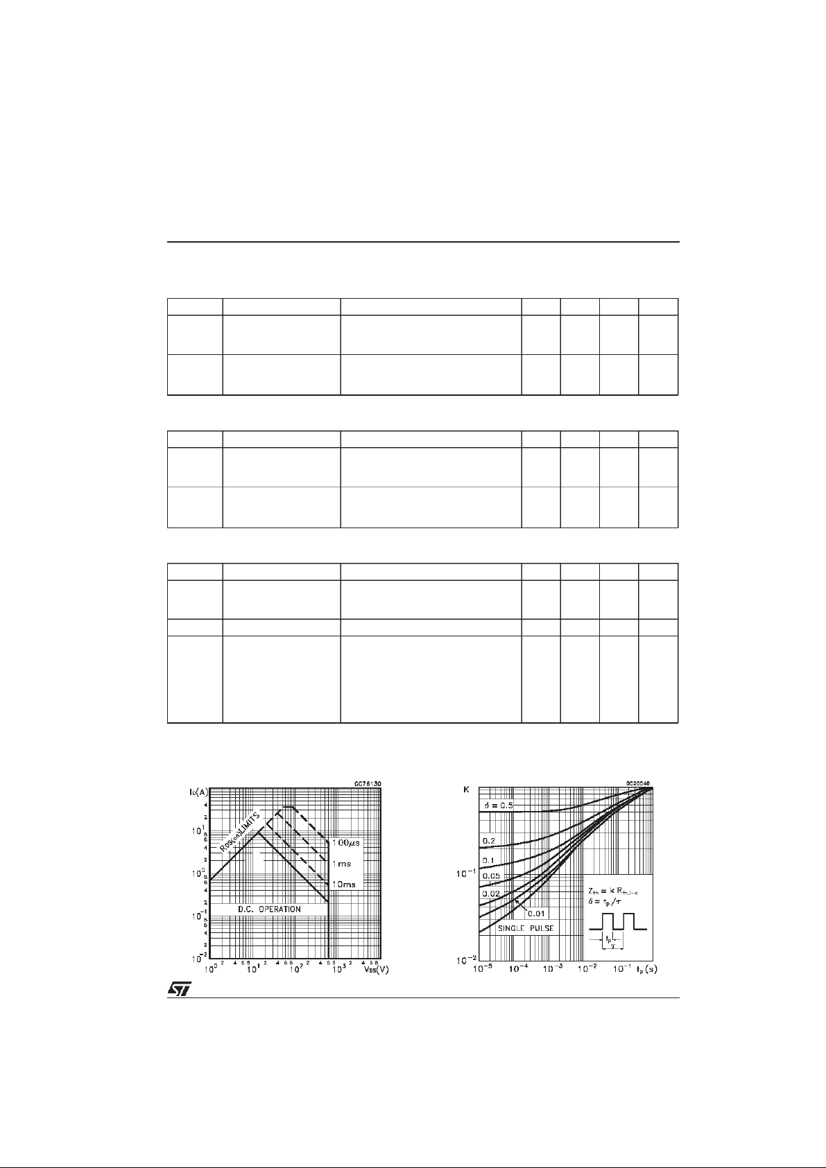
Safe Operating Area ThermalImpedance
3/9
Page 4

STB9NC60
Output Characteristics
Transconductance
Transfer Characteristics
StaticDrain-source On Resistance
Gate Charge vsGate-source Voltage
4/9
CapacitanceVariations
Page 5

STB9NC60
Normalized Gate Threshold Voltage vs
Temperature
Source-drain Diode Forward Characteristics
NormalizedOn Resistance vs Temperature
5/9
Page 6

STB9NC60
Fig. 1: Unclamped Inductive Load Test Circuit
Fig. 3: Switching TimesTest Circuits For
ResistiveLoad
Fig. 2: Unclamped Inductive Waveform
Fig.4: Gate Charge test Circuit
Fig. 5: TestCircuitFor Inductive Load Switching
And Diode RecoveryTimes
6/9
Page 7

TO-262 (I2PAK) MECHANICAL DATA
STB9NC60
DIM.
MIN. TYP. MAX. MIN. TYP. MAX.
A 4.3 4.6 0.169 0.1 81
A1 2.49 2.69 0. 098 0.106
B 0.7 0.93 0.027 0.036
B1 1.2 1.38 0.047 0.0 54
B2 1.25 1.4 0.049 0.055
C 0.45 0.6 0.017 0.0 23
C2 1. 21 1.36 0.047 0.053
D 8.95 9.35 0.352 0.368
e 2.44 2.64 0.096 0.104
E 10 10.28 0.393 0.404
L 13.2 13.5 0.519 0.531
L1 3. 48 3.78 0.137 0.149
L2 1. 27 1.4 0.050 0.055
mm inch
CA1
A
C2
B2
B
e
E
L1
L2
D
L
P011P5/C
7/9
Page 8

STB9NC60
TO-263 (D2PAK) MECHANICALDATA
DIM.
MIN. TYP. MAX. MIN. TYP. MAX.
A 4.3 4.6 0.169 0.1 81
A1 2.49 2.69 0. 098 0.106
B 0.7 0.93 0.027 0.036
B2 1.25 1.4 0.049 0.055
C 0.45 0.6 0.017 0.0 23
C2 1. 21 1.36 0.047 0.053
D 8.95 9.35 0.352 0.368
E 10 10.28 0.393 0.404
G 4.88 5.28 0.192 0.208
L 15 15.8 5 0.590 0.624
L2 1. 27 1.4 0.050 0.055
L3 1.4 1.75 0.055 0.068
mm inch
E
A
C2
L2
8/9
L
D
L3
B2
B
A1
C
G
P011P6/C
Page 9

STB9NC60
Informationfurnished is believe dto beaccurate andrelia ble. However,STMicroelectronicsassumes no responsibilityfor theconseque nces
of use of such informationnor for any infringementof patentsor other rights of third parties which may result from its use. No license is
granted by implication or othe rwiseunder any patentor patent rights of STMicroele ctronics. Specificationmentioned in this publicationare
subject to change withoutnotice.This publicationsupersedesand replacesall information prev iousl ysupplied.STMicroelectr onicsproduct s
are not authorizedfor use as criticalcomponents in life suppor tdevices or syste mswithout express writtenapprova lof STMicroele ctronics.
Australia - Brazil- China - Finland - France - Germany - Hong Kong - India - Italy - Japan- Malaysia - Malta - Morocco -
The ST logo isa trademark of STMicroelectronics
1999STMicroelectronics – Printed in Italy – All RightsReserved
STMicroelectronics GROUP OF COMPANIES
Singapore - Spain - Sweden- Switzerland - United Kingdom - U.S.A.
http://www.st.com
.
9/9
 Loading...