

Page 1
STB9NB50
N - CHANNEL ENHANCEMENT MODE
Power MESH MOSFET
TYPE V
DSS
R
DS(on)
I
D
STB9N B 50 500 V < 0. 8 5 Ω 8.6 A
■ TYPICALR
■ EXTREMELY HIGH dv/dt CAPABILITY
■ AVALANCHERUGGEDTECHNOLOGY
■ 100% AVALANCHETESTED
■ REPETITIVEAVALANCHE DATA AT 100
■ VERYLOW INTRINSIC CAPACITANCE
■ GATECHARGEMINIMIZED
■ LOW LEAKAGE CURRENT
■ APPLICATIONORIENTED
CHARACTERIZATION
■ FORSMD D
=0.75 Ω
DS(on)
2
PAKVERSIONCONTACT
o
C
SALESOFFICE
APPLICATIONS
■ HIGH CURRENT, HIGH SPEEDSWITCHING
■ SWITCHMODEPOWER SUPPLY (SMPS)
■ DC-ACCONVERTER FORWELDING
EQUIPMENTAND UNINTERRUPTABLE
POWERSUPPLY (UPS)
3
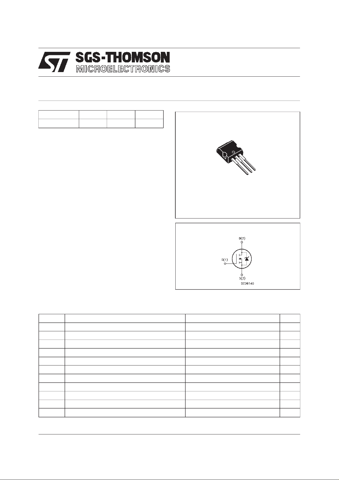
2
1
I2PAK
TO-262
(suffix ”-1”)
INTERNAL SCHEMATIC DIAGRAM
ABSOLUTE MAXIMUM RATINGS
Symbol Parameter Value Unit
V
V
DGR
V
I
DM
P
dv/ dt
T
(•) Pulsewidth limitedby safe operating area (1)ISD≤ 9A, di/dt ≤ 200 A/µs, VDD≤ V
March 1998
Drain-s ou r ce Voltage (VGS= 0) 500 V
DS
Drain- gate Voltage (RGS=20kΩ)
Gate-source Voltage ± 30 V
GS
I
Drain Current (c ontinuous ) at Tc=25oC8.6A
D
I
Drain Current (c ontinuous ) at Tc=100oC5.4A
D
500 V
(•) Drain Current (pulsed) 34.4 A
Tot al Dissipation at Tc=25oC 125 W
tot
Derating Factor 1.0 W/
(1) Peak Diode Recove ry vo lt a ge slope 4.5 V/ns
Storage Temperature -65 to 150
stg
T
Max. Operating J un c t io n Te mperature 150
j
,Tj≤T
(BR)DSS
JMAX
o
C
o
C
o
C
1/8
Page 2
STB9NB50
THERMAL DATA
R
thj-case
R
thj-amb
R
thj-amb
T
AVALANCHE CHARACTERISTICS
Symbol Para met e r Max Va lue Uni t
I
AR
E
Ther mal Resist ance Junction-c a s e Max
Ther mal Resist ance Junction-ambient Max
Ther mal Resist ance Case-sink Ty p
Maximum Lead Temperat ure For Soldering Purpos e
l
Avalanche Curre nt , Rep et itive or Not- Re petitive
(pulse w idth limited by T
Single Pulse Avalanche Energy
AS
(starting T
=25oC, ID=IAR,VDD=50V)
j
max, δ <1%)
j
1
62.5
0.5
300
8.6 A
520 mJ
o
C/W
o
C/W
o
C/W
o
C
ELECTRICAL CHARACTERISTICS (T
=25oC unlessotherwise specified)
case
OFF
Symbol Parameter Test Condition s Min. Typ. Max. Unit
V
(BR)DSS
Drain-source
=250µAV
I
D
GS
=0
500 V
Breakdown Voltage
I
I
DSS
GSS
Zer o Gate V o lt age
Drain Cur re nt (V
GS
Gat e-body Leakage
Current (V
DS
=0)
=0)
=MaxRating
V
DS
V
=MaxRating Tc=125
DS
o
C
= ± 30 V
V
GS
1
50
±100 nA
ON (∗)
Symbol Parameter Test Condition s Min. Typ. Max. Unit
V
GS(th )
Gate Threshold
V
DS=VGSID
=250µA
345V
Voltage
R
DS(on)
Stati c Drain-so urce On
VGS=10V ID= 4.3 A 0.75 0.85 Ω
Resistance
I
D(on)
On S tate Drain Cur rent VDS>I
D(on)xRDS(on)max
8.6 A
VGS=10 V
DYNAMIC
Symbol Parameter Test Condition s Min. Typ. Max. Unit
g
(∗)Forward
fs
Tr ansconductance
C
C
C
Input Capaci t ance
iss
Out put Capa citance
oss
Reverse Transfer
rss
Capa cit an c e
VDS>I
D(on)xRDS(on)maxID
=4.3A 4.5 5.7 S
VDS=25V f=1MHz VGS= 0 1250
175
20
1625
236
27
µA
µA
Ω
pF
pF
pF
2/8
Page 3
STB9NB50
ELECTRICAL CHARACTERISTICS (continued)
SWITCHINGON
Symbol Parameter Test Condition s Min. Typ. Max. Unit
t
d(on)
t
r
Turn-on Time
Rise Tim e
VDD=250V ID=4.3A
=4.7 Ω VGS=10V
R
G
19
11
(see test circuit, figure 3)
Q
Q
Q
Total Gate Charge
g
Gat e-Source Char ge
gs
Gate-Drain Charge
gd
VDD=400V ID=8.6A VGS=10V 32
10.6
13.7
SWITCHINGOFF
Symbol Parameter Test Condition s Min. Typ. Max. Unit
t
r(Voff)
t
t
Of f - voltage Rise T im e
Fall Time
f
Cross-over Time
c
VDD=400V ID=8.6
A
=4.7 Ω VGS=10V
R
G
11.5
11
20
(see test circuit, figure 5)
SOURCE DRAIN DIODE
Symbol Parameter Test Condition s Min. Typ. Max. Unit
I
SD
I
SDM
V
SD
t
Q
I
RRM
(∗) Pulsed: Pulse duration =300 µs, duty cycle 1.5 %
(•) Pulse width limited by safeoperating area
Source-drain Current
(•)
Source-drain Current
(pulsed)
(∗) For ward O n V o lt age ISD=8.6A VGS=0 1.6 V
Reverse Recovery
rr
Time
Reverse Recovery
rr
= 8.6 A di/dt = 100 A/µs
I
SD
=100V Tj=150oC
V
R
(see test circuit, figure 5)
420
3.5
Charge
Reverse Recovery
16.5
Current
30
15
45 nC
17
16
28
8.6
34.4
ns
ns
nC
nC
ns
ns
ns
A
A
ns
µC
A
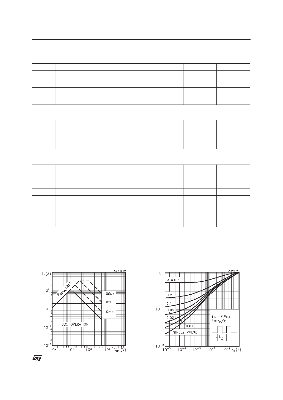
Safe Operating Area ThermalImpedance
3/8
Page 4

STB9NB50
OutputCharacteristics
Transconductance
TransferCharacteristics
StaticDrain-sourceOn Resistance
GateCharge vs Gate-sourceVoltage
4/8
CapacitanceVariations
Page 5

STB9NB50
Normalized Gate Threshold Voltage vs
Temperature
Source-drainDiode Forward Characteristics
Normalized On Resistancevs Temperature
5/8
Page 6

STB9NB50
Fig. 1: Unclamped InductiveLoad Test Circuit
Fig. 3: SwitchingTimes Test CircuitsFor
ResistiveLoad
Fig. 2: Unclamped Inductive Waveform
Fig. 4: Gate Chargetest Circuit
Fig. 5: Test Circuit For InductiveLoad Switching
And Diode RecoveryTimes
6/8
Page 7

TO-262(I2PAK) MECHANICALDATA
STB9NB50
DIM.
MIN. TYP. MAX. MIN. TYP. MAX.
A 4.3 4.6 0.169 0.181
A1 2.49 2.69 0.098 0.106
B 0.7 0.93 0.027 0.036
B1 1.2 1.38 0.047 0.054
B2 1.25 1.4 0.049 0.055
C 0.45 0.6 0.017 0.023
C2 1.21 1.36 0.047 0.053
D 8.95 9.35 0.352 0.368
e 2.44 2.64 0.096 0.104
E 10 10.28 0.393 0.404
L 13.2 13.5 0.519 0.531
L1 3.48 3.78 0.137 0.149
L2 1.27 1.4 0.050 0.055
mm inch
CA1
A
C2
B2
B
e
E
L1
L2
D
L
P011P5/C
7/8
Page 8

STB9NB50
Information furnished is believed to be accurate and reliable. However, SGS-THOMSON Microelectronics assumes no responsability for the
consequences of use of such information nor for anyinfringement of patents or other rightsof third parties which may results from itsuse. No
license is granted by implication or otherwise under any patent orpatentrights of SGS-THOMSON Microelectronics. Specifications mentioned
in thispublication are subject to change without notice. This publication supersedes and replaces all information previously supplied.
SGS-THOMSON Microelectronics products are not authorized for useas criticalcomponentsin life support devices orsystems withoutexpress
written approval ofSGS-THOMSON Microelectonics.
1998 SGS-THOMSON Microelectronics - Printed in Italy - All RightsReserved
Australia - Brazil - Canada -China- France - Germany - Italy - Japan- Korea - Malaysia - Malta - Morocco - The Netherlands-
Singapore - Spain - Sweden - Switzerland - Taiwan - Thailand - United Kingdom - U.S.A
8/8
SGS-THOMSON Microelectronics GROUP OF COMPANIES
...
 Loading...