

Page 1
Philips Semiconductors RF Communications Products Product specification
SA601Low voltage LNA and mixer - 1GHz
1
December 15, 1994 853-1733 14477
DESCRIPTION
The SA601 is a combined RF amplifier and mixer designed for
high-performance low-power communication systems from
800-1200MHz. The low-noise preamplifier has a 1.6dB noise figure
at 900MHz with 11.5dB gain and an IP3 intercept of -2dBm at the
input. The gain is stabilized by on-chip compensation to vary less
than ±0.2dB over -40 to +85°C temperature range. The
wide-dynamic-range mixer has a 9.5dB noise figure and IP3 of
–2dBm at the input at 900MHz. The nominal current drawn from a
single 3V supply is 7.4mA. The Mixer can be powered down to
further reduce the supply current to 4.4mA.
FEATURES
•Low current consumption: 7.4mA nominal, 4.4mA with the mixer
powered-down
•Outstanding LNA noise figure: 1.6dB at 900MHz
•High system power gain: 18dB (LNA + Mixer) at 900MHz
•Excellent gain stability versus temperature and supply voltage
•External >-7dBm LO can be used to drive the mixer
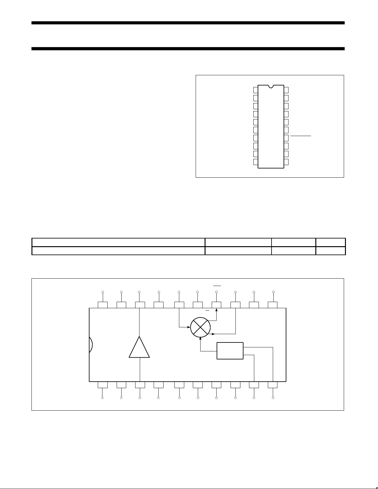
PIN CONFIGURATION
DK Package
1
2
3
4
5
6
7
8
9
10
11
12
13
14
20
19
18
17
16
15
V
CC
GND
LNA OUT
GND
MIXER IN
GND
MIXER OUT
MIXER OUT
GND
V
CC
V
CC
LNA GND
LNA IN
GND
GND
GND
MIXER PWRDN
GND
LOIN1
LOIN2
APPLICATIONS
•900MHz cellular front-end (NADC, GSM, AMPS, TACS)
•900MHz cordless front-end (CT1, CT2)
•900MHz receivers
ORDERING INFORMATION
DESCRIPTION TEMPERATURE RANGE ORDER CODE DWG #
20-Pin Plastic Shrink Small Outline Package (Surface-mount, SSOP)
-40 to +85°C
SA601DK 1563
BLOCK DIAGRAM
4321 5
20 19 18 17 16
76 1098
15 14 13 12 11
GNDMIXER
PWRDN
LO IN1 LO IN2
V
CC
GND
MIXER
IN GND
MIXER
OUT GND
LNA
LO
RF
IF
GND LNA IN GND
IF
GND
LNA
OUT
GNDGND
MIXER
OUT V
CC
V
CC
BUFFER
Page 2
Philips Semiconductors RF Communications Products Product specification
SA601Low voltage LNA and mixer - 1GHz
December 15, 1994
2
ABSOLUTE MAXIMUM RATINGS
3
SYMBOL PARAMETER RATING UNITS
V
CC
Supply voltage
1
-0.3 to +6 V
V
IN
Voltage applied to any other pin -0.3 to (VCC + 0.3) V
P
D
Power dissipation, TA = 25°C (still air)
2
20-Pin Plastic SSOP 980 mW
T
JMAX
Maximum operating junction temperature 150 °C
P
MAX
Maximum power input/output +20 dBm
T
STG
Storage temperature range –65 to +150 °C
NOTE:
1. Transients exceeding 8V on V
CC
pin may damage product.
2. Maximum dissipation is determined by the operating ambient temperature and the thermal resistance,
θ
JA
: 20-Pin SSOP = 110°C/W
3. Pins 9 and 10 are sensitive to electrostatic discharge (ESD).
RECOMMENDED OPERATING CONDITIONS
SYMBOL PARAMETER RATING UNITS
V
CC
Supply voltage 2.7 to 5.5 V
T
A
Operating ambient temperature range -40 to +85 °C
T
J
Operating junction temperature -40 to +105 °C
DC ELECTRICAL CHARACTERISTICS
VCC = +3V, TA = 25°C; unless otherwise stated.
LIMITS
SYMBOL
PARAMETER
TEST CONDITIONS
MIN TYP MAX
UNITS
7.4
ICCSupply current
Mixer power-down input low 4.4
mA
V
LNA–IN
LNA input bias voltage 0.78 V
V
LNA–OUT
LNA output bias voltage 2.1 V
V
MX–IN
Mixer RF input bias voltage 0.94 V
Page 3
Philips Semiconductors RF Communications Products Product specification
SA601Low voltage LNA and mixer - 1GHz
December 15, 1994
3
AC ELECTRICAL CHARACTERISTICS
VCC = +3V, TA = 25°C; LOIN = -7dBm @ 964MHz; unless otherwise stated.
LIMITS
SYMBOL
PARAMETER
TEST CONDITIONS
-3σ TYP +3σ
UNITS
S
21
Amplifier gain 881MHz 10 11.5 13 dB
∆S21/∆T Gain temperature sensitivity 881MHz 0.003 dB/°C
∆S21/∆f Gain frequency variation 800MHz - 1.2GHz 0.01 dB/MHz
S
12
Amplifier reverse isolation 881MHz -20 dB
S
11
Amplifier input match
1
881MHz -10 dB
S
22
Amplifier output match
1
881MHz -10 dB
P
-1dB
Amplifier input 1dB gain compression 881MHz -16 dBm
IP3 Amplifier input third order intercept f
2
– f1 = 25kHz, 881MHz -3.5 -2 -0.5 dBm
NF Amplifier noise figure 881MHz 1.3 1.6 1.9 dB
VG
C
Mixer voltage conversion gain: RP = RL = 1kΩ
fS = 881MHz, fLO = 964MHz,
f
IF
= 83MHz
18.0 19.5 21.0 dB
PG
C
Mixer power conversion gain: RP = RL = 1kΩ
fS = 881MHz, fLO = 964MHz,
f
IF
= 83MHz
5.0 6.5 8.0 dB
S
11M
Mixer input match
1
881MHz -10 dB
NF
M
Mixer SSB noise figure 881MHz 8.0 9.5 11.0 dB
P
-1dB
Mixer input 1dB gain compression 881MHz -13 dBm
IP3
M
Mixer input third order intercept f
2
– f1 = 25kHz, 881MHz -3.5 -2 -0.5 dBm
IP
2INT
Mixer input second order intercept 881MHz 12 dBm
P
RFM-IF
Mixer RF feedthrough 881MHz -7 dB
P
LO-IF
LO feedthrough to IF 881MHz -25 dB
P
LO-RFM
LO to mixer input feedthrough 881MHz -38 dB
P
LO-RF
LO to LNA input feedthrough 881MHz -40 dB
P
LNA–RFM
LNA output to mixer input 881MHz -40 dB
P
RFM–LO
Mixer input to LO feedthrough 881MHz -23 dB
LO
IN
LO drive level 964MHz -7 dBm
NOTE:
1. Simple L/C elements are needed to achieve specified return loss.
Page 4
Philips Semiconductors RF Communications Products Product specification
SA601Low voltage LNA and mixer - 1GHz
December 15, 1994
4
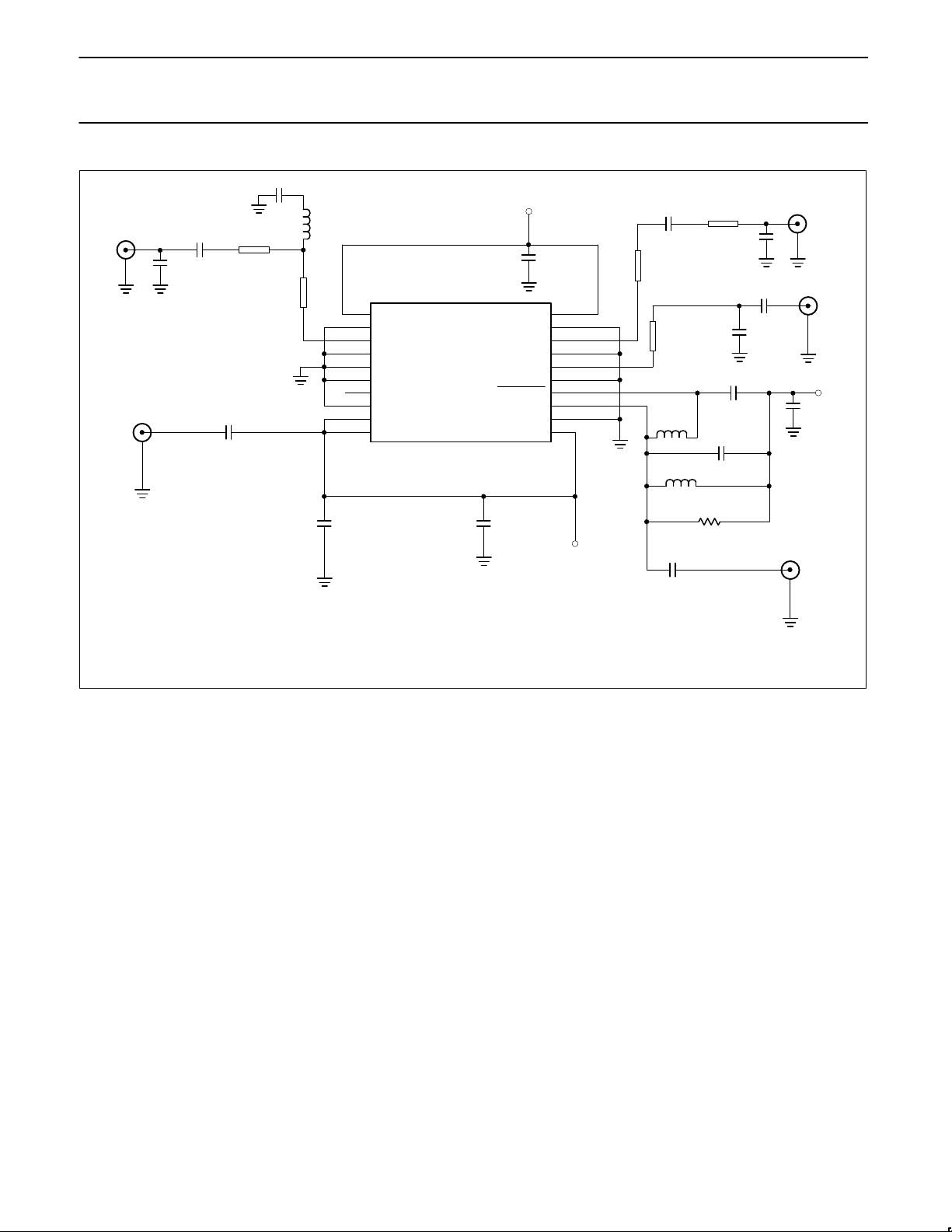
Figure 1. Application Circuit
1
2
3
4
5
6
7
8
9
10
20
19
18
17
16
15
14
13
12
11
Vcc
GND
LNA IN
GND
GND
MIXER PD
GND
LO IN
LO IN
Vcc
GND
LNA OUT
GND
MIXER IN
GND
MIXER OUT
MIXER OUT
GND
GND
Vcc
LNA IN
C1
C15
L1
56nH
C2
2.7pF
100pF
C11
100pF
C12
2.2pF
LNA OUT
C10
100pF
MIXER IN
C9
4.7pF
C13
100pF
270nH
C6
8.2pF
L = 110 mils
L = 95 mils
w = 15 mils
w = 15 mils
V
CC
1µF
100pF
SA601
C4
U1
V
CC
J1
C14
100nF
J2
EXT LO
(-7dBm, 964MHz)
J5
L = 190 mils
w = 15 mils
J4
V
CC
18pF
2.2k
C8
100nF
MIXER OUT
J3
(50Ω, 83MHz)
C3
100pF
33pF
L3
L2
470nH
R2
C5
C7
L = 535 mils
w = 10 mils
L = 535 mils
w = 10 mils
*SEE MIXER POWER GAIN NOTE BELOW
*
**
** SPIRAL INDUCTORS ON NATURAL FR-4, 62 MILS THICK
**
***
***
SEE MIXER FILTER INTERFACE NOTE BELOW
CIRCUIT TECHNOLOGY
LNA
Impedance Match: Intrinsic return loss at the input and output ports
is 7dB and 9dB, respectively. With no external matching, the
associated LNA gain is ≈10dB and the noise figure is ≈1.4dB.
However, the return loss can be improved at 881MHz using
suggested L/C elements (Figure 1) as the LNA is unconditionally
stable.
Noise Match: The LNA achieves 1.6dB noise figure at 881MHz
when S
11
= -10dB. Further improvements in S11 will slightly
decrease the NF and increase S
21
.
Temperature Compensation: The LNA has a built-in temperature
compensation scheme to reduce the gain drift to 0.003dB/°C from
–40°C to +85°C.
Supply Voltage Compensation: Unique circuitry provides gain
stabilization over wide supply voltage range. The gain changes no
more than 0.5dB when V
CC
increases from 3V to 5V.
LO Drive Level: Resistor R1 can be replaced by an inductor of
4.7nH and C13 should be adjusted to achieve a good return loss at
the LO port. Under this condition, the mixer will operate with less
than -10dBm LO drive.
IP3 Performance: C9 between Pin 16 and ground can be removed
to introduce 3dB mismatch loss, while improving the IP3 to +3dBm.
The associated noise figure is 11dB.
Mixer
Input Match: The mixer is configured for maximum gain and best
noise figure. The user needs to supply L/C elements to achieve this
performance.
Power Gain: The gain can be increased by approximately 1.5dB by
placing R2 across C7, instead of C5.
Power Down: The mixer can be disabled by connecting Pin 7 to
ground. When the mixer is disabled, 3mA is saved.
Power Combining: The mixer output circuit features passive
power combining (patent pending) to optimize conversion gain and
noise figure performance without using extra DC current or
degrading the IP3. For IF frequencies significantly different than
83MHz, the component values must be altered accordingly.
Filter Interface: For system integration where a high impedance
filter of 1kΩ is to be cascaded at the mixer IF output, capacitors C5
and C6 need to be changed to 27pF and 1000pF, respectively .
Page 5

Philips Semiconductors RF Communications Products Product specification
SA601Low voltage LNA and mixer - 1GHz
December 15, 1994
5
Figure 2. SA601 Demoboard Layout (Not Actual Size)
Bottom View
Top View
Via Layer
Silk Screen
R1
C11
Page 6

Philips Semiconductors RF Communications Products Product specification
SA601Low voltage LNA and mixer - 1GHz
December 15, 1994
6
TYPICAL PERFORMANCE CHARACTERISTICS
CH1 S
22
1 U FS 4: 99.543 Ω -85.949 Ω 8.937 pF
START 200.000 000 MHz STOP 1200.000 000 MHz
1:
2:
3:
31.48 Ω
-14.217 Ω
900 MHz
44.82 Ω
-30.191 Ω
600 MHz
58.725 Ω
-50.83 Ω
400 MHz
200.000 000 MHz
Figure 3. LNA Input and Output Match (at Device Pin)
CH1 S
11
1 U FS 4: 63.852 Ω -160.23 Ω 4.9269 pF
200.000 000 MHz
START 200.000 000 MHz STOP 1200.000 000 MHz
1:
2:
3:
27.471 Ω
-35.48 Ω
600 MHz
21.286 Ω
-12.381 Ω
900 MHz
36.43 Ω
-70.445 Ω
400 MHz
Page 7

Philips Semiconductors RF Communications Products Product specification
SA601Low voltage LNA and mixer - 1GHz
December 15, 1994
7
TYPICAL PERFORMANCE CHARACTERISTICS (Continued)
CH1
S
12
100mU FS 4: 35.343 mU -76.128 °
200.000 000 MHz
START 200.000 000 MHz STOP 1200.000 000 MHz
1:
2:
3:
89.561mU
61.127 °
900 MHz
74.51mU
64.608 °
600 MHz
58.082mU
67.162 °
400 MHz
CH1
S
21
7 U FS 4: 6.2863 U -150.58 °
200.000 000 MHz
START 200.000 000 MHz STOP 1200.000 000 MHz
1:
2:
3:
3.2504U
91.219 °
900 MHz
4.6877U
112.03 °
600 MHz
5.3895U
130.33 °
400 MHz
Figure 4. LNA Transmission and Isolation Characteristics (at Device Pin)
Page 8

Philips Semiconductors RF Communications Products Product specification
SA601Low voltage LNA and mixer - 1GHz
December 15, 1994
8
TYPICAL PERFORMANCE CHARACTERISTICS (Continued)
CH1
S
11
1 U FS 4: 10.867Ω 1.6426Ω 1.2543 nH
200.000 000 MHz
START 200.000 000 MHz STOP 1200.000 000 MHz
1: 6.7168 Ω
9.5952 Ω
900 MHz
Figure 5. Mixer RF Input Match (at Device Pin)
Table 1. Typical LNA and Mixer S-Parameters
LNA Mixer
f S
11
S
22
S
21
S
12
S
11
200MHz 63.852Ω – j 160.23Ω 99.543Ω – j 85.949Ω 6.2863U ∠ 150.58° 35.343mU ∠ 76.128° 10.867Ω + j 1.6426Ω
300MHz 44.879Ω – j 101.69Ω 73.387Ω – j 67.707Ω 5.8096U ∠ 140.47° 47.946mU ∠ 71.169° 10.4Ω + j 3.4609Ω
400MHz 36.43Ω – j 70.445Ω 58.725Ω – j 50.83Ω 5.3895U ∠ 130.33° 58.082mU ∠ 67.162° 10.067Ω + j 4.897Ω
500MHz 30.395Ω – j 48.393Ω 49.928Ω – j 38.813Ω 5.0428U ∠ 120.5° 66.44mU ∠ 66.388° 9.394Ω + j 6.0142Ω
600MHz 27.471Ω – j 35.48Ω 44.82Ω – j 30.191Ω 4.6877U ∠ 112.03° 74.51mU ∠ 64.608° 8.8945Ω + j 7.2227Ω
700MHz 24.428Ω – j 25Ω 39.268Ω – j 24.502Ω 4.2409U ∠ 104.44° 82.235mU ∠ 65.002° 8.1353Ω + j 8.1597Ω
800MHz 22.434Ω – j 17.255Ω 34.664Ω – j 18.59Ω 3.7491U ∠ 97.765° 86.582mU ∠ 62.743° 7.976Ω + j 9.1958Ω
900MHz 21.286Ω – j 12.381Ω 31.48Ω – j 14.217Ω 3.2504U ∠ 91.219° 89.561mU ∠ 61.127° 6.7168Ω + j 9.5952Ω
1000MHz 20.261Ω – j 8.7109Ω 27.887Ω – j 10.77Ω 2.8785U ∠ 84.957° 95.135mU ∠ 60.539° 6.2393Ω + j 10.271Ω
1100MHz 19.718Ω – j 6.252Ω 25.741Ω – j 8.2607Ω 2.5752U ∠ 82.893° 97.348mU ∠ 62.202° 6.0791Ω + j 10.571Ω
1200MHz 19.101Ω – j 4.9316Ω 23.584Ω – j 6.2715Ω 2.1386U ∠ 80.257° 96.558mU ∠ 61.563° 5.8185Ω + j 10.288Ω
Page 9

Philips Semiconductors RF Communications Products Product specification
SA601Low voltage LNA and mixer - 1GHz
December 15, 1994
9
TYPICAL PERFORMANCE CHARACTERISTICS (Continued)
CH1 S
11 log MAG 2 dB/ REF -5 dB
-40°C
85°C
25°C
START 800.000 000 MHz STOP 1 200. 000 000 MHz
Mixer RF Input Match vs. Frequency
(V
CC
= 3V)
CH1 S
12 log MAG 5 dB/ REF -10 dB
START 800.000 000 MHz STOP 1 200. 000 000 MHz
CH1 S
21 log MAG 1 dB/ REF 10 dB
START 800.000 000 MHz STOP 1 200. 000 000 MHz
CH1 S
22 log MAG 3 dB/ REF -10 dB
START 800.000 000 MHz STOP 1 200. 000 000 MHz
CH1 S
11 log MAG 1 dB/ REF -10 dB
START 800.000 000 MHz STOP 1 200. 000 000 MHz
-40°C
85°C
25°C
LNA Gain (S21) vs. Frequency
(V
CC
= 3V)
-40°C
85°C
25°C
-40°C
85°C
25°C
-40°C
85°C
25°C
LNA Isolation (S12) vs. Frequency
(V
CC
= 3V)
LNA Input Match (S
11
) vs. Frequency
(V
CC
= 3V)
LNA Output Match (S
22
) vs. Frequency
(V
CC
= 3V)
9
Icc (mA)
VCC (V)
ICC vs. VCC and Temperature
2.5 3 3.5 4 4.5 5 5.5
8.5
8
7.5
7
6.5
6
5.5
5
–40°C
25°C
+85°C
Page 10

Philips Semiconductors RF Communications Products Product specification
SA601Low voltage LNA and mixer - 1GHz
December 15, 1994
10
7
6.5
6
5.5
5
2.5 3 3.5 4 4.5 5 5.5
GAIN (dB)
VCC (V)
Mixer Gain @ 83MHz vs. VCC and Temperature
3
GAIN (dB)
2.5 3 3.5 4 4.5 5 5.5
VCC (V)
2
1
0
–1
–2
–3
–4
–5
–6
–7
Mixer IP3 @ 83MHz vs. VCC and Temperature
–40°C
25°C
+85°C
–40°C
25°C
+85°C
+70°C
12
NF (dB)
2.5 3 3.5 4 4.5 5 5.5
V
CC
(V)
Mixer NF @ 83MHz vs. VCC and Temperature
11.5
11
10.5
10
9.5
9
–40°C
25°C
+85°C
–36
dB
VCC (V)
LO to Mixer in Feedthrough vs. V
CC
–37
–38
–39
–40
2.5 3 3.5 4 4.5 5 5.5
–36
dB
VCC (V)
LO to LNA Input Feedthrough vs. V
CC
–37
–38
–39
–40
2.5 3 3.5 4 4.5 5 5.5
–20
dB
VCC (V)
Mixer Input to LO Feedthrough vs. V
CC
2.5 3 3.5 4 4.5 5 5.5
–21
–22
–23
–24
–25
Page 11

Philips Semiconductors RF Communications Products Product specification
SA601Low voltage LNA and mixer - 1GHz
December 15, 1994
11
–23
dB
VCC (V)
LO Feedthrough to IF vs. V
CC
2.5 3 3.5 4 4.5 5 5.5
–24
–25
–26
–27
–5
dB
VCC (V)
Mixer RF Feedthrough vs. V
CC
2.5 3 3.5 4 4.5 5 5.5
–6
–7
–8
–38
dB
VCC (V)
LNA Output to Mixer Input vs. V
CC
2.5 3 3.5 4 4.5 5 5.5
–39
–40
–41
–42
12.50
GAIN (dB)
VCC (V)
LNA Gain vs. VCC and Temperature
2.5 3 3.5 4 4.5 5 5.5
12.00
11.50
11.00
10.50
–40°C
25°C
+85°C
4.00
dB
VCC (V)
LNA IP3 vs. VCC and Temperature
2.5 3 3.5 4 4.5 5 5.5
2.00
0.00
–2.00
–4.00
–6.00
–8.00
–10.00
–40°C
25°C
+85°C
2.50
dB
VCC (V)
LNA NF vs. VCC and Temperature
2.5 3 3.5 4 4.5 5 5.5
2.00
1.50
1.00
0.50
0.00
–40°C
25°C
+85°C
 Loading...