

Page 1
Philips Semiconductors Preliminary specification
SA638IS-54 IF receiver
1
1995 Feb 16
DESCRIPTION
The SA638 is an IF receiver chip which serves the dual mode
functionality required by the IS–54 standards for North American
cellular telephones. It provides for both the analog FM (AMPS
mode) and DQPSK (TDMA digital mode) IF receive functions in a
monolithic BiCMOS Integrated Circuit housed in a compact
SSOP–24 plastic package.
APPLICATIONS
•
FEATURES
•
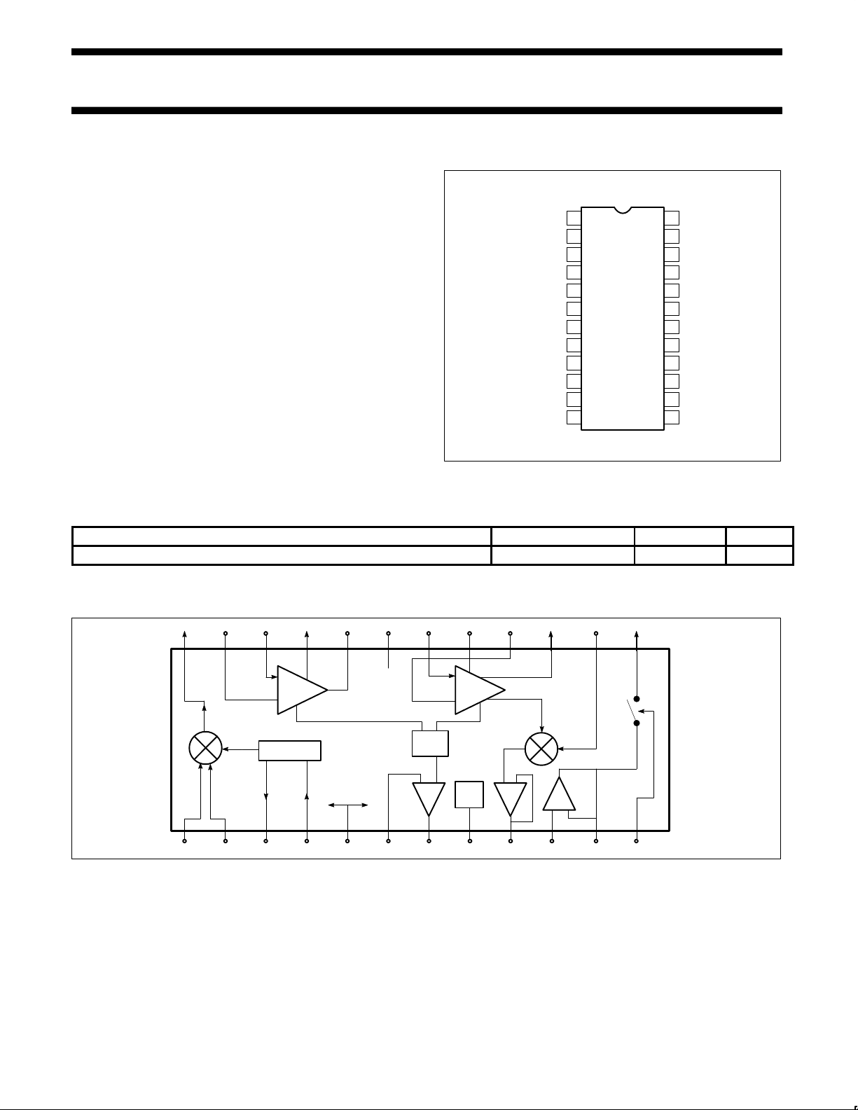
PIN CONFIGURATION
RF
IN
RF BYPASS
XTAL OSC (EMITTER)
XTAL OSC (BASE)
IF AMP DECOUPLING
IF AMP OUT
GND
LIMITER IN
SWITCH OUT
POWER DOWN CONTROL
POSTAMP IN
POSTAMP OUT
SWITCH CONTROL
MIXER OUT
IF AMP IN
LIMITER DECOUPLING
LIMITER DECOUPLING
LIMITER OUT
QUADRATURE IN
V
CC
RSSI FEEDBACK
RSSI OUT
DATA OUT
1
2
3
4
5
6
7
8
9
10
11
12
13
14
24
23
22
21
20
19
18
17
16
15
IF AMP DECOUPLING
UPDATE for 638
SR00907
Figure 1. Pin Configuration
ORDERING INFORMATION
DESCRIPTION TEMPERATURE RANGE ORDER CODE DWG #
24-Pin Plastic TSSOP (Thin Shrink Small Outline Package) -40 to +85°C SA638
SOT-355
BLOCK DIAGRAM
20 19 18 17 16 15 14 132124
10987654321
FAST
IF
AMP
E B
OSCILLATOR
MIXER
QUAD
+–
RSSI
GND
PWR
DWN
RSSI
DATA
V
CC
23 22
1211
LIMITER
+ –
+ –
UPDATE for 638
SR00908
Figure 2. Block Diagram
Page 2
Philips Semiconductors Preliminary specification
SA638IS-54 IF receiver
1995 Feb 16
2
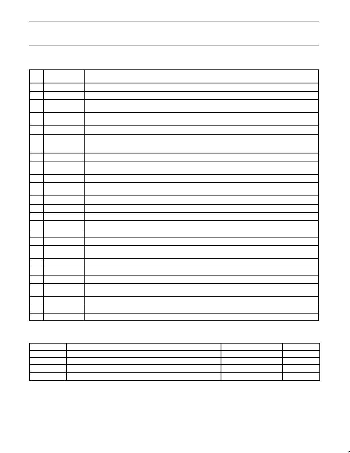
PIN DESCRIPTIONS
Pin
No.
Mnemonic Function
1 RF
IN(+)
RF Input Plus: Differential RF Plus input to mixer.
2 RF
IN(–)
RF Input Minus: Differential RF Minus input to mixer.
3 OSC
B
LO Oscillator Transistor Base: LO generator (Pins 3 and 4) with internal buffer to drive mixer differentially. Can
also be driven externally.
4 OSC
E
LO Oscillator Transistor Emitter: Pins 3 and 4 are used to form an oscillator with external components (tank,
varactor, etc.).
5 V
CC1
Supply Voltage 1: Voltage supply for mixer and main bias.
6 RSSI/AGC
RSSI Out and AGC Input: Dual use: RSSI output in AMPS mode (no internal opamp) and AGC input in QPSK
mode if needed. If no AGC, input will auto AGC to pre-defined fixed level for IQ outputs, in which case this pin
also serves as RSSI output.
7 PWRDWN Power-Down: Chip power-down input (CMOS compatible).
8 OSC
DEMOD
IF Oscillator Input (LO frequency x4): Oscillator input x4 for I/Q demodulation is needed for internally
generating quad LOs by division.
9 ModeSW Mode Switch: Logic control signal to select between AMPS and QPSK modes of operation.
10 AUDIO/LPF
Audio Out and LPF Corner Frequency Control: Dual Use: Audio output in the AMPS mode and LPF corner
frequency control in QPSK mode.
11 DEMOD1 Demod Auxiliary Pin: Used to implement FM demodulation in AMPS mode.
12 Q Baseband Q Ouptut: Quadrature baseband output referenced to IQ
REF
.
13 I Baseband I Output: In-phase baseband output referenced to IQ
REF
.
14 V
CC2
Supply Voltage 2: Voltage supply for IF amp and demodulator.
15 IQ
REF
I/Q Reference Voltage: Reference voltage for baseband I/Q outputs.
16 GND2 Ground 2: Ground common for IF amp and demodulator.
17 DEMOD2/Offsets
Demod Auxiliary Pin and I/Q Offset Control: Dual Use: In AMPS mode serves for FM demodulator; in QPSK
mode serves as I/Q offset control.
18 IQ DEMOD Input to the Demodulator: IF input to demodulator from AGC IF amp output.
19 GND1 Ground 1: Ground common for mixer and main bias.
20 IFAMP
OUT
IF Amplifier Output: IF amplifier output.
21 V
CCMID
VCC Midpoint Bypass: The internally generated VCC midpoint bias needs to be externally bypassed with a
suitable capacitor.
22 IFAMP
IN
Input to IF Amplifier: Input to IF Amplifier from mixer through external filter .
23 IFAMP
DC
Reference Input to IF Amp: External bypassing for low frequency feedback of IF amp to null DC offsets.
24 MIX
OUT
Output from Mixer: IF output from mixer to external BPF and IF amp.
ABSOLUTE MAXIMUM RATINGS
SYMBOL PARAMETER RATING UNITS
V
CC
Single supply voltage V
V
IN
Voltage applied to any other pin V
T
STG
Storage temperature range
°C
T
A
Operating ambient temperature range SA639
°C
NOTE: θJA Thermal impedance (DH package) 117°C/W
Page 3
Philips Semiconductors Preliminary specification
SA638IS-54 IF receiver
1995 Feb 16
3
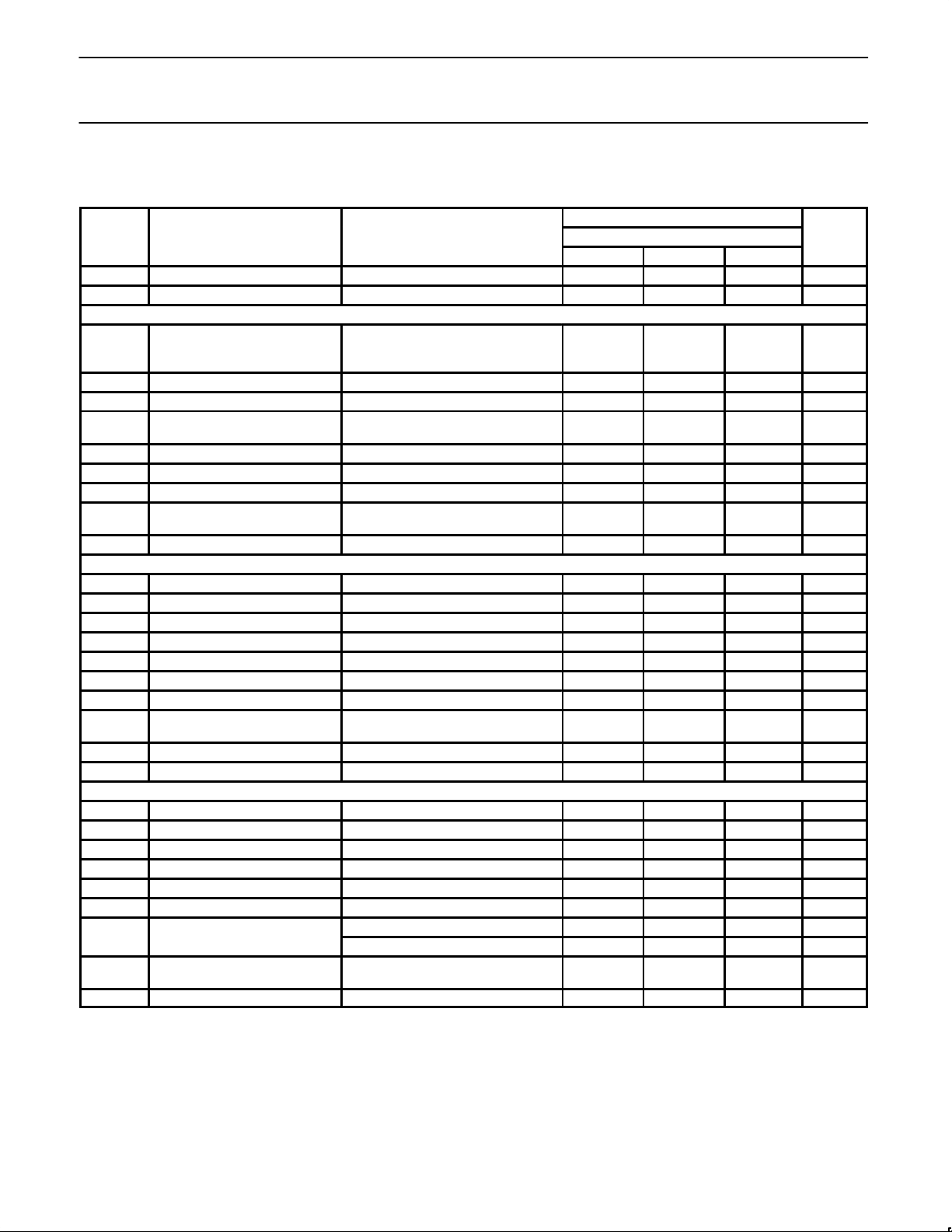
DC ELECTRICAL CHARACTERISTICS
VCC = +3V, TA = 25°C; unless otherwise stated.
LIMITS
SYMBOL
PARAMETER
TEST CONDITIONS
SA639
UNITS
MIN TYP MAX
V
CC
Power supply voltage range 2.7 5.5 V
I
CC
DC current drain 10 mA
Mixer
Conversion power gain
Input matched externally to tbdΩ,
Output is doubly terminated filter,
1.5kΩ impedance
15 dB
Noise figure Single side band 8.5 dB
IIP3 Input IP3 -10 dBm
Input P-1, input compression
point
-20 dBm
Input impedance 1kΩ series with 2.5pF
IF output impedance 1.5 kΩ
Input frequency range 150 MHz
LO and 2xLO suppression at IF
output
-30 dBc
IF frequency 2 MHz
IF Amp, FM Demodulator, RSSI in FM Mode
IF amp gain 90 dB
Input impedance 1.5 kΩ
Output impedance 150 Ω
RSSI dynamic range 90 dB
RSSI linearity -1.5 +1.5 dB
Audio output impedance 300 Ω
Audio output level 110 mV
RMS
Audio SINAD for RF signal
-50dBm
35
Noise figure 11 dB
Output IP3 tbd
IF Amp, AGC, RSSI and IQ Demodulator, QPSK Mode
Input impedance 1.5 kΩ
Gain 10 95 dB
Input IP3 tbd
RSSI dynamic range 90 dB
RSSI linearity -2.5 +2.5 dB
LPF frequency control 40 80 kHz
Channel matching: gain 1 dB
phase 5 deg.
I/Q output level
for a given tbd linearity; about IQ
output reference level
250 mV
PEAK
I/Q output reference level tbd
NOTE:
1.
Page 4

Philips Semiconductors Preliminary specification
SA638IS-54 IF receiver
1995 Feb 16
4
CIRCUIT DESCRIPTION
The Mixer
The mixer section converts signals up to 150MHz to a 2nd IF of up
to 2MHz (typically around 455KHz) with a power gain of 15dB, input
IP3 of –10dBm and NF of 8.5dB. This section is comnlon to both
modes of operation. An on–chip oscillator is provided (for use with
an external tank, varactor, and synthesizer). The LO section has a
buffer to drive the mixer differentially.
After external bandpass filtering, the signals enter the chip again into
the IF amplifier section. One input of the IF amp is biased to V
ccmid
(which is Vcc/2 generated internally and by–passed externally) and
AC-coupled to the input signal externally while the other IF amp
input is fed back from the amplifier output and AC by–passed to
ground externally. This minimizes low frequency offsets since the
amp is DC-coupled with very high gain.
(Note that, compared to our standard 6xx IF chips, we are freeing
quite a few pins by using only 1 decoupling pin and by NOT splitting
up the IF amp into 2 parts and going in and out for filtering in
between.
In the AMPS mode the amplifier acts as a classic limiter with a fairly
constant output voltage for a very large input voltage range. The
RSSI (Received Signal Strength Indicator) is a temperature
compensated high impedance output signal which acts as a voltage
proportional to Logarithm of the input power and has a 90dB
dynamic range. In the Digital mode the IF amp acts as a linear AGC
(Automatic Gain Controlled) amplifier with maximum gain of 95dB
and an AGC range of 85dB. The control for the AGC can be derived
internally or supplied externally. If not supplied externally the
internal AGC detector will regulate the gain to set the IQ baseband
outputs to a pre–determined level (e.g., 250mV
PEAK
). The RSSI
output which is high impedance will then be available at Pin 6 after
external filtering. On the other hand an external AGC input can
force the voltage at this pin to regulate the gain externally based on
external measurement of say the IQ baseband output voltages. In
such a case the RSSI function is NOT provided by this pin. (This
has been done mainly to conserve pins. Depending on customer
feedback we can provide for separate RSSI output and AGC input
pins if necessary.)
The IQ Demodulator Section
The IQ Demodulator section takes the signal after external filtering
fronl the chip’s IF anlp output. The I/Q LO is supplied to the chip
externally as a x4 of the required correct LO signal such that the
internal divider can generate quadrature LO signals of the correct
frequency. After conversion to baseband the signals are filtered for
suppressing LO and its by–products. (We have to decide if this filter
will also provide for accurate baseband filtering. For example TI’s
ARCTIC baseband processor chip provides for such filtering in
which case we do not have to provide for it.) After buffering, the
single ended baseband IQ outputs are available for processing
externally. The signals are referenced to a fixed DC level generated
internally and available througn Pin 15. We can save a pin if the
V
ccmid
(Pin 21) can be used for this purpose. Single-ended outputs
as described above are used rather than differential outputs in order
to save pins.
The FM Demodulator section
The FM Demodulator section will incorporate a new technique wnich
will not require a quad tank. However, a backup technique of the
quad discriminator will be available if the new riskier approach fails.
Because of this, two pins have been allocated for the FM
demodulator in addition to the audio output (similar to our existing
FM–IF products).
In this pinout there is provision for 2 V
CC
pins and 2 ground pins in
addition to a V
CC
/2 bypass pin. This seems necessary in light of the
hign gain values involved in the IF amp block.
There are at least three pins which have dual functionality:
RSSI/AGC; Audio/LPF; Demod2/ IQ Offsets. We have to carefully
look at this to see if this is feasible. If not, the pinout has to be
changed appropriately.
Fallback Positions:
1. We have a fallback for the FM demodulator, the classic FM
discriminator.
2. If the “one IF amp will work for both modes’’ approach fails, we
can provide 2 separate IF amp paths and switch between them
for the different modes. The penalty is increased chip area.
3. The proposed solution for the lF amp is to have all its gain in one
section with no external filtering in between. This is aggressive
since our existing chips have 2 IF sections with separate DC
feedback for each section and external filtering in between. If the
proposed 1 section solution fails, going back to our old technique
will require more pins than we perhaps have!
Page 5
Philips Semiconductors Preliminary specification
SA638IS-54 IF receiver
1995 Feb 16
5
C48 C42
C49
C43
C52
C51
IF BPF
OPTIONAL
BPF
Vcc
IF AMP DC
Vcc
MIXOUT IF AMP IN Vmid IF AMP OUT GND1 IQ DEMOD
DEMOD2/
OFFSETS GND2
IQ REF
VOLTAGE Vcc2 I
RF _RF OSCB OSCE
Vcc1
RSSI/AGC IN PWRDWN
DEMOD
OSC x4
MODE
SWITCH
AUDIO/
LPF
DEMOD1
Q
IF AMP
LIMITER/
AGC
R38
r=R1
MIXER
LO OSC
& BUFFER
AGC
DETECTOR
FROM IF AMP
+IN
–IN
OUT
R35
r=R1
Vcc/2
BIAS GEN
–OUT
+OUT
I–MIXER
Q–MIXER
GmC
LPF
PWRDWN
MODE
CONTROL
FM
DEMOD
DIVIDE /4
90 PHASE
LOW FREQUENCY
FEEDBACK TO NULL
DC OFFSETS
Gm–C
LPF
24 23 22 21 20 19 18 17 16 15 14 13
1 2 3 4 5 6 7 8 9 10 11 12
SR00909
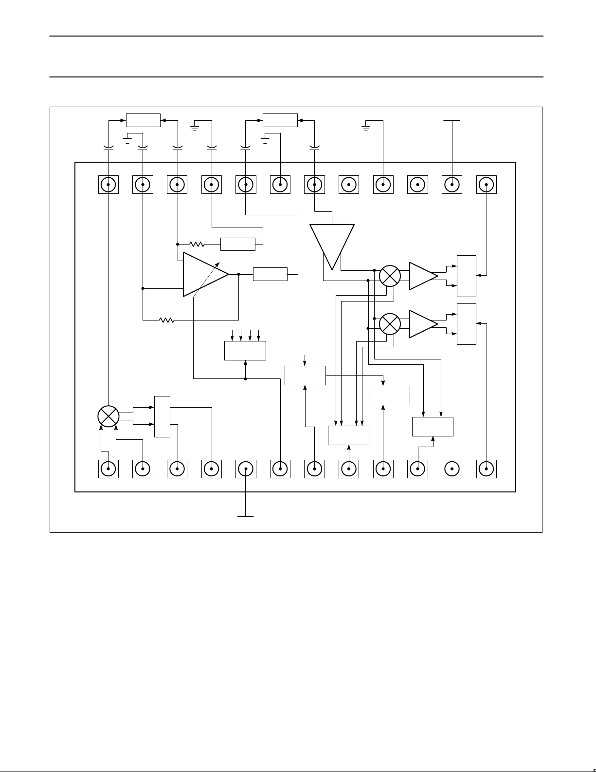
Figure 3. SA638 IS-54 Dual-Mode IF Chip
 Loading...