

Page 1
FEATURES
ROW6
COL1
MFOUT
MUTE
COL7
ROW1
COL2
ROW2
COL3
ROW7
COL4
COL5
ROW4
ROW3
sames
WITH DEDICATED KEYS FOR 20 MEMORIES
SA589
LD/DTMF SWITCHABLE DIALLERS
n Selectable Loop-Disconnect or DTMF
Modes
n Keypad Switchable LD to DTMF
n 20 x 24-Digit Memories, (each with
Dedicated Key)
n 24 Digit Last Number Redial
n Selectable Make/Break Ratios 2:1 and 3:2
DESCRIPTION
The SA589 family are keypad switchable LD/
DTMF dialler devices with a last number
redial facility and twenty 24-digit memories
each with its own dedicated dialling key.
Three operating modes are available: LD
only mode, DTMF only mode and LD mode
with the ability to switch temporarily to DTMF
mode from the keypad during a call. This last
mode enables subscribers to access such
services as home banking. Mixed LD and
DTMF numbers can also be stored in memory.
The SA589 devices are pin compatible with
the SAMES switchable dialler families SA541,
SA545, SA585, SA587 and SA588 - providing
a complete range of telephone features within
a single PCB and circuit design. Metal mask
and pin selectable options are available to
service specific requirements of particular
countries and customers.
n Uses Inexpensive 560kHz Ceramic
Resonator
n Batteryless operation - Low Power CMOS
n Mask Programmable Options to suit
application
n Timed Break Recall (Flash) and Earth
Recall
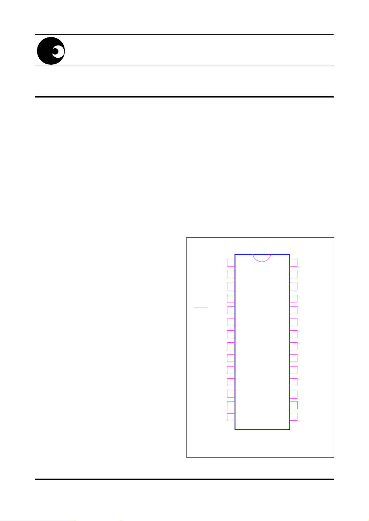
FIG. 1 PIN CONNECTIONS
SA589
NC
COL6
IMP
SELECT
MASK
OSC OUT
OSC IN
FILT IN
FILT OUT
HSW
V
SS
V
DD
PAUSE OUT
ROW5
1
2
3
4
5
6
7
8
9
10
11
12
13
14
28
27
26
25
24
23
22
21
20
19
18
17
16
15
DR-00684
Package: DIP28
1/14
4120 PDS039-SA589-001 REV. C 09-03-1995
Page 2
SA589 FAMILY
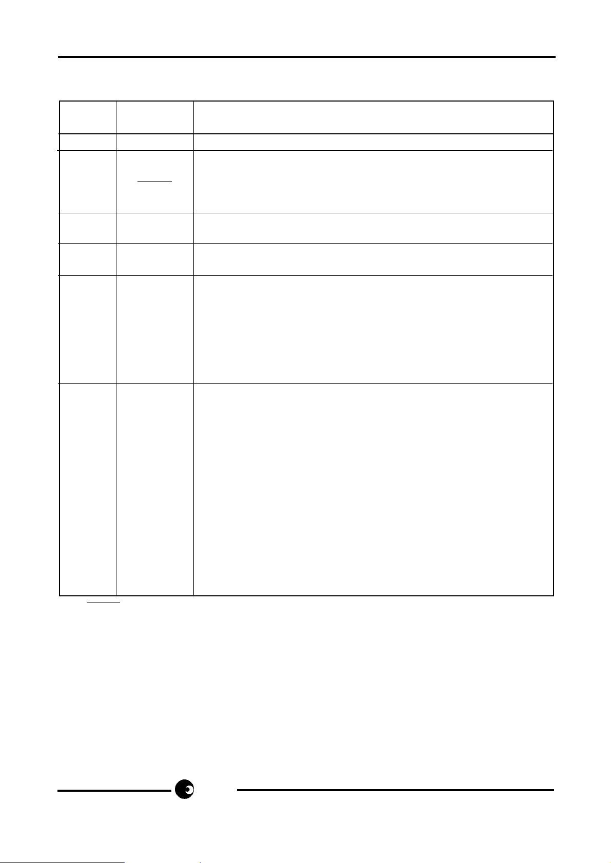
TABLE 1: PIN FUNCTIONS
Pin Pin
number name
Function
1 NC Not connected
3 IMP 'Loop disconnect' dialling output
4 SELECT LD/DTMF selection, IDP and B/M ratio programming
5 MASK Output to disable speech circuit during pulse dialling and recall
(see note 1)
6 OSC OUT Connections for 560kHz ceramic resonator
7 OSC IN
8 FILT IN Unity gain amplifier input and output for DTMF tone filtering
9 FILT OUT
10 HSW Hookswitch input - a logic 1 at this pin is used to indicate 'Off-
Hook'
11 V
12 V
SS
DD
Negative supply
Positive supply
13 PAUSE OUT Active high indicating a pause when dialling from memory
17 MF OUT Unfiltered DTMF output
18 MUTE Output active during keying and tone transmission (see note 2)
19 COL1
20 COL2
21 COL3
26 COL4
27 COL5
2 COL6
16 COL7
22 ROW1 Connections for 38 key single contact keypad
23 ROW2
24 ROW3
25 ROW4
14 ROW 5
15 ROW 6
28 ROW 7
1. MASK may be used to disconnect the whole speech circuit in order to maintain the break
condition whilst on-hook and during a TBR (Timed Flash) operation.
2. MUTE is provided to disable the microphone while maintaining the loop during DTMF
transmission.
OPERATION
Power-on
When power is applied to the chip, a power-on reset circuit operates and ensures that the
Memories are cleared and all logic is reset. The power-on reset circuit is designed such that
if the chip supply voltage drops to a level at which the memories may be corrupted, it will
always, under all conditions, clear the memory, so that corrupt data is not retained.
2/14
sames
Page 3

SA589 FAMILY
Hookswitch Operation
The HSW input is used to inform the SA589 of whether the telephone is on or off hook. Logic
'0' is recognised as on-hook. Logic '1' is recognised as off-hook. When the HSW input rises
from '0' to '1' the off-hook state is recognised immediately and keypad inputs are accepted.
However, when the HSW input falls from '1' to '0' the on-hook state is not recognised for 200
- 300ms. This is so that short line breaks of less than 200ms, such as the line reversals applied
by the exchange, are ignored. In this case the IMP and MASK outputs will go low immediately
the HSW input goes low in order to preserve current, but will resume normal operation
immediately HSW goes high.
On-hook state
In the on-hook state all chip outputs are set low, the oscillator circuit is inhibited and no key
inputs are accepted. This conserves supply current so that the MEMORY contents may be
retained.
Off-hook state
When the HSW input goes high, the MASK output immediately goes to the logic '1' level and
remains there until going on-hook or signalling a TBR, (see timing diagram). COLUMN
outputs also go high until a key is pressed and are normally off whenever timing functions are
not required.
Keypad Operation
A Single Contact, Normally Open keypad is required. When off-hook the COLUMN outputs
are normally held high and the ROW inputs are low. When a key is pressed this connects a
COLUMN output to a ROW input and the ROW input is pulled high.
This action initiates keyboard scanning. During keyboard scanning, the COLUMN outputs
are normally low but generate scanning pulses at 7ms intervals on each output in sequence.
A key is accepted as valid when two successive scanning pulses from the same COLUMN are
seen on a ROW input. Hence, the minimum bounce-free key closure period which is
necessary to guarantee detection is about 14ms (plus the oscillator start-up time if it was not
already running).
Simultaneous key depressions
If two keys are pressed simultaneously (i.e. a second key is pressed before the first has been
verified) neither key will be accepted until both keys are released and the correct key is pressed
again.
Dialling Mode Selection
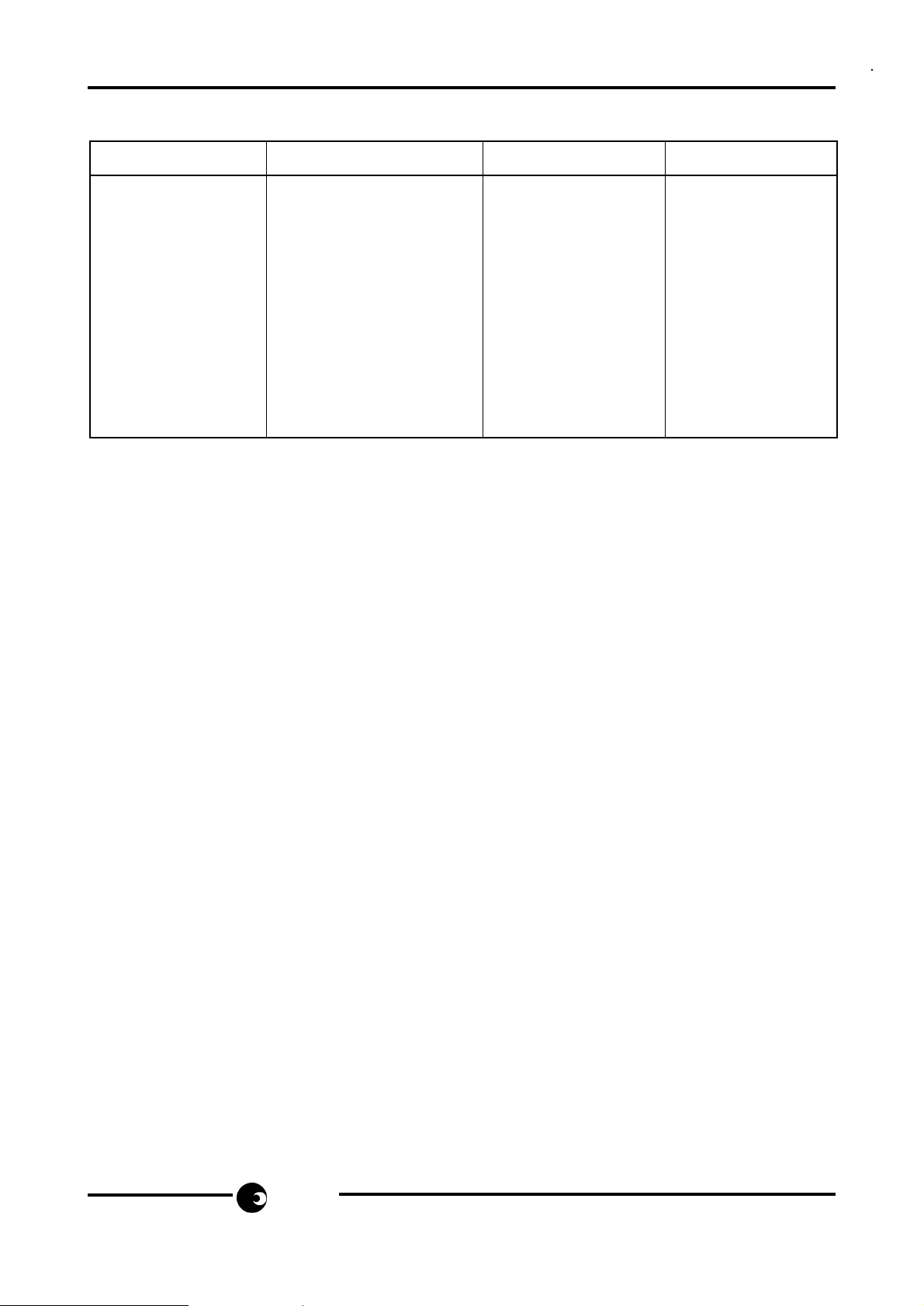
The dialling mode may be selected via the SELECT pin (Pin 4) as detailed in Table 2. Four
'Loop-Disconnect' + DTMF options, two 'Loop-disconnect only' options and three DTMF
modes are available. Each mode offers a different combination of LD and/or MF timing. If
one of the 'LD only' or DTMF only modes is selected then dialling will remain fixed in LD mode
or DTMF mode respectively.
sames
3/14
Page 4
SA589 FAMILY
COL COL COL COL COL COL COL
123 4 5 67
ROW 1 1 2 3 TBR S01 S02 S03
ROW2 4 5 6 REDIAL S04 S05 S06
ROW3 7 8 9 STORE S07 S08 S09
ROW4 * 0 # SHIFT S00 LNR
PAUSE/
CONT
ROW5 S11 S12 S13
ROW6 S10 S14 S15 S16
ROW7 S17 S18 S19
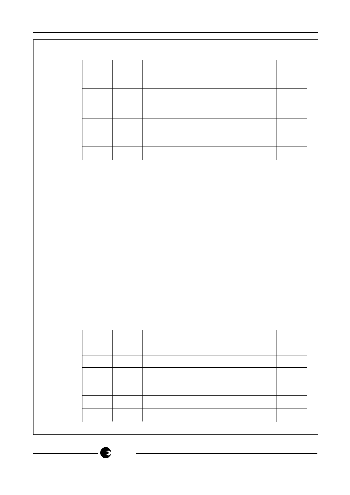
Fig. 2a Versions without TONE key
* or */# are used to change from LD to DTMF dialling and are available as digits when in DTMF
mode.
TBR: Timed Break Recall (Flash).
STORE: Memory Programming key. Use in conjunction with dedicated memory keys or a
two-digit code representing the number of the memory to be programmed
S00-S19: 'Single touch' dedicated memory dialling keys
LNR: Last Number Redial
REDIAL and SHIFT: These keys are clearly unnecessary where keypad positions are
provided for all the dedicated memory keys but may be useful to access memories in
applications where the telephone provides insufficient keys for all these functions. For a
description of the function of the REDIALand SHIFT keys, see the SA585 and SA587 data
sheets, respectively. Do not fir keys in these positions if not required.
PAUSE/CONT: Insert pause in memory/continue dialling
TONE: Change dialling mode from LD to DTMF
COL COL COL COL COL COL COL
123 4 5 67
ROW 1 1 2 3 TBR S01 S02 S03
ROW2 4 5 6 REDIAL S04 S05 S06
ROW3 7 8 9 STORE S07 S08 S09
ROW4 * 0 # TONE SHIFT S00 LNR
ROW5 S11 S12 S13
ROW6 S10 S14 S15 S16
ROW7 S17 S18 S19
Fig. 2b Versions with TONE key
Fig. 2 Keypad layout and connections
4/14
sames
Page 5
SA589 FAMILY
TABLE 2: Dialling mode selection
Select Pin to Dialling Mode B:M Ratio TBR (msec)
V
SS
LD + DTMF 2:1 100
COL1 LD + DTMF 2:1 270
COL2 LD + DTMF 3:2 270
COL3 LD + DTMF 3:2 100
COL4 LD only 2:1 COL5 DTMF only - 270
COL6 DTMF only - 270
COL7 LD only 3:2 -
V
DD
DTMF only - 100
However, if one of the 'LD + DTMF' modes is selected the chip will be in LD mode initially in
the off-hook condition but may be switched to DTMF by pressing either *, */# or TONE key
(depending on the mask variant - see Fig. 2 and page 11), provided that dialling is not in
progress. If any of these keys are pressed during LD dialling, they will be ignored.
Only if * or # are pressed subsequent to switching to DTMF, will * or # be dialled. Only digits
entered prior to a switch to DTMF will subsequently be available for redialling (see Last
Number Redial operation), unless specified otherwise.
Once switched to DTMF, dialling will remain in this mode until either a Recall (Flash) operation
or until the chip returns to the on-hook state.
Last Number Redial (LNR)
The function of the on-chip LNR store is to retain automatically a manually dialled number for
redialling later. The capacity of the memory is 24 digits. If a number is dialled which is longer
than this, dialling will continue, but redialling will not be allowed with this number. To redial
a number in the LNR store, the LNR key may be pressed once, or the Redial key can be
pressed twice.
The last number redial store has several features designed to assist the user:
Moving cursor facility
This facility is provided to aid use in PABX applications, where the user must first dial an
access digit, or digits, and then wait for a second dial tone before continuing dialling.
This allows a user to enter the first digit or digits of the number in the last number redial store
manually before pressing the LNR key; the remainder of the number will be dialled when
the LNR key is pressed.
If the digit(s) dialled manually do not match those in the LNR memory, then redialling will
be inhibited for the remainder of the call, and the numbers entered will be saved in the LNR
memory for redialling in a subsequent call.
If the user manually dials the first digit(s) in the LNR memory, and then goes on-hook, the
whole contents of the memory will be retained.
sames
5/14
Page 6

SA589 FAMILY
Mixed Mode Calls
In the case of a call which starts in LD mode and is switched by the user (via the *, */#, or
TONE key) to DTMF mode, only the digits dialled in LD mode will be retained. This feature
is provided to ensure security of PIN (Personal Identification Number) codes. Provided that
the number of digits dialled in LD mode does not exceed 24, they will be retained regardless
of the number of DTMF digits entered subsequently.
Memory Dialling
The SA589 provides 20 memories, each of which has a capacity of 24 digits and each of which
has its own dedicated key . The memories can save digits for dialling in LD, DTMF and Mixed
Modes and can include pauses if desired.
Programming Memories
The SA589 must be 'off-hook' and idle:
1. Press the STORE key.
2. Press the key (S00 - S19) of the memory to be programmed.
3. Enter digits to be stored (no digits will be dialled whilst programming).
4. To finish programming the memory either press the STORE key again or go 'on-hook'.
5. Repeat to programme other memories.
If more than 24 digits are entered while programming a memory, then the memory will be
cleared until reprogrammed. If any non-valid keys are pressed during programming
(e.g.LNR, TBR) they will be ignored.
Mixed mode numbers and Pauses in memory
Mixed mode (i.e. LD + DTMF) numbers are easily programmed into memory. The SELECT
pin should be set to one of the 'LD + DTMF' modes (as it would be when dialling a mixed
mode number), then the number entered using the same procedure as if dialling normally.
The first press of *, */# or TONE (according to the mask variant) will be stored as a 'change
to DTMF' and this will cause all subsequent digits to be sent in DTMF when redialling from
memory.
Similarly, pauses can be stored in memory by pressing the PAUSE key in the appropriate
position when programming.
When redialling from memory, both Pauses and LD to DTMF changeovers will cause dialling
to halt temporarily until the user presses the PAUSE/CONT key. The exception to this rule
is when an LD to DTMF changeover, is stored in the first memory location; in this case,
DTMF dialling will occur immediately when memory dialling is invoked - this allows DTMF
codes to be easily stored and sent even in a telephone where the normal dialling mode is
LD.
It should be noted that a Pause or an LD to DTMF changeover each require one memory
location.
6/14
sames
Page 7
SA589 FAMILY
Dialling from memories
The SA589 must be 'off-hook' and idle:
1. Press the appropriate memory key (S00 - S19). Dialling will now start.
2. If dialling halts due to a Pause or an LD to DTMF changeover in the memory, the PAUSE
OUT pin will go high (logic '1'). Further dialling can be resumed by pressing the PAUSE/
CONT key or alternatively, by pulling the Column 4 pin low (for a minimum of 14 ms)
to achieve the same result thus allowing an external timer circuit to be used. The
PAUSE OUT output is reset when dialling resumes.
All keypad positions are disabled whilst memory dialling is in progress.
Timed Break & Earth Loop Recall
The SA589 supports both TBR and ELR and offers a common operating protocol in both
cases.
After a recall (Flash) operation, the dialling mode selected via the SELECT pin will be restored.
Also, only the digits dialled after the ELR/TBR operation will be retained in the LNR store
(2)
A TBR (Flash) of 100ms or 270ms
is generated when the TBR key is pressed. The MASK
(1)
output goes low in order to produce the line break. When in DTMF mode, the MF OUT output
also goes low for the duration of the break.
.
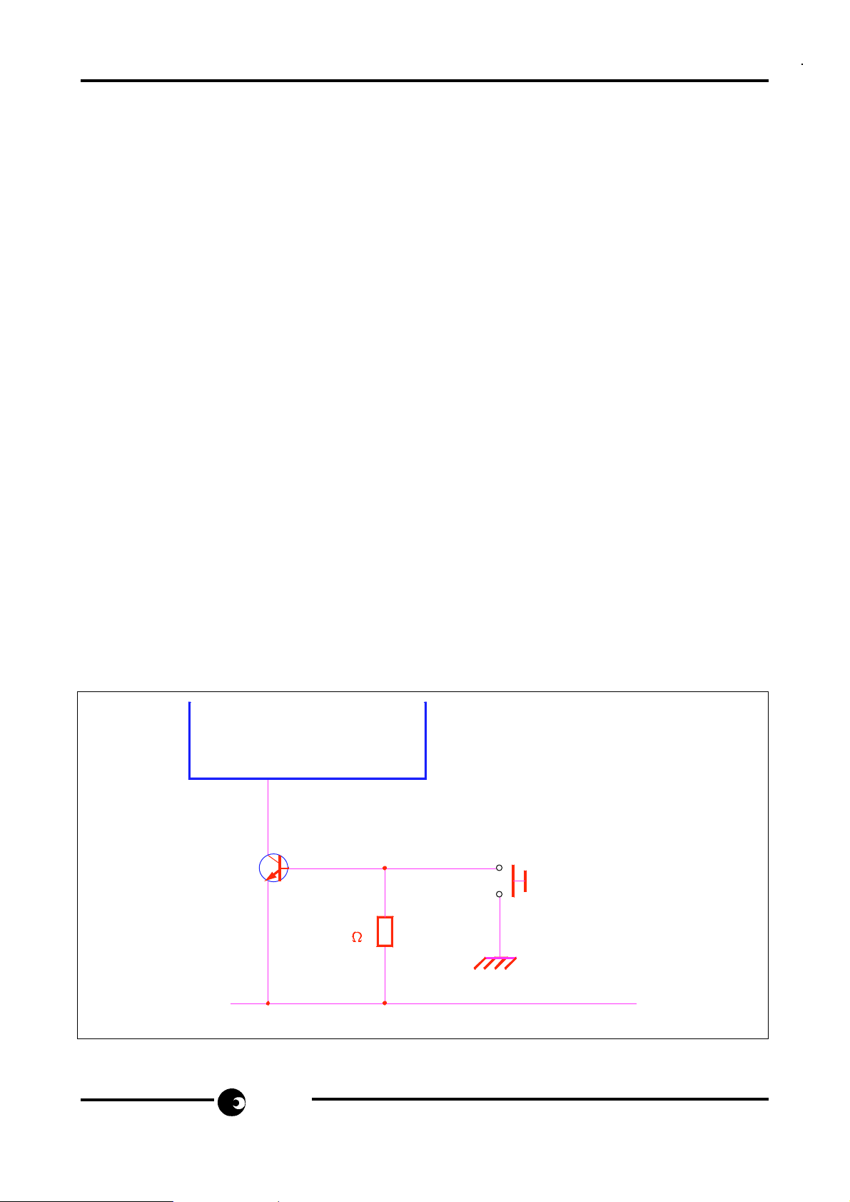
ELR is supported via the column 3 pin. If this pin is connected to ground for a minimum of 20ms
during an ELR operation, the chip will offer the same operating protocol as for TBR.
This may be achieved by use of the circuit shown below in Fig. 3, or by use of a double contact
switch.
(1) Other options are available.
(2) Other TBR (Flash) periods are available as mask options
SA589
21
COL 3
22
DR-00685
sames
Fig. 3 Earth loop recall
7/14
Page 8

SA589 FAMILY
Oscillator Circuit
This requires an external 560kHz ceramic resonator connected between OSC IN and OSC
OUT to provide a timing reference for all chip functions. No other components are required
or should be used.
The oscillator circuit is of the 'single pin' type. Internally, the OSC IN pin is connected to V
SS
and therefore the resonator may alternatively be connected externally between OSC OUT and
V
if desired.
SS
Please consult your resonator supplier who will recommend a suitable resonator type.
Tone Filtering
The spectral purity of the DTMF output is sufficient for most applications. However, where
lower distortion DTMF tones are required, an on-chip darlington pair is provided (accessible
via pins 7 & 8) for use in a low pass active filter.
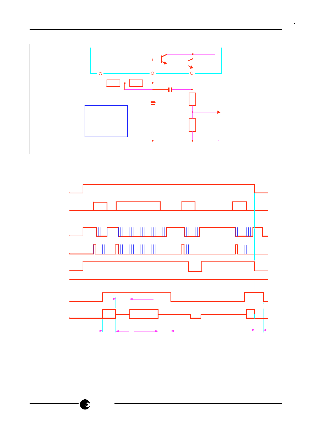
Fig. 4 shows how a 2-pole Sallen and Key filter can be implemented. The typical component
values have been chosen to give a second order Butterworth response with a cut-off frequency
of about 3,5kHz and a nominal pass-band insertion loss of 0.5dB.
DTMF DIALLING
During DTMF dialling the MUTE output goes to logic '1' and remains there for the duration of
the tone transmission.
The IMP output remains low during tone transmission. The MF OUT output rises to its DC level
of 0.9 V
at the start of the tone transmission and is kept there between tone bursts. This is
DD
to avoid transients at the beginning and end of tone bursts.
The maximum rate at which tones are sent to line is 100ms on, followed by 100ms off (unless
specified otherwise). If keys are activated faster than this they are placed in a temporary store
and then sent to line at the maximum rate. Dialling from the LNR memory occurs at the
maximum rate.
If a key is held down for longer than the minimum Tone Burst period, the tone output will
continue until the key is released.
8/14
sames
Page 9
SA589 FAMILY
MFOUT
HOOK SWITCH
SA589
17
R1
Typical values:
R1 = 56k
R2 = 56k
R4 + R3 = 10k
C1 = 1.3nF
C2 = 470pF
DR-00686
Fig. 4 DTMF tone filtering
V
DD
89
FILTIN
R2
Ω
Ω
Ω
C1
C12
FILTOUT
R3
R4
OUTPUT
V
SS
KEY PRESS
COLUMN
ROW
MASK
IMP(LOW)
MUTE
MF OUT
DR-00687
100ms
"5"
"5"
"8"
100ms
"8"
100ms
"TBR"
"9"
"9"SHORTENED
ON HOOK
TIME OUT
Fig. 5 DTMF mode timing diagram
sames
9/14
Page 10
SA589 FAMILY
TABLE 3: Tone Frequencies
Keypad R1 R2 R3 R4 C 1 C2 C 3 C 4
Nominal frequency (Hz) 697 770 852 941 1209 1336 1477 1633
Deviation from nominal (%) -0.07 -0.10 +0.19 -0.15 -0.17 -0.20 -0.22 -0.31
NOTE: There will be an additional frequency error caused by any deviation of the resonator
frequency from the nominal 560kHz.
LOOP DISCONNECT DIALLING
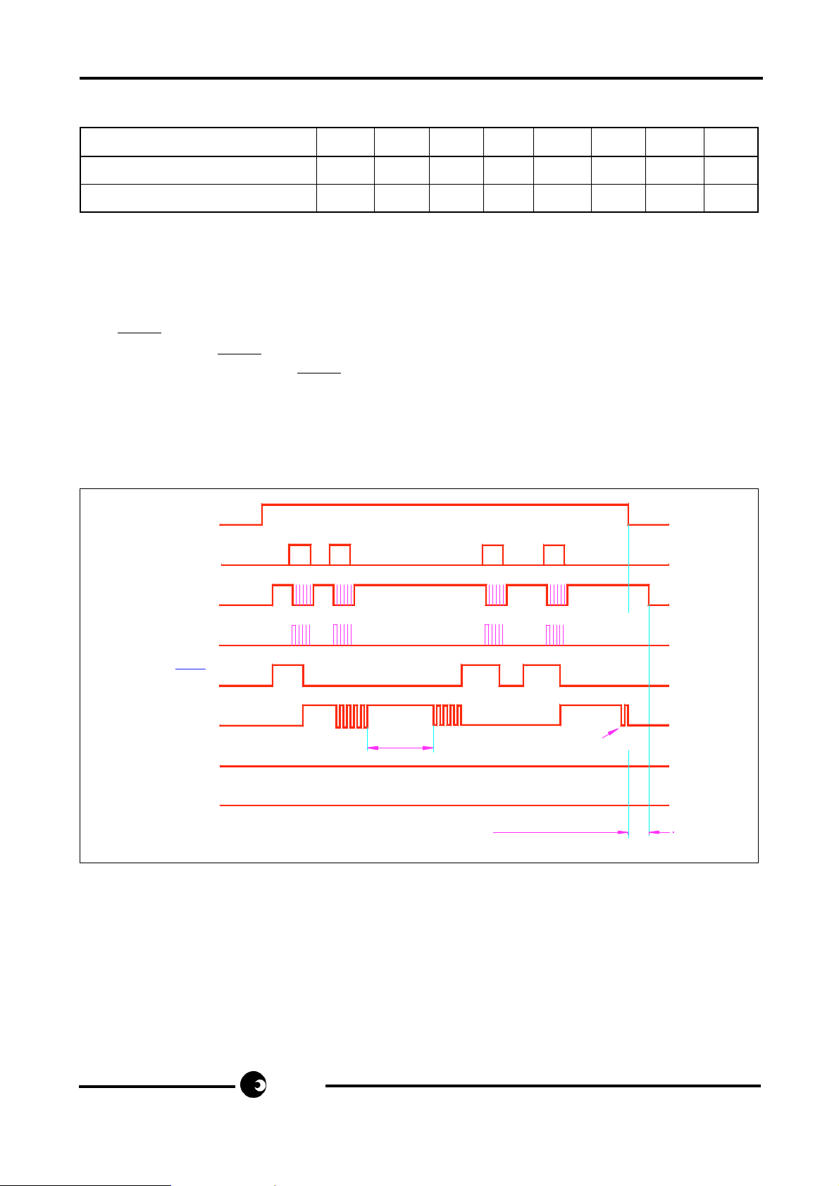
The MASK output is provided in order to disable the speech circuit during LD dialling.
Consequently the MASK output is normally at logic '1' in the off-hook condition, but changes
to logic '0' during LD dialling. MASK also changes to logic '0' in order to signal a Timed Break
Recall (Flash) to the line.
Both MUTE and MF OUT remain low during LD dialling. LD dialling is signalled on the IMP
output. A break is signalled by a logic '0'. Make periods and IDP times are signalled by a logic
'1'. When not dialling, the IMP output sits at logic '0'.
HOOK SWITCH
KEY PRESS
COLUMN
ROW
MASK
IMP
MUTE(LOW)
MF OUT
DR-00688
"5" "8"
"5"
"IDP"
2.2340
"TBR"
"8"
ON HOOK TIME OUT
Fig. 6 LD mode timing diagram
"9"
"9"
(PARTIAL)
10/14
sames
Page 11
SA589 FAMILY
IMP
t=
1
t
=
2
t
=
3
t
=
4
t
=
5
DR-00689
t
1
t
2
t
3
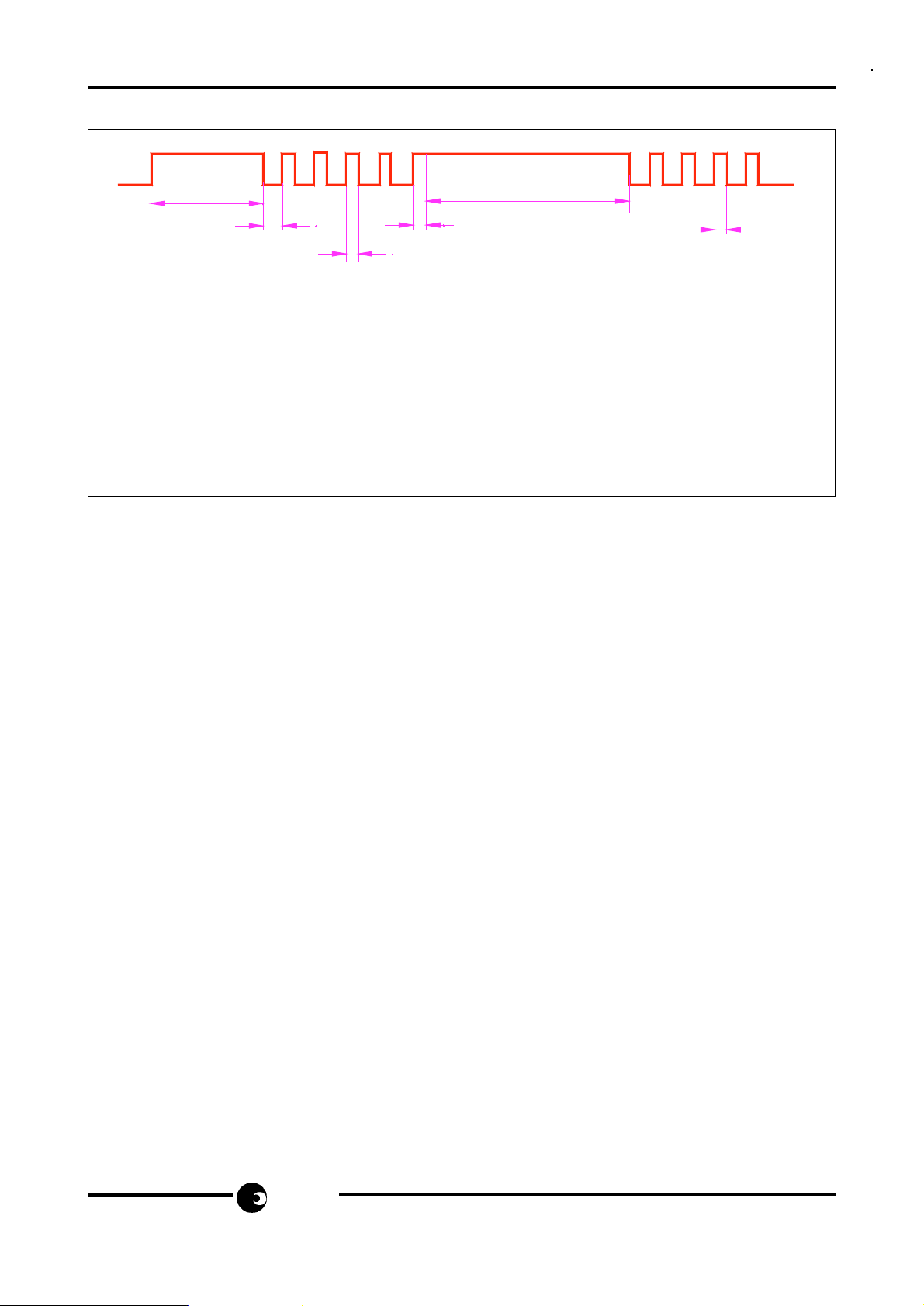
PRE-DIGIT PAUSE (=t )
BREAK PERIOD (60ms or 67ms)
MAKE PERIOD (40ms or 33ms)
POST-DIGIT MAKE (=t )
INTER-DIGIT PAUSE (800ms)
5
3
t
4
t
5
t
3
Fig.7 Timing data
MASK OPTIONS
The SA589 has been designed so that many features can be altered quickly and inexpensively
at the final stage of manufacture. These options allow the telephone manufacturer to cater
for different market requirements throughout the world without changing the telephone circuit.
The options, listed below, are possible in any combination. Standard options are listed first
in bold italics at 'a'. Other options may be produced by arrangement. Please consult your
nearest SAMES Representative for advice on availability.
A. 'Long' TBR (Flash) Period
a. 270ms
b. 600ms
B. LD to DTMF Keypad Switching
a. * and # keys
b. TONE key
c. * key
C. Retention of Post-*/#Digits in LNR Store (DTMF Mode)
a. All digits retained
b. Digits before * or # retained
D. Short/Long TBR Selection
a. As specified
b. Short and Long TBR reversed
E. Recall (Flash)/LNR protocol
a. Digits dialled after Recall retained
b. Digits dialled before Recall retained
sames
11/14
Page 12
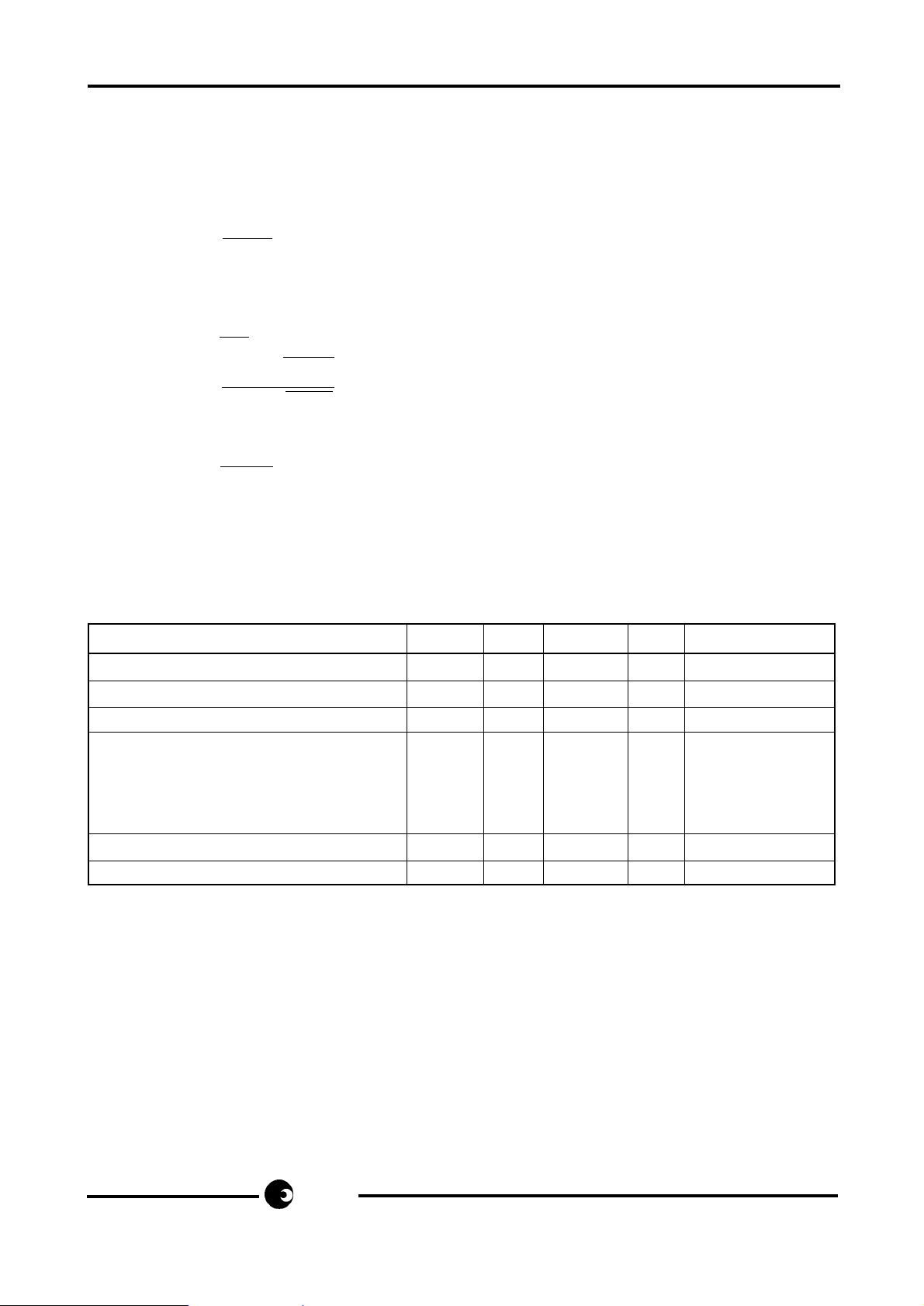
SA589 FAMILY
F. DTMF Minimum Timings
a. 100ms on, 100ms off
b. 85ms on, 85ms off
c. 85ms on, 170ms off
G. Pin 5
a. MASK
b. MASK
H. Pin 3
a. IMP
b. IMP
c. [IMP + MASK]
d. [IMP + MASK]
I. Pin 18
a. MUTE
b. MUTE
J. Pin 13 Function
a. PAUSE OUT
b. SECRECY
ABSOLUTE MAXIMUM RATINGS *
Parameter Min T yp Max Unit Notes
Supply Voltage V
DD
- V
SS
-0,3 6,5 V
Voltage on any pin (except HSW) VSS -0,3 VDD +0,3 V
Voltage on pin HSW VSS -0,3 V See Note 1
Current at any pin -1 1 mA
(except HSW, FILTOUT and FILTIN)
Current at pin FILTOUT 0 0,1 mA
Current at pin FILTIN -5 0 mA
Operating Temperature -2 5 70 °C
Storage Temperature -5 5 125 °C
* Stresses above those listed under "Absolute Maximum Ratings" may cause permanent
damage to the device. This a stress rating only. Functional operation of the device at these
or any other condition above those indicated in the operation sections of this specification, is
not implied. Exposure to Absolute Maximum Ratings for extended periods may affect device
reliability.
Note 1: A diode is internally connected between this pin and VDD. Provided current is externally
limited to 300µA max, no damage will occur.
12/14
sames
Page 13
SA589 FAMILY
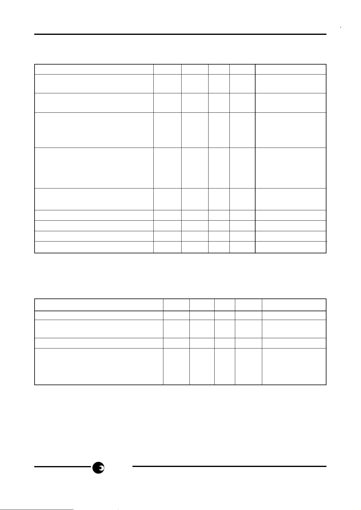
DC ELECTRICAL CHARACTERISTICS
(V
= 2,5V at 25°C, unless otherwise specified)
DD
Condition Min Typ Max Unit Notes
Supply voltage: on-hook 1,8 5,7 V
For memory retention
off-hook 2,4 5,7 V
Hookswitch input:on-hook 0,2 V
off-hook 0,8 V
DD
DD
Supply Current: on-hook <0.2 5 µA VDD = 2.5V (See note 1)
off-hook 1,5 µA See note 1
MF tone sending 1,0 mA If MF OUT is low
LD impulsing 200 µA
Output High Voltage 2,2 V I = -1mA
(MASK, MUTE and IMP Outputs)
Output Low Voltage 0,3 V I = +1mA
(MASK, MUTE and IMP Outputs)
MF OUT d.c. Level During Tone
Sending 0,9V
DD
V
MF OUT Output Resistance 3 KΩ
'Key Pressed' Resistance 2 KΩ 2,5V<V
'Key Not Pressed' Resistance 500 KΩ 2,5V<V
Darlington Pair Current Gain 600 50,000 I
=100µA,Vce=2V
e
<5,7V
DD
<5,7V
DD
NOTE 1: Specially tested versions with guaranteed lower on-hook supply current are
available
AC ELECTRICAL CHARACTERISTICS
(VDD = 2,5V at 25°C, unless otherwise specified)
Condition Min Typ Max Unit Notes
Oscillating Frequency 560 kHz
Tone Output: Low Group 68 77 mVrms No Load
High Group 97 109 mVrms No Load
High-to-Low Group Amplitude Ratio 1,5 2 2,5 dB at MF OUT
Total harmonic Distortion: 0-4KHz 1,5 %
0-10KHz 2,5 %
0-50KHz 5,0 %
0-200KHz 6,5 10 %
sames
13/14
Page 14

SA589 FAMILY
Disclaimer: The information contained in this document is confidential and proprietary to South African Micro-
Electronic Systems (Pty) Ltd ("SAMES) and may not be copied or disclosed to a third party, in whole or in part,
without the express written consent of SAMES. The information contained herein is current as of the date of
publication; however, delivery of this document shall not under any circumstances create any implication that
the information contained herein is correct as of any time subsequent to such date. SAMES does not undertake
to inform any recipient of this document of any changes in the information contained herein, and SAMES
expressly reserves the right to make changes in such information, without notification,even if such changes would
render information contained herein inaccurate or incomplete. SAMES makes no representation or warranty that
any circuit designed by reference to the information contained herein, will function without errors and as intended
by the designer.
South African Micro-Electronic Systems (Pty) Ltd
P O Box 15888, 33 Eland Street,
Lynn East, 0039 Koedoespoort Industrial Area,
Republic of South Africa, Pretoria,
Republic of South Africa
Tel: 012 333-6021 Tel: Int +27 12 333-6021
Fax: 012 333-8071 Fax: Int +27 12 333-8071
14/14
sames
 Loading...