

Page 1
H-BRIDGE MOTOR DRIVER/AMPLIFIER
12345678910
ANALOG
GND
CF
NC
Vcc
+Vs
ANALOG
INPUT
POWER
GND
11
12
DISABLE
ISENSE A
A OUT
B OUT
ISENSE B
PWM
INPUT
*
*
*
*
*
Protection diodes are recommended for
applications where +Vs exceeds 50V.
Required RC network. See paragraph on
transient supression.
‡
‡
‡
MICROTECHNOLOGY
HTTP://WWW.APEXMICROTECH.COM (800) 546-APEX (800) 546-2739
FEATURES
• LOW COST COMPLETE H-BRIDGE
• SELF-CONTAINED SMART LOWSIDE/HIGHSIDE DRIVE
CIRCUITRY
• WIDE SUPPLY RANGE: UP TO 80V
• 10A CONTINUOUS OUTPUT
• ISOLATED CASE ALLOWS DIRECT HEATSINKING
• HIGH EFFICIENCY: UP TO 97%
• FOUR QUADRANT OPERATION, TORQUE
CONTROL CAPABILITY
• INTERNAL/PROGRAMMABLE PWM FREQUENCY
GENERATION
SA60
APPLICATIONS
• BRUSH TYPE MOTOR CONTROL
• CLASS D SWITCHMODE AMPLIFIER
• REACTIVE LOADS
• MAGNETIC COILS (MRI)
• ACTIVE MAGNETIC BEARING
• VIBRATION CANCELLING
DESCRIPTION
The SA60 is a pulse width modulation amplifier that can
supply 10A continuous current to the load. The full bridge
amplifier can be operated over a wide range of supply voltages. All of the drive/control circuitry for the lowside and
highside switches are internal to the hybrid. The PWM circuitry
is internal as well, leaving the user to only provide an analog
signal for the motor speed/direction, or audio signal for
switchmode audio amplification. The internal PWM frequency
can be programmed by an external integrator capacitor. Alternatively, the user may provide an external TTL-compatible
PWM signal for simultaneous amplitude and direction control
for four quadrant mode.
BLOCK DIAGRAM
DISABLE
ANALOG IN
Cf/PWM IN
3
4
2
H-Bridge
Drive
10
11
9
+V
s
B OUT
A OUT
TYPICAL APPLICATION
11
9
SA60
4
3
2
8
12
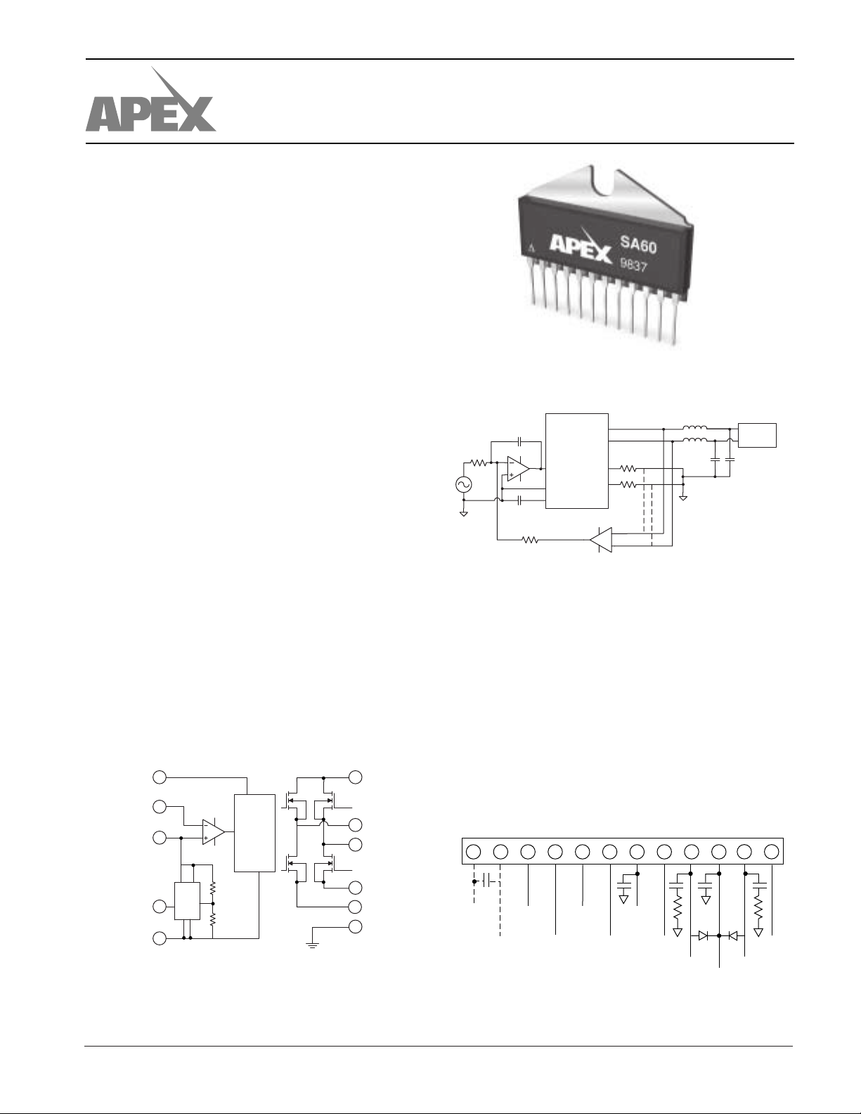
A wide variety of loads can be driven in either the voltage
mode or the current mode. The most common applications use
three external blocks: a low pass filter converting pulse width
data to an analog output, a difference amplifier to monitor
voltage or current and an error amplifier. Filter inductors must
be suitable for square waves at the switching frequency
(laminated steel is generally not acceptable). Filter capacitors
must be low ESR and rated for the expected ripple current. A
difference amplifier with gain of less than one translates the
differential output voltage to a single feedback voltage. Dashed
line connections and a higher gain difference amplifier would
be used for current control. The error amplifier integrates the
difference between the input and feedback voltages to close
the loop.
LOAD
EXTERNAL CONNECTIONS Package: SIP03
2
6
555
8
4
7
49K
2.58K
1
1
7
V
cc
ANALOG GND
APEX MICROTECHNOLOGY CORPORATION • TELEPHONE (520) 690-8600 • FAX (520) 888-3329 • ORDERS (520) 690-8601 • EMAIL [email protected]
8
12
6
A
I
sense
I
B
sense
POWER
GND
Page 2
SA60
ABSOLUTE MAXIMUM RATINGS
SPECIFICATIONS
ABSOLUTE MAXIMUM RATINGS
SPECIFICATIONS
PARAMETER TEST CONDITIONS
INPUT
ANALOG INPUT VOLTAGES Vcc = 12V
A, B OUT = 50% Duty Cycle 1/2VCC Vdc
A OUT = 100% Duty Cycle High 1/3VCC Vdc
B OUT = 100% Duty Cycle High 2/3VCC Vdc
PWM INPUT
PWM PULSE LOW VOLTAGE 0 0.8 Vdc
PWM PULSE HIGH VOLTAGE 2.7 5.0 Vdc
PWM FREQUENCY 45 250 KHz
DISABLE ON 2.7 Vcc Vdc
DISABLE OFF 0 0.8 Vdc
OUTPUT
Vds (ON) VOLTAGE, each MOSFET Ids = 10A 1.7 2.5 Vdc
TOTAL Ron, both MOSFETs .45 Ω
EFFICIENCY, 10A OUTPUT +VS = 80V 91 %
CURRENT, continuous 10 A
CURRENT, peak t = 100 msec 15 A
SWITCHING FREQUENCY Cf = 270 pf 45 KHz
DEAD TIME 90 nS
SUPPLY VOLTAGE, +V
OUTPUT CURRENT, peak 15A
LOGIC SUPPLY VOLTAGE, Vcc 16V
POWER DISSIPATION, internal 156W
TEMPERATURE, pin solder - 10s 300°C
TEMPERATURE, junction
TEMPERATURE, storage –65 to +150°C
OPERATING TEMPERATURE RANGE, case –25 to +85°C
2
S
3
MIN TYP MAX UNITS
80V
1
150°C
POWER SUPPLY
+VS VOLTAGE +VS Current = Load Current 80 Vdc
Vcc VOLTAGE 9.5 12 16 Vdc
Vcc CURRENT Vcc = 12Vdc 28 36 mA
+VS CURRENT Switching, no load, VS = 50V 5 mA
THERMAL
RESISTANCE, junction to case Full temp range, for each transistor 1.6 °C/W
RESISTANCE, junction to air Full temperature range 30 °C/W
TEMPERATURE RANGE, case –25 +85 °C
NOTES: 1. Each of the two active output transistors can dissipate 78W.
CAUTION
3
2. Unless otherwise noted: TC = 25°C, Vcc = 12Vdc.
3. Long term operation at the maximum junction temperature will result in reduced product life. Derate internal power dissipation to
achieve high MTTF. For guidance, refer to the heatsink data sheet.
The SA60 is constructed from MOSFET transistors. ESD handling procedures must be observed.
The exposed substrate contains beryllia (BeO). Do not crush, machine, or subject to temperatures in excess of 850°C to
avoid generating toxic fumes.
APEX MICROTECHNOLOGY CORPORATION • 5980 NORTH SHANNON ROAD • TUCSON, ARIZONA 85741 • USA • APPLICATIONS HOTLINE: 1 (800) 546-2739
Page 3

TYPICAL PERFORMANCE
GRAPHS
SA60
80
POWER DERATING
60
40
20
EACH OUTPUT
TRANSISTOR
0
INTERNAL POWER DISSIPATION, (W)
CASE TEMPERATURE, T (°C)
Vs QUIESCENT VS VOLTAGE
1.8
1.6
1.4
1.2
1
0.8
0.6
0.4
0.2
NORMALIZED QUIES CURRENT (X)
10 7020 30 40 50 60
85°C
Vs, (V)
75
1000 25 50 125
C
25°C
80
TOTAL VOLTAGE DROP
35
30
25
20
15
10
VOLTAGE DROP, V
100
80
60
40
DUTY CYCLE (%)
20
ANALOG INPUT AS PROPORTION OF Vcc
Tc = 110°C
Tc = 85°C
Tc = 60°C
5
0
369
01215
OUTPUT CURRENT, A
Tc = 35°C
DUTY CYCLE VS ANALOG INPUT
A OUT B OUT
0
1/6 5/6
1/3
1/2 2/3
1000
100
CLOCK FREQUENCY, Fsw (KHz)
10
10 100 1000
EXTERNAL INTEGRATION CAP, C (pF)
10
1
FLYBACK CURRENT ISD(A)
0.1
0.6 0.8 1.4
PWM FREQ VS EXT INT CAP
Cf (pF) = (1.44E7/Fsw)–50
REVERSE DIODES
1.2 1.81.6
1
SOURCE TO DRAIN VOLTAGE
Vs QUIESCENT VS SWITCH FREQ
160
140
120
100
80
60
40
20
Vs QUIES CURRENT Iq (mA)
0
0 50 100 150 200 250
SWITCHING FREQUENCY, Fsw (KHz)
Vcc IQ VS SWITCH FREQ
1.6
1.5
1.4
1.3
1.2
1.1
1
0.9
NORMALIZED QUIESCENT, 1q(X)
0.8
25 50 75 100 125
SWITCHING FREQUENCY, Fsw (KHz)
Vcc QUIESCENT VS VOLTAGE
1.4
1.3
1.2
1.1
1
0.9
0.8
0.7
0.6
NORMALIZED QUIES CURRENT, (X)
91610 11 12 13 14 15
Vcc VOLTAGE (V)
APEX MICROTECHNOLOGY CORPORATION • TELEPHONE (520) 690-8600 • FAX (520) 888-3329 • ORDERS (520) 690-8601 • EMAIL [email protected]
Page 4

SA60
OPERATING
CONSIDERATIONS
GENERAL
Please read Application Note 30 on "PWM Basics". Refer to
Application Note 1 "General Operating Considerations" for
helpful information regarding power supplies, heat sinking and
mounting. Visit www.apexmicrotech.com for design tools that
help automate pwm filter design; heat sink selection; Apex’s
complete Application Notes library; Technical Seminar Workbook; and Evaluation Kits.
PWM OSCILLATOR – INTERNAL OR EXTERNAL
The SA60 contains an internal PWM oscillator whose frequency is determined by an external capacitor connected
between pin 1 and pin 2. Maximum frequency is 125 kHz. The
user may also disregard the internal PWM oscillator and
supply the SA60 with an external TTL pulse generator up to
250KHZ.
PIN DESCRIPTION
VCC - is the low voltage supply for powering internal logic
and drivers for the lowside and highside MOSFETS. The
supplies for the highside drivers are derived from this voltage.
V
- is the higher voltage H-bridge supply. The MOSFETS
S
obtain the output current from this supply pin. The voltage on
this pin is limited to +80V by the drive IC. The MOSFETS are
rated at 100 volts.
ISENSE A AND B - These are tied to power gnd directly or
through sense resistors.
ANALOG GND -is the reference for the internal PWM
oscillator. Connect this pin to pin 6. Connect low side of Vcc
supply and any other supply used to generate analog input
signals to ANALOG GND.
ANALOG INPUT - is an analog input for controlling the PWM
pulse width of the bridge. A voltage higher than Vcc/2 will
produce greater than 50% duty cycle pulses out of B OUT. A
voltage lower than Vcc/2 will produce greater than 50% duty
cycle pulses out of A OUT. If using in the digital mode, bias this
point at 1/2 the logic high level.
DISABLE - Is the connection for disabling all 4 output
switches. DISABLE high overrides all other inputs. When
taken low, everything functions normally. An internal pullup to
Vcc will keep DISABLE high if pin left open.
PWM INPUT - Is the TTL compatible digital input for
controlling the PWM pulse width of the bridge. A duty cycle
greater than 50% will produce greater than 50% duty cycle
pulses out of the A out. A duty cycle less than 50% will produce
greater than 50% duty cycle from the B out. For analog inputs,
the integration capacitor for the internal clock must be connected between this pin and analog ground. The internal
switching frequency is programmable up to 125 kHz by selection of the integration capacitor. The formula is:
C
(pF) =
F
1.44 x10
(
Fsw
7
)
– 50
BYPASSING
Adequate bypassing of the power supplies is required for
proper operation. Failure to do so can cause erratic and low
efficiency operation as well as excessive ringing at the outputs.
The Vs supply should be bypassed with at least a 1µF ceramic
capacitor in parallel with another low ESR capacitor of at least
10µF per amp of output current. Capacitor types rated for
switching applications are the only types that should be considered. The 1µF ceramic capacitor must be physically connected
directly to the Vs and POWER GND pins. Even one inch of lead
length will cause excessive ringing at the outputs. This is due
to the very fast switching times and the inductance of the lead
connection. The bypassing requirements of the Vcc supply are
less stringent, but still necessary. A .1µF to .47µF ceramic
capacitor connected directly to the Vcc and ANALOG GND
pins will suffice.
PCB LAYOUT
The designer needs to appreciate that the SA60 combines
in one circuit both high speed high power switching and low
level analog signals. Certain layout rules of thumb must be
considered when a circuit board layout is designed using the
SA60:
1. Bypassing of the power supplies is critical. Capacitors must
be connected directly to the power supply pins with very
short lead lengths (well under 1 inch). Ceramic chip capacitors are best.
2. Connect ANALOG GND to POWER GND with a conductor
having no intermediate connections. Connect all Vs power
supply, filter and load related ground connections to POWER
GND keeping these conductors separate until reaching pin
6. Connect all Vcc power supply and input signal related
ground connections to ANALOG GND keeping conductors
separate until reaching pin 1. Do not allow ground loops to
form by making additional ground connections at the low
side of the physical power supplies. If ground plane is used
do not allow more than 1mA to flow through it.
3. Beware of capacitive coupling between output connections
and signal inputs through the parasitic capacitance between layers in multilayer PCB designs.
4. Do not run small signal traces between the pins of the output
section (pins 8-12).
CURRENT SENSE
There are two load current sensing pins, I SENSE A and I
SENSE B. The two pins can be shorted to POWER GND in the
voltage mode connection but both must be used in the current
mode connection. It is recommended that R SENSE resistors be
non-inductive. Load current flows in the I SENSE pins. The SA60
has no internal current limit.
TRANSIENT SUPPRESSION
An RC Network of A 100 PF Capacitor and a one ohm resistor
is required as shown in the external connection diagram on page
1. This network assures proper operation under various loads.
Minimal power is dissipated in the resistor.
This data sheet has been carefully checked and is believed to be reliable, however, no responsibility is assumed for possible inaccuracies or omissions. All specifications are subject to change without notice.
APEX MICROTECHNOLOGY CORPORATION • 5980 NORTH SHANNON ROAD • TUCSON, ARIZONA 85741 • USA • APPLICATIONS HOTLINE: 1 (800) 546-2739
SA60U REV. E FEBRUARY 2000 © 2000 Apex Microtechnology Corp.
 Loading...