

Page 1
INTEGRATED CIRCUITS
SA5777A
Dual air–core gauge driver
Product specification
Supersedes data of 1997 Feb 24
1999 Sep 20
Page 2
Philips Semiconductors Product specification
SA5777ADual air-core gauge driver
DESCRIPTION
The SA5777A is a monolithic driver for controlling air-core (or
differential) meters typically used in automotive instrument cluster
applications. The circuit interfaces with a microprocessor through a
serial bus and directly drives the air-core meter. The SA5777A has
10-bit resolution (0.35 degree) and is guaranteed to be monotonic.
Data can be shifted through the part, allowing several SA5777As to
be cascaded with only one chip-select line. On-chip current shut
down logic protects the circuit from external faults.
FEATURES
•10-Bit resolution (0.35 degrees)
•Exceptional accuracy (0.5 degrees, typical)
•High-torque capability
•Active differential drivers eliminate back-EMF issues
•No RFI/EMI generation issues
•Simple serial interface
•Simple cascading capability for multiple meters
•Internal fault protection
•Only one external component required (bypass capacitor)
APPLICATION
•Instrumentation utilizing air-core meters
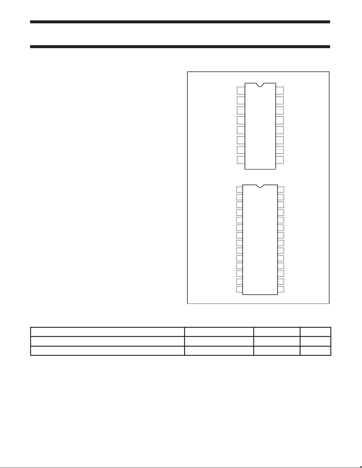
PIN CONFIGURATION
1
C1–
C1+
2
A
3
GND
4
V
BB
DATA
DATA
DATA
DATA
5
OUT
6
IN
V
7
CC
89
OE
1
C1–
C1+
2
3
NC
NC
4
5
NC
6
A
GND
7
V
BB
8
OUT
9
IN
10
NC
NC NC
11
12
NC NC
13
V
CC
OE
14
N Package
D Package
16
C2+
15
C2-
14
COM
13
A
GND
12
D
GND
11
ST
10
CS
S
CLK
28
C2+
C2-
27
NC
26
25
NC
24
COM
23
A
GND
NC
22
NC
21
20
D
GND
19
ST
18
17
16
CS
15
S
CLK
SL00460
Figure 1. Pin configuration
ORDERING INFORMATION
DESCRIPTION TEMPERATURE RANGE ORDER CODE DWG #
16-Pin Plastic Dual In-Line Package (DIP)
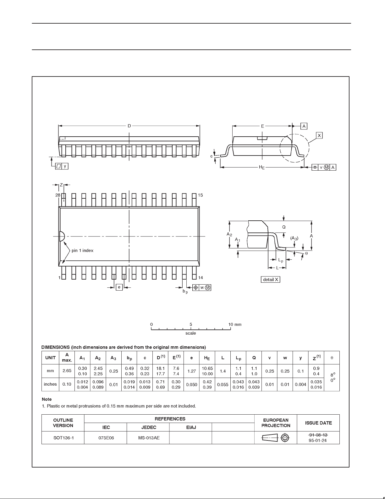
28-Pin Plastic Small Outline Package (SO)
1999 Sep 20 853-1930 022368
2
-40 to +85°C
-40 to +85°C
SA5777AN SOT38-4
SA5777AD SOT136-1
Page 3
Philips Semiconductors Product specification
SA5777ADual air-core gauge driver
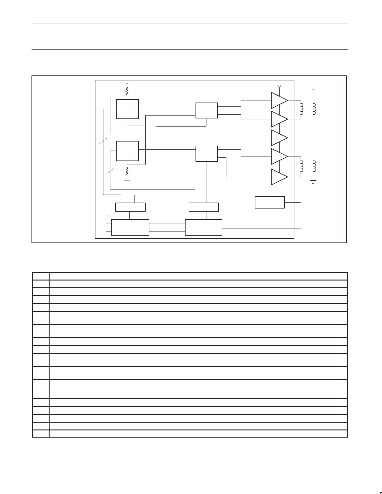
BLOCK DIAGRAM
V
7 + – BIT
DAC
BB
OE
MUX
C2+
C2–
V
BB
8
V
D
S
CS
CC
IN
CLK
7 + – BIT
DAC
8
9-BIT LATCH
10-BIT
SHIFT REGISTER
MUX
9-BIT LATCH
10-BIT
SHIFT REGISTER
Figure 2. Block diagram
Table 1. SA5777A Pin Descriptions for the N Package (Dual In-Line)
Pin # Name Function
1. C1– Negative output connection to the TAN coil of meter #1.
2. C1+ Positive output connection to the TAN coil of meter #1.
3. A
GND
4. V
DATA
5.
DATAINSerial data input. A new data word is serially shifted into the part on the rising edge of S
6.
7. V
8. OE Output drivers are turned off when this input is low.
S
9.
10.
CLK
CS Active high chip select input. When CS is high, the part is enabled to receive a new serial input word. The high-to-low
ST Status output. This is an open drain output and goes low when the coil output buffers (C1+, C1–, C2+, C2–, COM) have
11.
12. D
13. A
GND
GND
14. COM Output drive for biased coils. This output will be 1/2 of VBB.
15. C2– Negative output connection to the TAN coil of meter #2.
16. C2+ Positive output connection to the TAN coil of meter #2.
Ground for VBB supply. Pins 3, 12 and 13 should be connected on the circuit board.
Analog supply . Nominally 13.5 V.
BB
Serial data output. Output of the internal shift register. When a new data word is shifted in, the old word is shifted out the
OUT
DATA
pin. DATA
OUT
output is always active.
OUT
first, gauge 1 first.
5 V logic supply. The internal latches and registers are set to zero on the rising edge of this signal.
CC
Serial clock input. Data is loaded into the part on the rising edge of S
edge of S
CLK
.
transition of CS loads the new 20-bit word into the DAC registers and updates the output.
been disabled. The coil outputs may be disabled due to shorted outputs, over-temperature conditions, power-on reset,
or by the output enable (OE) pin. Multiple status outputs , ST, may be wire OR’ed together.
Ground for VCC supply. Connect to Pins 3 and 13.
Ground for VBB supply. Connect to Pins 3 and 12.
VBB/2
FAULT
DETECTION
. The data is shifted in MSB
CLK
. Data is shifted out of DATA
CLK
COM
C1+
C1–
ST
D
SL00461
OUT
OUT
on the falling
1999 Sep 20
3
Page 4

Philips Semiconductors Product specification
SA5777ADual air-core gauge driver
Table 2. SA5777A Pin Descriptions for the D Package (Small Outline)
Pin # Name Function
1. C1– Negative output connection to the TAN coil of meter #1.
2. C1+ Positive output connection to the TAN coil of meter #1.
3. NC No connect
4. NC No connect
5. NC No connect
6. A
GND
7. V
DATA
8.
DATAINSerial data input. A new data word is serially shifted into the part on the rising edge of S
9.
10. NC No connect
11. NC No connect
12. NC No connect
13. V
14. OE Output drivers are turned off when this input is low.
S
15.
16.
CLK
CS Active high chip select input. When CS is high, the part is enabled to receive a new serial input word. The high-to-low
17. NC No connect
18. NC No connect
ST Status output. This is an open drain output and goes low when the coil output buffers (C1+, C1–, C2+, C2–, COM) have
19.
20. D
GND
21. NC No connect
22. NC No connect
23. A
GND
24. COM Output drive for biased coils. This output will be 1/2 of VBB.
25. NC No connect
26. NC No connect
27. C2– Negative output connection to the TAN coil of meter #2.
28. C2+ Positive output connection to the TAN coil of meter #2.
Ground for VBB supply. Pins 6, 20 and 23 should be connected on the circuit board.
Analog supply . Nominally 13.5 V.
BB
Serial data output. Output of the internal shift register. When a new data word is shifted in, the old word is shifted out
OUT
the DATA
first, gauge 1 first.
5 V logic supply. The internal latches and registers are set to zero on the rising edge of this signal.
CC
Serial clock input. Data is loaded into the part on the rising edge of S
edge of S
pin. DATA
OUT
.
CLK
output is always active.
OUT
. The data is shifted in MSB
CLK
. Data is shifted out of DATA
CLK
transition of CS loads the new 20-bit word into the DAC registers and updates the output.
been disabled. The coil outputs may be disabled due to shorted outputs, over-temperature conditions, power-on reset,
or by the output enable (OE) pin. Multiple status outputs , ST, may be wire OR’ed together.
Ground for VCC supply. Connect to Pins 6 and 23.
Ground for VBB supply. Connect to Pins 6 and 20.
on the falling
OUT
ABSOLUTE MAXIMUM RATINGS
SYMBOL PARAMETER RATING UNIT
V
BB
V
CC
V
IN
D
to A
T
T
T
P
θ
GND
A
J
STG
D
JA
GND
NOTE:
1. For power dissipation ratings in still air, derate above 25°C at the following rates:
N and D packages at 12mW/°C
1999 Sep 20
Analog supply -1 to +23 V
Digital supply -1 to +6 V
Digital input voltage, Data In, OE, CS, S
CLK
-1 to +6 V
Ground difference ±0.5 V
Ambient operating temperature –40 to +85
Junction temperature 150
Storage temperature –65 to +150
1
Power dissipation (TA = 25°C)
N, D packages 1500 mW
DIP and SO packages 90
4
°C
°C
°C
°C/W
Page 5
Philips Semiconductors Product specification
SYMBOL
PARAMETER
TEST CONDITIONS
UNIT
SYMBOL
PARAMETER
TEST CONDITIONS
UNIT
SA5777ADual air-core gauge driver
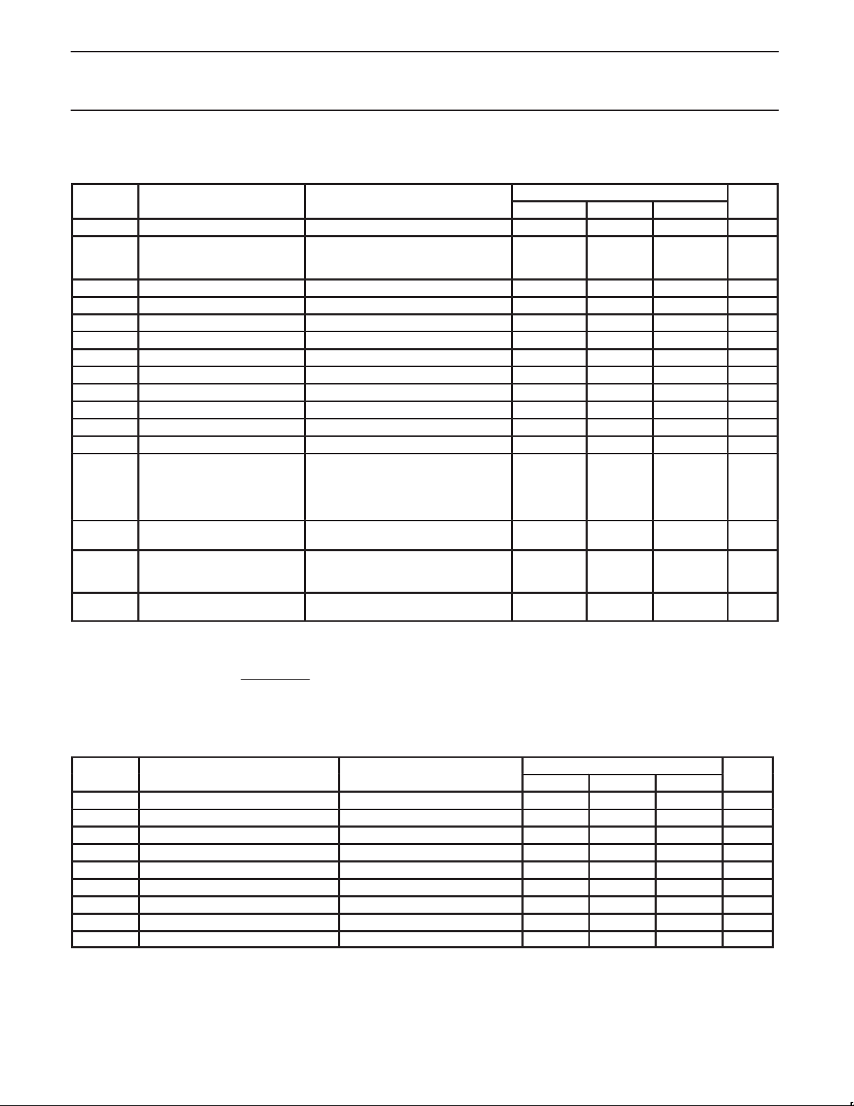
DC ELECTRICAL CHARACTERISTICS
VBB = 7.5 to 18 V; VCC = 4.5 to 5.5 V; TA = –40 to +85°C.
LIMITS
MIN TYP MAX
V
BB
I
IGN
I
CC
V
OH
V
OL
VOL Status ST, IOL = 2.5 mA 0.8 V
IOH Status ST, VO (ST) = V
V
IH
V
IL
I
IH
I
IL
A
CC
I
SD
V
DRIVE
R
LMIN
V
BIAS
NOTE:
1. V
DRIVE
2. In reference to nominal values in Figure 4. (Based on 7+ bit DAC).
3.
Output Angle (0) + tan
Analog supply voltage 7.5 18 V
Analog supply current
= 18 V no load
IGN
VBB = 18 V with load
RC1 = RC2 = R
LMIN
30
235
V
Logic supply current VCC = 5.5 V 1.0 mA
Output high voltage Data out IOH = 800 µA VCC – 0.8
Output low voltage Data out IOL = 1.5 mA 0.4 V
25 µA
CC
1 µA
1 µA
±1 Degree
Input high voltage CS, S
Input low voltage CS, S
Input high current CS, S
Input low current CS, S
Output function accuracy
2
, DATAIN, VIN = 0.7 x V
CLK
, DATAIN, VIN = 0.3 x V
CLK
RC1 = RC2 = R
CC
, DATAIN, OE 0.7 x V
CLK
, DATAIN, OE 0.3 x V
CLK
CC
CC
LMIN
CC
C1+, C1–, C2+, C2–, COM
Output shut-down current
Differential coil drive voltage
Minimum load resistance
Bias voltage
3
1
I
SINK
I
SOURCEVBB
VBB = V
BB (MAX)
VBB = V
BB (MIN)
= V
BB (MAX)
VBB = V
BB (MIN)
VBB = V
BB (MAX)
RL = R
L (MIN)
TA = 85°C
TA = 25°C
TA = –40°C
IOB (Source or Sink)
RL = R
L (MIN)
85
43
85
43
0.7 x V
215
171
138
0.475 x V
BB
BB
500
300
500
300
0.8 x V
0.525 x V
BB
BB
is the maximum voltage that is applied across the coil, it is equal to (C1+) – (C1–) or (C2+) – (C2–).
(C ))–(C–)
–1
ƪ
V
BB
–V
ƫ
BIAS
mA
V
V
mA
mA
mA
mA
V
Ω
Ω
Ω
V
AC ELECTRICAL CHARACTERISTICS
VDD = 7.5 to 18 V; VCC = 4.5 to 5.5 V; TA = –40 to +85°C
LIMITS
MIN TYP MAX
FS
CLK
TS
CLKH
TS
CLKL
TRO Output rise time DO 0.75 to VCC –1.2 V, CL = 90 pF 75 ns
TFO Output fall time DO VCC –1.2 V to 0.75, CL = 90 pF 75 ns
TSU DI set-up time 75 ns
THI DI hold time 75 ns
T
CSH
T
CSL
1999 Sep 20
Input frequency 1.60 MHz
S
high time 175 ns
CLK
S
low time VCC = 5.5 V 175 ns
CLK
Time before first S
Time after last S
rising edge 75 ns
CLK
falling edge 75 ns
CLK
5
Page 6
Philips Semiconductors Product specification
SA5777ADual air-core gauge driver
FUNCTIONAL DESCRIPTION
The SA5777A dual air-core gauge driver logic Block Diagram shows
the two 10-bit input shift registers and two 9-bit parallel latches, and
two 7+-bit DACs. The MSB is a dummy bit required for compatibility
with the SA5775A. The DACs generate output voltages that are
offset within the supply rails to give the output buffers enough
headroom to operate. With a 14 V supply, the typical output swing is
from 1 V to 11.5 V. The MUX generates the two required quadrants
by switching the 56° data from the DAC to the appropriate output
buffer . The output buffers provide the necessary current to drive the
air-core gauge. The output buffers are always connected to the
coils and can sink and source sufficient current so that inductive
kickback is eliminated during normal operation.
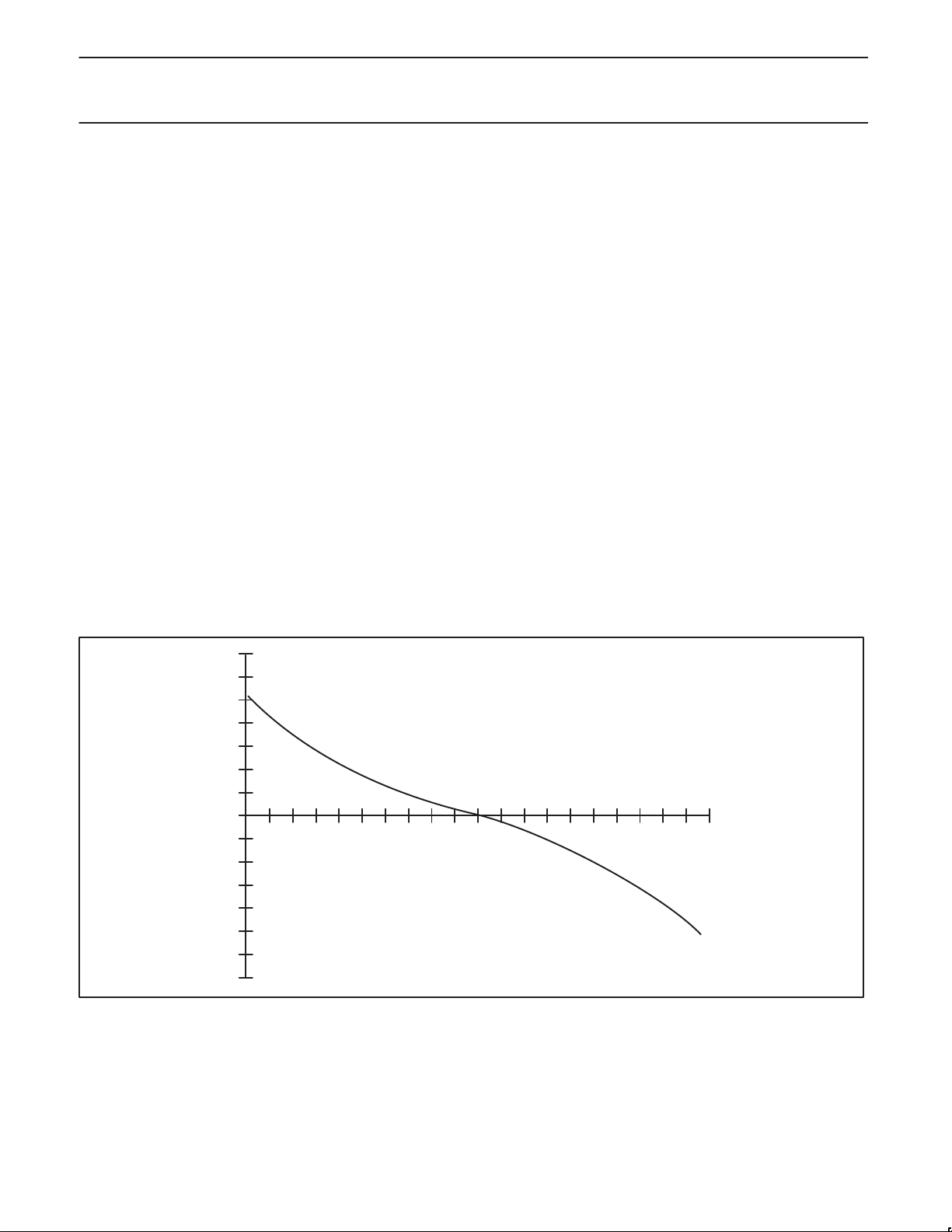
The primary function of the SA5777A IC is to generate the transfer
function that maps an input code into the correct voltages for linearly
controlling the coils of an air-core gauge display (Figure 3). The
SA5777A has been implemented using the tangent drive algorithm.
Therefore, one coil on each meter will be driven with an output
approximating the tangent function, the other coils will be biased at
1/2 V
. The internal DAC is designed to operate over a 7+ bit (56°)
BB
data range. An extended range can be achieved by changing the
relationship between the bias coil and the driver coil. As the current
through the bias coil is reduced, the full scale deflection is
increased. Theoretically, this deflection could approach 180°, but
practical limitations of accuracy, resolution, and torque restrict the
full scale range to approximately 112° (Figure 4). This full scale
range corresponds to a bias coil voltage of 0.5 x V
tangent voltage of 0.744 x V
. The DAC has been tailored to
BB
and a full scale
BB
maintain the meter accuracy at this maximum deflection. The 0.5 x
bias coil voltage is obtained by connecting the bias coils of the
V
BB
two meters in series across V
. This gives bias stability over
BB
temperature. The internal bias generator is used to offset any
inaccuracies due to meter mismatches. This circuit receives
commands via an internal serial data interface port which is SPI
compatible. These parts can be serially cascaded with other
SA5777A ICs and/or SA5775A ICs to interface signals in multi-chip
systems. The SA5777A has a typical resolution of 0.35° over a full
scale deflection of approximately 112° and is guaranteed to be
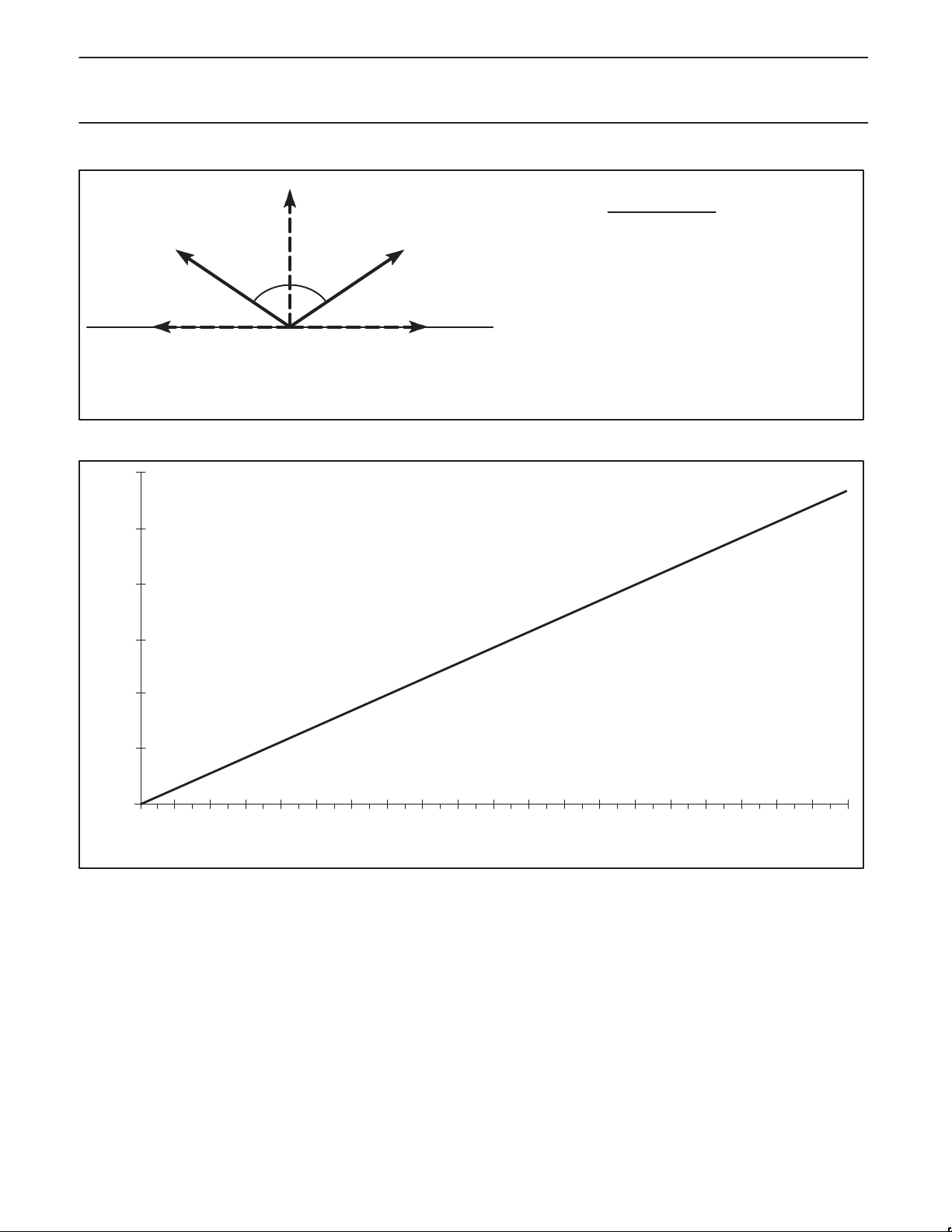
monotonic. The input data is directly proportional to the displayed
angle in degrees (Figure NO TAG). Input code 0 gives an output
angle of 0°, code 319 (decimal) will generate a full scale output of
112.15 °. Codes higher than decimal 319 will not be loaded into the
DAC latches and will leave the coil output buffers unchanged.
However, codes greater than 319 can be shifted through the
SA5777A intact if other parts are cascaded. The SA5777A is
capable of sourcing and sinking up to 100mA per differential driver
to control either one or two air-core gauge displays directly.
On-chip overcurrent and thermal shut-down logic prevents the chip
from overheating due to high current fault conditions. When a
shut-down condition is detected, the protection circuit disables the
coil output buffers (i.e., C1+, C1–, C2+, C2–, COM). The coil output
buffers remain in this condition until the first falling edge of CS that
occurs after the die temperature has decreased to about 140°C or
the overcurrent condition has been removed. During shut-down, the
digital portion of this IC continues to operate normally.
C+ – C– (VOLTS)
–10.00
–12.00
–14.00
14.00
12.00
10.00
8.00
6.00
4.00
2.00
0.00
–2.00
–4.00
–6.00
–8.00
31 63 95 127 159 191 223 255 287 319
INPUT CODE
SL00462
Figure 3. Typical output voltage vs input code (VBB = 14 V)
1999 Sep 20
6
Page 7
Philips Semiconductors Product specification
SA5777ADual air-core gauge driver
–0.744 x V
120
100
80
0.5 x V
BB
+56°–56°
BB
TOTAL SPAN = 112.15° STEP SIZE = 0.35°
0.744 x V
BB
Figure 4. Total span
ASSUMING CODE 0 IS 0°:
CODE
31
63
95
127
159
191
223
255
287
319
IDEAL ANGLE(DEGREE)=CODE/319*2* ArcTan (0.744/0.5)–ArcTan(0.744/0.5)
POSITION
0
–56.097
–45.194
–33.940
–22.685
–11.430
–0.176
11.079
22.333
33.588
44.843
56.097
SL00463
60
ANGLE (DEGREES)
40
20
0
01531 637995111127143
Figure 5. Meter position (degrees) vs input code
159 175 191 207 223 239 255 271 287 30341
INPUT CODE
319
SL00464
1999 Sep 20
7
Page 8
Philips Semiconductors Product specification
SA5777ADual air-core gauge driver
CS
20 S
CYCLES
CLK
TSU
THI
TS
80%
20%
CLKL
TS
CLKH
TC
SL
S
DATA
CLK
FS
T
CSH
1 2 19 20
IN
D19 D18 D1 D0
CLK
DATA
OUT
D0 D1 D2 D3 D4 D5 D6 D7 D8 D9 D10 D11 D12 D13 D14 D15 D16 D17 D18 D19
LSB
*DO IS THE PREVIOUSLY LOADED DATA WORD
D19* D18* D1* D0*
TFO TRO
GAUGE 2 GAUGE 1
MSB LSB MSB
SL00465
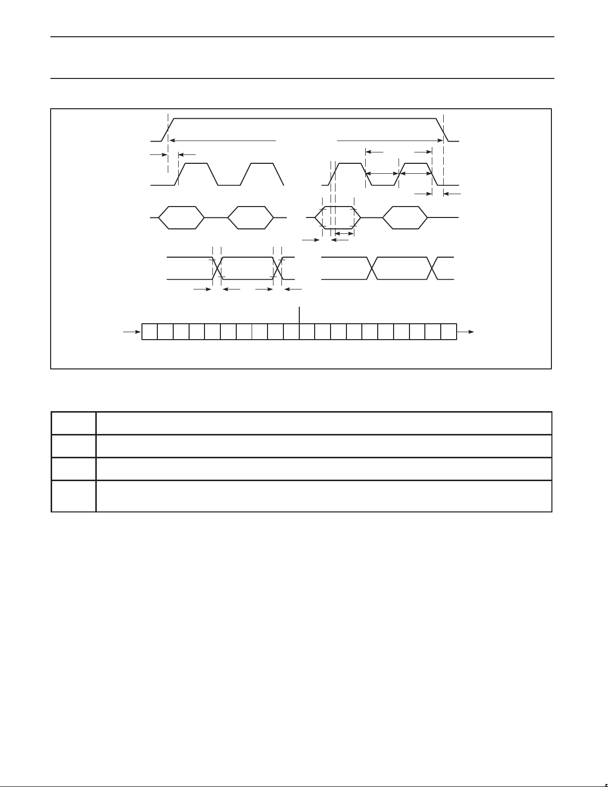
Figure 6. Serial interface timing
Serial Interface
The SA5777A is controlled through a serial interface with the following control functions (reference Figure 6):
S
CLK
Serial input clock. When CS is high, the rising edge of S
the data out of DATA
OUT
.
CS Active high chip select. Enables the SA5777A to receive serial input data. The falling edge of CS loads a new 20-bit data word
into the internal DAC registers which updates the tangent coil output buffers (C1+, C1–, C2+, C2–).
DATA
DATA
Serial data input. The data at this pin is shifted into the internal shift register on the rising edge of S
IN
first, gauge 1 first.
Serial data output. This pin is the output of the internal shift register. The data output on this pin is the input data from DATA
OUT
pin delayed by 20 clock cycles. This pin can be used to cascade several SA5777As with one CS line to load all of the
SA5777As concurrently.
Power Moding
The SA5777A has a power-on reset capability. On the rising edge
of V
, the internal latches and registers are set to zero and the coil
CC
output buffers (C1+, C1–, C2+, C2–, COM) are disabled.
shifts a new data bit into the SA5777A and the falling edge shifts
CLK
. Data is shifted in MSB
CLK
4. Due to excessive power dissipation (i.e., thermal shut-down).
The die temperature must go below 140°C before a falling edge
on the CS pin will clear this fault condition and allow the coil
outputs to go active.
IN
Coil Output Buffer Control
The coil buffers (C1+, C1–, C2+, C2–, COM) are disabled:
1. With the rising edge of V
2. When OE is taken low or held low. The data registers for the
outputs can still be updated while OE is low. When OE is taken
high, the current output data value is displayed. A falling edge
on CS will be required to activate the outputs if a fault condition
has occurred prior to the OE going high.
3. Due to an overcurrent condition on either of the coil output
buffers. The coil output buffers will be enabled after the next CS
high-to-low transition; assuming OE is high. If the overcurrent
condition has not been removed, the outputs will immediately
return to their disabled condition. The ST pin will indicate status
of the coil outputs.
1999 Sep 20
(power-on reset).
CC
Application Notes
The air-core gauge is constructed of two coils would on a cavity at
90° to each other. Inside the cavity there is a disk which is
magnetized on its diameter. The currents through the coils generate
a resultant magnetic vector that causes the magnetic disc to move
until the magnetic fields are aligned. If the ratio of the currents in the
two coils follows the tangent function, then the transfer characteristic
relating the input data to output angle is linear.
Maximum current is when output is at zero and full scale degrees,
T
= –40°C, and RL = 180.
A
Copper wire has a typical temperature coefficient of 0.4%/C
8
Page 9
Philips Semiconductors Product specification
SA5777ADual air–core gauge driver
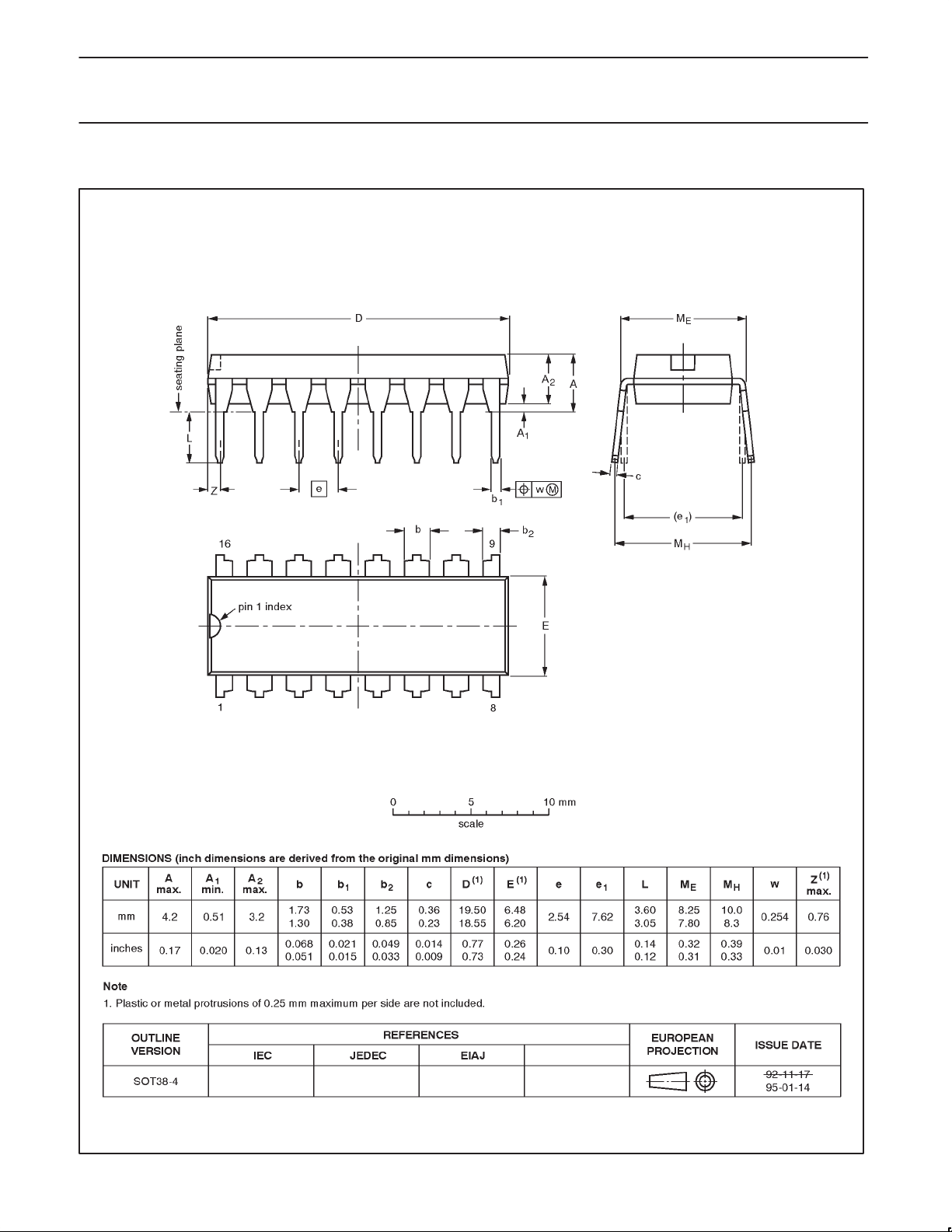
DIP16: plastic dual in-line package; 16 leads (300 mil) SOT38-4
1999 Sep 20
9
Page 10
Philips Semiconductors Product specification
SA5777ADual air–core gauge driver
SO28: plastic small outline package; 28 leads; body width 7.5mm SOT136-1
1999 Sep 20
10
Page 11

Philips Semiconductors Product specification
SA5777ADual air–core gauge driver
NOTES
1999 Sep 20
11
Page 12
Philips Semiconductors Product specification
SA5777ADual air–core gauge driver
Data sheet status
Data sheet
status
Objective
specification
Preliminary
specification
Product
specification
Product
status
Development
Qualification
Production
Definition
This data sheet contains the design target or goal specifications for product development.
Specification may change in any manner without notice.
This data sheet contains preliminary data, and supplementary data will be published at a later date.
Philips Semiconductors reserves the right to make changes at any time without notice in order to
improve design and supply the best possible product.
This data sheet contains final specifications. Philips Semiconductors reserves the right to make
changes at any time without notice in order to improve design and supply the best possible product.
[1]
[1] Please consult the most recently issued datasheet before initiating or completing a design.
Definitions
Short-form specification — The data in a short-form specification is extracted from a full data sheet with the same type number and title. For
detailed information see the relevant data sheet or data handbook.
Limiting values definition — Limiting values given are in accordance with the Absolute Maximum Rating System (IEC 134). Stress above one
or more of the limiting values may cause permanent damage to the device. These are stress ratings only and operation of the device at these or
at any other conditions above those given in the Characteristics sections of the specification is not implied. Exposure to limiting values for extended
periods may affect device reliability.
Application information — Applications that are described herein for any of these products are for illustrative purposes only. Philips
Semiconductors make no representation or warranty that such applications will be suitable for the specified use without further testing or
modification.
Disclaimers
Life support — These products are not designed for use in life support appliances, devices or systems where malfunction of these products can
reasonably be expected to result in personal injury . Philips Semiconductors customers using or selling these products for use in such applications
do so at their own risk and agree to fully indemnify Philips Semiconductors for any damages resulting from such application.
Right to make changes — Philips Semiconductors reserves the right to make changes, without notice, in the products, including circuits, standard
cells, and/or software, described or contained herein in order to improve design and/or performance. Philips Semiconductors assumes no
responsibility or liability for the use of any of these products, conveys no license or title under any patent, copyright, or mask work right to these
products, and makes no representations or warranties that these products are free from patent, copyright, or mask work right infringement, unless
otherwise specified.
Philips Semiconductors
811 East Arques Avenue
P.O. Box 3409
Sunnyvale, California 94088–3409
Telephone 800-234-7381
Copyright Philips Electronics North America Corporation 1999
All rights reserved. Printed in U.S.A.
Date of release: 09-99
Document order number: 9397 750 06444
1999 Sep 20
12
 Loading...