

Page 1

NTE995 & NTE995M
Integrated Circuit
Frequency–to–Voltage Converter
Description:
The NTE995 (14–Lead DIP) and NTE995M (8–Lead DIP) are monolithic frequency to voltage converters with a high gain OP amp/comparator designed to operate a relay, lamp, or other load when
the input frequency reaches or exceeds a selected rate. The tachometer uses a charge pump technique and offers frequency doubling for low ripple, full input protection, and its output swings to GND
for a zero frequency input.
Advantages:
D Output Swing to GND for Zero Frequency Input
D Easy to Use: V
D Only One RC Network Provides Frequency Doubling
D Zener Regulator On Chip Allows Accurate and Stable Frequency to Voltage or Current Conversion
Features:
D Ground Referenced Tachometer Input Interfaces Directly with Variable Reluctance Magnetic
Pickups
D OP Amp/Comparator has Floating Transistor Output
D 50mA Sink or Source to Operate Relays, Solenoids, Meters, or LEDs
D Frequency Doubling for Low Ripple
D Tachometer has Built–In Hysteresis with Either Differential Input or Ground Referenced Input
D Built–In Zener Diode
D ±0.3% Linearity Typical
D Ground Referenced Tachometer is Fully Protected from damage Due to Swings Above V
and Below GND
= fIN x VCC x R1 x C1
OUT
CC
Applications:
D Over/Under Speed Sensing
D Frequency to Voltage Conversion (Tachometer)
D Speedometers
D Breaker Point Dwell Meters
D Hand–Held Tachometer
D Speed Governors
D Cruise Control
D Automotive Door Lock Control
D Clutch Control
D Horn Control
D Touch or Sound Switches
Page 2
Absolute Maximum Ratings:
Supply Voltage, V
CC
Supply Current (Zener Options) 25mA. . . . . . . . . . . . . . . . . . . . . . . . . . . . . . . . . . . . . . . . . . . . . . . . . . . .
Collector Voltage 28V. . . . . . . . . . . . . . . . . . . . . . . . . . . . . . . . . . . . . . . . . . . . . . . . . . . . . . . . . . . . . . . . . . .
Differential Input Voltage
Tachometer 28V. . . . . . . . . . . . . . . . . . . . . . . . . . . . . . . . . . . . . . . . . . . . . . . . . . . . . . . . . . . . . . . . . .
OP Amp/Comparator 28V. . . . . . . . . . . . . . . . . . . . . . . . . . . . . . . . . . . . . . . . . . . . . . . . . . . . . . . . .
Input Voltage Range
Tachometer
NTE995M ±28V. . . . . . . . . . . . . . . . . . . . . . . . . . . . . . . . . . . . . . . . . . . . . . . . . . . . . . . . . . . . . . .
NTE955 0.0V to +28V. . . . . . . . . . . . . . . . . . . . . . . . . . . . . . . . . . . . . . . . . . . . . . . . . . . . . . . . . .
OP Amp/Comparator 0.0V to +28V. . . . . . . . . . . . . . . . . . . . . . . . . . . . . . . . . . . . . . . . . . . . . . . . .
Power Dissipation (Note 1), P
D
NTE995M 1200mW. . . . . . . . . . . . . . . . . . . . . . . . . . . . . . . . . . . . . . . . . . . . . . . . . . . . . . . . . . . . . .
NTE995 1580mW. . . . . . . . . . . . . . . . . . . . . . . . . . . . . . . . . . . . . . . . . . . . . . . . . . . . . . . . . . . . . . . .
Operating Temperature Range, T
Storage Temperature Range, T
Lead Temperature, T
L
stg
opr
–40° to +85°C. . . . . . . . . . . . . . . . . . . . . . . . . . . . . . . . . . . . . . . . .
–65° to +150°C. . . . . . . . . . . . . . . . . . . . . . . . . . . . . . . . . . . . . . . . . .
NTE995, NTE995M (During Soldering, 10sec) +260°C. . . . . . . . . . . . . . . . . . . . . . . . . . . . . . . .
NTE995M
(Vapor Phase, 60sec) +215°C. . . . . . . . . . . . . . . . . . . . . . . . . . . . . . . . . . . . . . . . . . . . . . . . . . .
(Infrared, 15sec) +220°C. . . . . . . . . . . . . . . . . . . . . . . . . . . . . . . . . . . . . . . . . . . . . . . . . . . . . . .
28V. . . . . . . . . . . . . . . . . . . . . . . . . . . . . . . . . . . . . . . . . . . . . . . . . . . . . . . . . . . . . . . .
Note 1. For operation in ambient temperatures above 25°C, the device must be derated based on
a +150°C maximum junction temperature and a thermal resistance of +101°C/W junction to
ambient for the NTE995M, and +79°C/W junction to ambient for the NTE995.
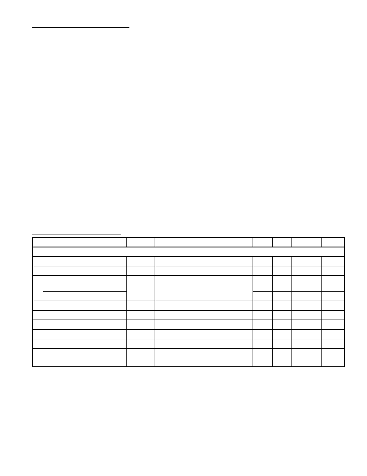
Electrical Characteristics:
Parameter Symbol Test Conditions Min Typ Max Unit
Tachometer
Input Thresholds VIN = 250mV
Hysteresis VIN = 250mV
Offset Voltage
NTE995
NTE995M – 5.0 15 mV
Input Bias Current VIN = ±50mV – 0.1 1.0 µA
Output Voltage (High Level, Pin2) V
Output Voltage (Low Level, Pin2) V
Output Current I2, I
Leakage Current I
Gain Constant K Note 3 0.9 1.0 1.1
Linearity fIN = 1kHz, 5kHz, 10kHz, Note 5 –1.0 0.3 +1.0 %
(VCC = 12V, TA = +25°C unless otherwise specified)
@ 1kHz, Note 2 ±10 ±25 ±40 mV
P–P
@ 1kHz, Note 2 – 30 – mV
P–P
OH
OL
3
VIN = 250mV
VIN = +125mV, Note 3 – 8.3 – V
VIN = –125mV, Note 3 – 2.3 – V
V2 = V3 = 6V, Note 4 140 180 240 µA
3
I2 = 0, V3 = 0 – – 0.1 µA
@ 1kHz, Note 2
P–P
– 3.5 10 mV
Note 2. Hysteresis is the sum + VTH – (–VTH), offset voltage is their difference.
Note 3. V
is equal to 3/4 x VCC – 1 VBE, VOL is equal to 1/4 x VCC – 1 VBE therefore VOH – VOL = VCC/2.
OH
The difference, V
– VOL, and the mirror gain, I2/I3, are two factors that cause the tachometer
OH
gain constant to vary from 1.0.
Note 4. Be sure when choosing the time constant R1 x C1 that R1 is such that the maximum antici-
pated output voltage at Pin3 can be reached with I
x R1. The maximum value for R1 is lim-
3
ited by the output resistance of Pin3 which is greater than 10MΩ typically.
Note 5. Nonlinearity is defined as the deviation of V
defined by the V
@ 1kHz and V
OUT
@ 10kHz. C1 = 1000pF, R1 = 68k and C2 = 0.22mFd.
OUT
(@ Pin3) for fIN = 5kHz from a straight line
OUT
Page 3

Electrical Characteristics (Cont’d): (VCC = 12V, TA = +25°C unless otherwise specified)
Parameter Symbol Test Conditions Min Typ Max Unit
OP Amp/Comparator
V
OS
I
BIAS
Input Common–Mode Voltage 0 – VCC–1.5V V
Voltage Gain – 200 – V/mV
Output Sink Current VC = 1.0 40 50 – mA
Output Source Current VE = VCC – 2.0 – 10 – mA
Saturation Voltage I
Zener Regulator
Regulator Voltage R
Series Resistance – 10.5 15.0 Ω
Temperature Stability – +1 – mV/°C
Total Supply Current – 3.8 6.0 mA
VIN = 6V – 3 10 mV
VIN = 6V – 50 500 nA
= 5mA – 0.1 0.5 V
SINK
I
= 20mA – – 1.0 V
SINK
I
= 50mA – 1.0 1.5 V
SINK
= 470Ω – 7.56 – V
DROP
NTE995 NTE995M
+ Comparator N.C.
Charge Pump Cap
Charge Pump Out
+ Op Amp In
Output Emitter
N.C.
N.C.
1
2
3
4
5
6
7
Pin Connection Diagram
14
N.C.
13
GND
12
11
– Comparator In
– Op Amp In
10
9
Vcc
8
Output Collector
+ Comparator In
Charge Pump Cap
Charge Pump
Output
Emitter Output
1
2
3
4
GND/
8
Frequency Input
7
– Op Amp In
Vcc
6
5 Collector Output
Page 4

NTE995
14 8
17
.785 (19.95)
Max
.200 (5.08)
Max
.100 (2.45) .099 (2.5) Min
.600 (15.24)
NTE995M
85
.256 (6.52) Max
.300
(7.62)
14
.393 (10.0)
Max
.150
(3.81)
.300 (7.62)
.300
(7.62)
.070 (1.77) Min.100 (2.54)
 Loading...