

Page 1

NTE99
Silicon NPN Transistor
w
Darlington
Description:
The NTE99 is a silicon NPN Darlington transistor in a TO3 type package designed for high–voltage,
high–speed, power switching in inductive circuits where fall time is critical. This device is particularly
suited for line–operated switchmode applications.
Applications:
D Switching Regulators
D Motor Controls
D Inverters
D Solenoid and Relay Drivers
Features:
D Fast Turn–Off Times:
1.0µs (max) Inductive Crossover Time – 20 Amps
2.5µs (max) Inductive Storage Time – 20 Amps
D Operating Temperature Range: –65° to +200°C
/Base–Emitter Speed–up Diode
Absolute Maximum Ratings:
Collector–Emitter Voltage, V
Collector–Emitter Voltage, V
Emitter–Base Voltage, V
Collector Current, I
C
CEO
CEV
EB
Continuous 50A. . . . . . . . . . . . . . . . . . . . . . . . . . . . . . . . . . . . . . . . . . . . . . . . . . . . . . . . . . . . . . . . . .
Peak (Note 1) 75A. . . . . . . . . . . . . . . . . . . . . . . . . . . . . . . . . . . . . . . . . . . . . . . . . . . . . . . . . . . . . . . .
Base Current, I
B
Continuous 10A. . . . . . . . . . . . . . . . . . . . . . . . . . . . . . . . . . . . . . . . . . . . . . . . . . . . . . . . . . . . . . . . . .
Peak (Note 1) 15A. . . . . . . . . . . . . . . . . . . . . . . . . . . . . . . . . . . . . . . . . . . . . . . . . . . . . . . . . . . . . . . .
Total Power Dissipation, P
D
TC = +25°C 250W. . . . . . . . . . . . . . . . . . . . . . . . . . . . . . . . . . . . . . . . . . . . . . . . . . . . . . . . . . . . . . . .
Derate Above 25°C 1.43W/°C. . . . . . . . . . . . . . . . . . . . . . . . . . . . . . . . . . . . . . . . . . . . . . . . . . . . . .
T
= +100°C 143W. . . . . . . . . . . . . . . . . . . . . . . . . . . . . . . . . . . . . . . . . . . . . . . . . . . . . . . . . . . . . . .
C
Operating Junction Temperature Range, T
Storage Temperature Range, T
stg
Thermal Resistance, Junction–to–Case, R
J
thJC
Maximum Lead Temperature (During Soldering, 1/8” from case for 5sec), T
Note 1. Pulse Test: Pulse Width = 5ms, Duty Cycle ≤ 10%.
400V. . . . . . . . . . . . . . . . . . . . . . . . . . . . . . . . . . . . . . . . . . . . . . . . . . . . .
600V. . . . . . . . . . . . . . . . . . . . . . . . . . . . . . . . . . . . . . . . . . . . . . . . . . . . .
8V. . . . . . . . . . . . . . . . . . . . . . . . . . . . . . . . . . . . . . . . . . . . . . . . . . . . . . . . . . .
–65° to +200°C. . . . . . . . . . . . . . . . . . . . . . . . . . . . . . . . . .
–65° to +200°C. . . . . . . . . . . . . . . . . . . . . . . . . . . . . . . . . . . . . . . . . .
0.7°C/W. . . . . . . . . . . . . . . . . . . . . . . . . . . . . . . . . . . . .
L
+275°C. . . . . . . . . . . .
Page 2
Electrical Characteristics: (TC = +25°C unless otherwise specified)
µ
Parameter Symbol Test Conditions Min Typ Max Unit
OFF Characteristics (Note 2)
Collector–Emitter Sustaining Voltage V
Collector Cutoff Current I
Emitter Cutoff Current I
CEO(sus)IC
CEV
EBO
ON Characteristics (Note 2)
DC Current Gain h
Collector–Emitter Saturation Voltage V
Base–Emitter Saturation Voltage V
CE(sat)IC
BE(sat)IC
Diode Forward Voltage V
Dynamic Characteristic
Output Capacitance C
Switching Characteristics
Resistive Load
Delay Time t
Rise Time t
Storage Time t
Fall Time t
Inductive Load, Clamped
FE
ob
d
s
= 100mA, IB = 0, V
V
= 600V, V
CEV
BE(off)
= 400V 400 – – V
clamp
= 1.5V – – 0.25 mA
VBE = 2V, IC = 0 – – 350 mA
IC = 20A, VCE = 5V 25 – –
IC = 40A, VCE = 5V 10 – –
= 20A, IB = 1A – – 2.2 V
IC = 50A, IB = 10A – – 5.0 V
= 20A, IB = 1A – – 2.75 V
IF = 20A, Note 3 – 2.5 5.0 V
f
VCB = 10V, IE = 0, f
VCC = 250V, IC = 20A,
IB1 = 1A, V
r
tp = 25µs, Duty Cycle ≤ 2%
t = 25
BE(off)
s, Duty Cycle ≤ 2%
= 100kHz – – 750 pF
test
– 0.14 0.3 µs
= 5V,
– 0.3 1.0 µs
– 0.8 2.5 µs
f
– 0.3 1.0 µs
Storage Time t
Crossover Time t
sv
IC = 20A(pk), V
IB1 = 1A, V
c
BE(off)
clamp
= 5V
= 250V,
– 1.0 2.5 µs
– 0.36 1.0 µs
Note 2. Pulse Test: Pulse Widtg = 300µs, Duty Cycle ≤ 2%.
Note 3. The internal Collector–to–Emitter diode can eliminate the need for an external diode to
clamp inductive loads. Tests have shown that the Forward Recovery Voltage (V
) of this
f
diode is comparable to that of typical fast recovery rectifiers.
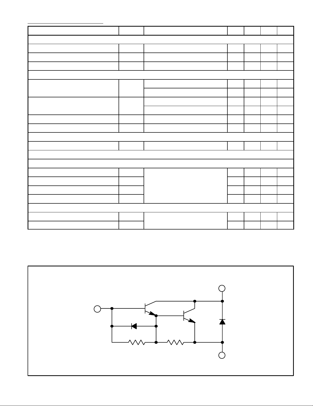
Circuit Outline
C
B
[ 50 [ 8
E
Page 3

.135 (3.45) Max
.350 (8.89)
.215 (5.45)
.430
(10.92)
Emitter
.875 (22.2)
Dia Max
Seating
Plane
.040 (1.02).312 (7.93) Min
1.187 (30.16)
.665
(16.9)
.156 (3.96) Dia
(2 Holes)
.188 (4.8) R Max
.525 (13.35) R Max
Collector/CaseBase
 Loading...