

Page 1
NTE989
Integrated Circuit
General Purpose Phase Lock Loop (PLL)
Description:
The NTE989 is a general purpose Phase Locked Loop (PLL) in a 14–Lead DIP type package containing a stable, highly linear voltage controlled oscillator for low distortion FM demodulation, and a
double balanced phase detector with good carrier suppression. The VCO frequency is set with an
external resistor and capacitor, and tuning range of 10:1 can be obtained with the same capacitor.
The characteristics of the closed loop system–bandwidth, response speed, capture and pull in range–
may be adjusted over a wide range with an external resistor and capacitor. The loop may be broken
between the VCO and the phase detector for insertion of a digital frequency divider to obtain frequency multiplication.
Features:
D 200ppm/°C frequency stability of the VCO
D Power supply range of ±5 to ±12 volts with 100ppm/% typical
D 0.2% linearity of demodulated output
D Linear triangle wave with in phase zero crossings available
D TTL and DTL compatible phase detector input and square wave output
D Adjustable hold in range from ±1% to > ±60%
Applications:
D Data and tape synchronization
D Modems
D FSK demodulation
D FM demodulation
D Frequency synthesizer
D Tone decoding
Absolute Maximum Ratings:
Supply Voltage ±12V. . . . . . . . . . . . . . . . . . . . . . . . . . . . . . . . . . . . . . . . . . . . . . . . . . . . . . . . . . . . . . . . . . . .
Power Dissipation (Note 1) 300mW. . . . . . . . . . . . . . . . . . . . . . . . . . . . . . . . . . . . . . . . . . . . . . . . . . . . . .
Differential Input Voltage ±1V. . . . . . . . . . . . . . . . . . . . . . . . . . . . . . . . . . . . . . . . . . . . . . . . . . . . . . . . . . . .
Operating Temperature Range 0°C to +70°C. . . . . . . . . . . . . . . . . . . . . . . . . . . . . . . . . . . . . . . . . . . . . . .
Storage Temperature Range –65°C to +150°C. . . . . . . . . . . . . . . . . . . . . . . . . . . . . . . . . . . . . . . . . . . . .
Lead Temperature (Soldering, 10 sec) +300°C. . . . . . . . . . . . . . . . . . . . . . . . . . . . . . . . . . . . . . . . . . . . .
D Frequency multiplication and division
D SCA demodulators
D Telemetry receivers
D Signal regeneration
D Coherent demodulators
Note 1. The maximum junction temperature of the NTE989 is 100°C. Thermal resistance for this
device is 100°C/W.
Page 2
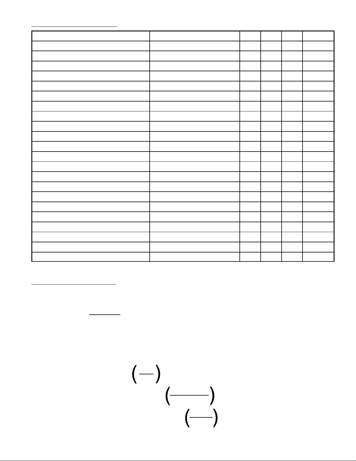
Electrical Characteristics: (TA = +25°C, VC = ±6V unless otherwise specified)
Parameter Conditions Min Typ Max Unit
Power Supply Current – 8.0 12.5 mA
Input Impedance (Pins 2,3) –4V < V2, V3 < 0V – 5 – kΩ
VCO Maximum Operating Frequency Co = 2.7pF 250 500 – kHz
Operating Frequency Temperature Coefficient – –200 500 ppm/°C
Frequency Drift with Supply Voltage – 0.05 0.2 %/V
Triangle Wave Output Voltage 2 2.4 3 V
Triangle Wave Output Linearity – 0.5 1 %
Square Wave Output Level 4.7 5.4 – V
Output Impedance (Pin 4) – 5 – kΩ
Square Wave Duty Cycle 40 50 60 %
Square Wave Rise Time – 20 – ns
Square Wave Fall Time – 50 – ns
Output Current Sink (Pin 4) 0.6 1 – mA
VCO Sensitivity fo = 10kH
Demodulated Output Voltage (Pin 7) ±10% Frequency Deviation 200 300 400 mV
Total Harmonic Distortion ±10% Frequency Deviation – 0.2 1.5 %
Output Impedance (Pin 7) – 3.5 – kΩ
DC Level (Pin 7) 4.0 4.5 5.0 V
Output Offset Voltage |V7 – V6| – 50 200 mV
Temperature Drift of |V7 – V6| – 500 – µV/°C
AM Rejection – 40 – dB
Phase Detector Sensitivity K
D
Z
6000 6600 7200 HZ/V
0.55 .68 0.95 V/radian
p–p
p–p
pp
Applications Information:
In designing with phase locked loops the important parameters of interest are:
FREE RUNNING FREQUENCY
1
≅
f
o
3.7 R
0C0
LOOP GAIN:
The Loop Gain relates the amount of phase change between the input signal and the VCO signal for a shift in input signal frequency (assuming the loop remains in lock). In servo theory,
this is called the “velocity error coefficient”.
1
Loop gain = KoK
D
sec
radians/sec
Ko = oscillator sensitivity
volt
volts
KD = phase detector sensitivity
radian
Page 3

Applications Information (Cont’d):
LOOP GAIN (Cont’d):
The loop gain of the NTE989 is dependent on supply voltage, and may be found from:
K
oKD
33.6 f
=
V
o
c
fo = VCO frequency in H
Vc = total supply voltage to circuit
Loop gain may be reduced by connecting a resistor between Pin6 and Pin7; this reduces the
load impedance on the output amplifier and hence the loop gain.
HOLD IN RANGE:
The Hold In Range is the range of frequencies that the loop will remain in lock after initially being locked.
8 f
V
o
c
f
H
= ±
fo = free running frequency of VCO
V
= total supply voltage to the circuit
c
THE LOOP FILTER
In almost all applications, it will be desirable to filter the signal at the output of the phase detector (Pin7).
A simple lag filter may be used for wide closed loop bandwidth applications such as modulation
following where the frequency deviation of the carrier is fairly high (greater than 10%), or where
wideband modulating signals must be followed.
For narrow band applications where a narrow noise bandwidth is desired, such as applications
involving tracking a slowly varying carrier, a lead lag filter should be used. In general the damping factor for the loop becomes quite small resulting in large overshoot and possible instability
in the transient response of the loop.
Z
(–) V
CC
Input
Input
VCO Output
Phase Comparator
VCO Input
Pin Connection Diagram
1
2
3
4
5
6Reference Output
7
14
13
12
11
10
9
8
N.C.
N.C.
N.C.
N.C.
(+) V
CC
Timing Capacitor
Timing ResistorVCO Control Voltage
Page 4

14 8
17
.785 (19.95)
Max
.200 (5.08)
Max
.100 (2.45) .099 (2.5) Min
.600 (15.24)
.300 (7.62)
 Loading...