

Page 1

NTE980
Integrated Circuit
CMOS, Micropower Phase–Locked Loop (PLL)
Description:
The NTE980 CMOS Micropower Phase–Locked Loop (PLL) consists of a low–power, linear voltage–
controlled oscillator (VCO) and two different phase comparators having a common signal–input amplifier and a common comparator input in a 16–Lead type package. A 5.2V zener diode is provided
for supply regulation if necessary.
Features:
D Very Low Power Consumption: 70µW (Typ) @ VCO fo = 10kHz, VDD = 5V
D Operating Frequency Range up to 1.4MHz (Typ) @ V
D Low Frequency Drift: 0.04%/°C (Typ) @ V
DD
= 10V
D Choice of Two Phase Comparators:
Exclusive–OR Network (I)
DD
w
/Phase–Pulse Output for Lock Indication (II)
= 10V
Edge–Controlled Memory Network
D High VCO Linearity: < 1% (Typ) @ V
D VCO Inhibit Control for ON–OFF Keying and Ultra–Low Standby Power Consumption
D Source–Follower Output of VCO Control Input (Demod. Output)
D Zener Diode to Assist Supply Regulation
D Standardized, Symmetrical Output Characteristics
D 100% Tested for Quiescent Current at 20V
D 5V, 10V, and 15V Parametric Ratings
= 10V, RI = 5kΩ
DD
Applications:
D FM Demodulator and Modulator
D Frequency Synthesis and Multiplication
D Frequency Discriminator
D Signal Conditioning
D FSK – Modems
D Data Synchronization
D Voltage–to–Frequency Conversion
D Tone Decoding
Absolute Maximum Ratings:
DC Supply Voltage Range (Voltages referenced to VSS terminal), V
DD
–0.5 to +20V. . . . . . . . . . . .
Input Voltage Range, All Inputs –0.5 to V
DC Input Current, Any One Input ±10mA. . . . . . . . . . . . . . . . . . . . . . . . . . . . . . . . . . . . . . . . . . . . . . . . . .
Power Dissipation (T
T
= +60° to +85°C Derate Linearly at 12mW/°C to 200mW. . . . . . . . . . . . . . . . . . . . . . . . . . . .
A
Device Dissipation Per Output Transistor (T
Operating Temperature Range, T
Storage Temperature Range, T
Lead Temperature (During Soldering, 1/16” ±1/32” from case, 10sec Max), T
= –40° to +60°C), P
A
A
stg
D
= –40° to +85°C) 100mW. . . . . . . . . . . . . . . . . . . . . . .
A
–65° to +150°C. . . . . . . . . . . . . . . . . . . . . . . . . . . . . . . . . . . . . . . . . .
L
–40° to +85°C. . . . . . . . . . . . . . . . . . . . . . . . . . . . . . . . . . . . . . . . . . .
DD
500mW. . . . . . . . . . . . . . . . . . . . . . . . . . . . . . . . . . . . . . .
+265°C. . . . . . . . . . .
+0.5V. . . . . . . . . . . . . . . . . . . . . . . . . . . . . . . . . . . . . . . . . . .
Page 2
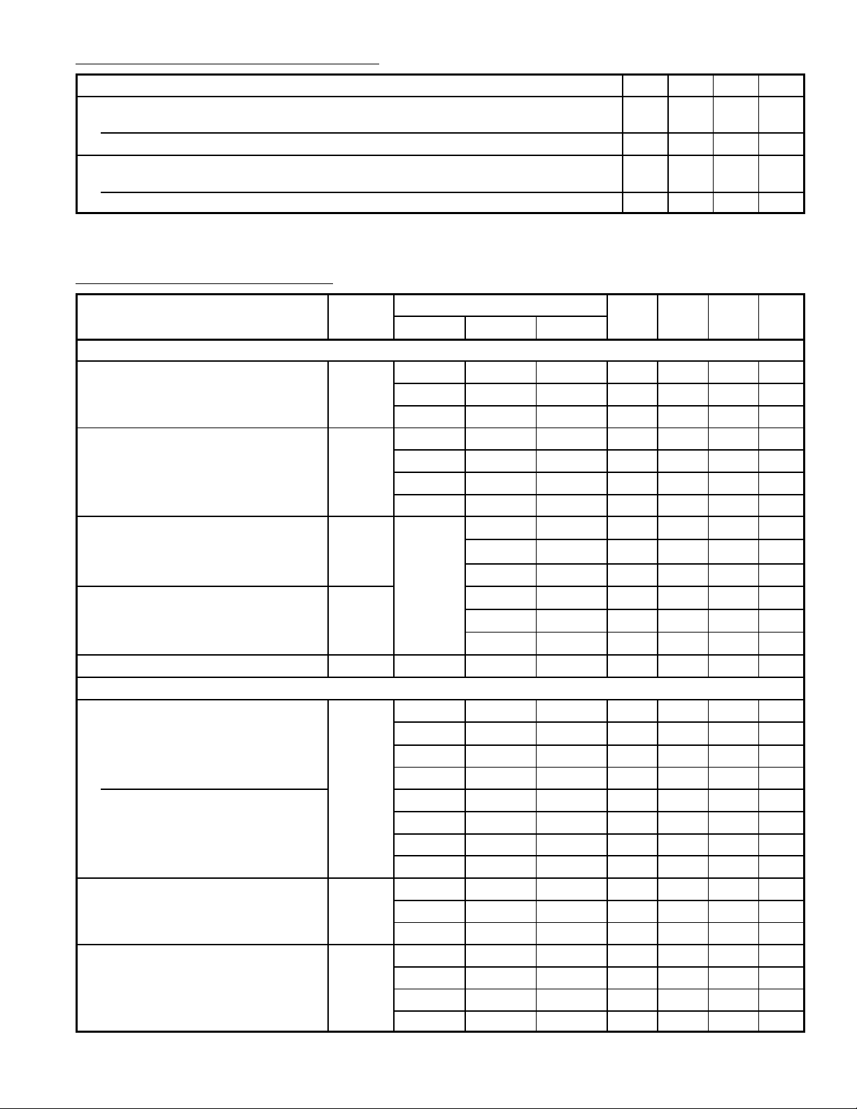
Recommended Operating Conditions: (TA = –40° to +85°C)
Parameter Min Typ Max Unit
Supply Voltage Range VCO Section:
As Fixed Oscillator
3 – 18 V
Phase–Lock–Loop Operation 5 – 18 V
Supply Voltage Range Phase Comparator Section:
Comparators
3 – 18 V
VCO Operation 5 – 18 V
Static Electrical Characteristics: (TA = +25°C unless otherwise specified)
Test Conditions
Parameter Symbol
V
O
VCO Section
Output Low (Sink) Current IOLMin 400mV 0V, 5V 5V 0.51 1.0 – mA
500mV 0V, 10V 10V 1.3 2.6 – mA
1.5V 0V, 15V 15V 3.4 6.8 – mA
Output High (Source) Current IOHMin 4.6V 0V, 5V 5V –0.51 –1.0 – mA
2.5V 0V, 5V 5V –1.6 –3.2 – mA
9.5V 0V, 10V 10V –1.3 –2.6 – mA
13.5V 0V, 15V 15V –3.4 –6.8 – mA
Output Voltage: Low–Level VOLMax
Pin4
driving
CMOS
CMOS
Output Voltage: High–Level VOHMax
e.g.
Pin3
Input Current IINMax – 0V, 18V 18V – ±10
Phase Comparator Section
Total Device Current
Pin14 = Open, Pin5 = V
DD
IDDMax – 0V, 5V 5V – 0.1 0.2 mA
– 0V, 10V 10V – 0.5 1.0 mA
– 0V, 15V 15V – 0.75 1.5 mA
– 0V, 20V 20V – 2.0 4.0 mA
Pin14 = VSS or VDD, Pin5 = V
DD
– 0V, 5V 5V – 10.0 20.0 µA
– 0V, 10V 10V – 20.0 40.0 µA
– 0V, 15V 15V – 40.0 80.0 µA
– 0V, 20V 20V – 80.0 160.0 µA
Output Low (Sink) Current IOLMin 400mV 0V, 5V 5V 0.51 1.0 – mA
500mV 0V, 10V 10V 1.3 2.6 – mA
1.5V 0V, 15V 15V 3.4 6.8 – mA
Output High (Source) Current IOHMin 4.6V 0V, 5V 5V –0.51 –1.0 – mA
2.5V 0V, 5V 5V –1.6 –3.2 – mA
9.5V 0V, 10V 10V –1.3 –2.6 – mA
13.5V 0V, 15V 15V –3.4 –6.8 – mA
V
IN
V
DD Min Typ Max Unit
0V, 5V 5V – 0 0.05 V
0V, 10V 10V
–
0 0.05 V
0V, 15V 15V – 0 0.05 V
0V, 5V 5V 4.95 5.0 – V
0V, 10V 10V 9.95 10.0 – V
0V, 15V 15V 14.95 15.0 – V
–5
±0.1 µA
Page 3

Static Electrical Characteristics (Cont’d): (TA = +25°C unless otherwise specified)
Test Conditions
Parameter Symbol
V
O
V
IN
V
DD Min Typ Max Unit
Phase Comparator Section (Cont’d)
DC Coupled Signal Input and
Comparator Input Voltage Sensitivity
Low Level
Low Level
VILMax 0.5V, 4.5V – 5V – – 1.5 V
1V, 9V – 10V – – 3.0 V
1.5V, 13.5V – 15V – – 4.0 V
High Level VIHMax 0.5V, 4.5V – 5V 3.5 – – V
1V, 9V – 10V 7.0 – – V
1.5V, 13.5V – 15V 11.0 – – V
Input Current (Except Pin14) IINMax – 0V, 18V 18V – ±10
3–State Leakage Current I
Max 0V, 18V 0V, 18V 18V – ±10
OUT
–5
–5
±0.1 µA
±0.1 µA
Electrical Characteristics: (TA = +25°C)
Test Conditions
Parameter Symbol
VCO Section
Operating Power
Dissipation R2 = ∞
Maximum Operating
P
f
max
fo = 10kHz, R1 = 1MΩ,
D
C1 = 50pF,
V
VCO =
VCOIN =
DD
2
R1 = 10kΩ 5V 0.3 0.6 – MHz
Frequency R2 = ∞,
VCO = V
VCOIN = V
DD
R1 = 5kΩ 5V 0.5 0.8 – MHz
Linearity VCOIN = 2.5V±0.3V R1 = 10kΩ 5V – 1.7 – %
VCOIN = 5.0V±1.0V R1 = 100kΩ 10V – 0.5 – %
VCOIN = 5.0V±2.5V R1 = 400kΩ 10V – 4.0 – %
VCOIN = 7.5V±0.3V R1 = 100kΩ 15V – 0.5 – %
VCOIN = 7.5V±5.0V R1 = 1MΩ 15V – 7.0 – %
f
Temperature–Frequency
= 0 5V – ±0.12 – %/°C
MIN
Stability:
No Frequency Offset
No Frequency Offset
Frequency Offset f
0 0 5V – ±0.09 – %/°C
MIN
Output Duty Cycle 5, 10, 15V – 50 – %
Output Transition Times t
THL
, t
TLH
V
DD Min Typ Max Unit
5V – 70 140 µW
10V – 800 1600 µW
15V – 3000 6000 µW
10V 0.6 1.2 – MHz
15V 0.8 1.6 – MHz
10V 1.0 1.4 – MHz
15V 1.4 2.4 – MHz
10V – ±0.04 – %/°C
15V – ±0.015 – %/°C
10V – ±0.07 – %/°C
15V – ±0.03 – %/°C
5V – 100 200 ns
10V – 50 100 ns
15V – 40 80 ns
Page 4

Electrical Characteristics (Cont’d): (TA = +25°C)
Test Conditions
Parameter Symbol
VCO Section (Cont’d)
Source–Follower Output
VCOIN–V
RS > 10kΩ 5V – 1.8 2.5 V
DEM
(Demodulated Output):
Offset Voltage
Offset Voltage
Linearity VCOIN = 2.5V±0.3V RS = 100kΩ 5V – 0.3 – %
VCOIN = 5.0V±2.5V RS = 300kΩ 10V – 0.7 – %
VCOIN = 7.5V±5.0V RS = 500kΩ 15V – 0.9 – %
Zener Diode Voltage V
Zener Dynamic Resistance R
Z
Z
IZ = 50µA – 4.45 5.50 6.15 V
IZ = 1mA – – 40 – Ω
Phase Comparator Section
Pin14 (Signal In) Input
R
14
Resistance
AC Coupled Signal Input
fIN = 100kHz, Sine Wave, Note 1 5V – 180 360 mV
Voltage Sensitivity
(Peak–to–Peak)
(Peak–to–Peak)
Propagation Delay Time
t
PHL
(Pin14 to Pin13)
High to Low Level
High to Low Level
Low to High Level t
3–State Propagation Delay
PLH
t
PHZ
Time (Pin14 to Pin13)
High Level to
High Level to
Low Impedance
Low Level to
t
PLZ
High Impedance
Input Rise or Fall Times
tr, t
f
Comparator Input (Pin3)
Signal Input (Pin14) 5V – – 500.0 µs
Output Transition Times t
THL
, t
TLH
V
DD Min Typ Max Unit
10V – 1.8 2.5 V
15V – 1.8 2.5 V
5V 1.0 2.0 – MΩ
10V 0.2 0.4 – MΩ
15V 0.1 0.2 – MΩ
10V – 330 660 mV
15V – 900 1800 mV
5V – 225 450 ns
10V – 100 200 ns
15V – 65 130 ns
5V – 350 700 ns
10V – 150 300 ns
15V – 100 200 ns
5V – 225 450 ns
10V – 100 200 ns
15V – 95 190 ns
5V – 285 570 ns
10V – 130 260 ns
15V – 95 190 ns
5V – – 50.0 µs
10V – – 1.0 µs
15V – – 0.3 µs
10V – – 20.0 µs
15V – – 2.5 µs
5V – 100 200 ns
10V – 50 100 ns
15V – 40 80 ns
Note 1. For sine wave, the frequency must be greater than 10kHz for Phase Comparator II.
Page 5

Pin Connection Diagram
Phase Pulses
Phase Comp 1 Out
Comparator Input
VCO Output
Inhibit
C1 (1)
C1 (2)
1
2
3
4
5
6
7
8
V
SS
16 9
16
V
DD
Zener
15
14
Signal Input
13
Phase Comp 2 Out
R2 to V
12
R1 to V
11
10
Demodulator Output
9
VCO Input
SS
SS
.245
(6.22)
Min
.260 (6.6) Max
18
.785 (19.9) Max
.300 (7.62)
.200 (5.08)
Max
.100 (2.54)
.700 (17.7)
 Loading...