

Page 1

NTE953
Linear Integrated Circuit
4–Terminal Positive Adjustable Voltage Regulator
Description:
The NTE953 4–Terminal adjustable voltage regulator is designed to deliver continuous load currents
of up to 1.0A with a maximum input voltage of +40V. Output current capability can be increased to
greater than 1.0A through the use of one or more external transistors. The output voltage range is
5V to 30V. For systems requiring both a positive and negative, the NTE953 and NTE954 are excellent
for use as a dual tracking regulator with appropriate external circuitry.
Features:
D Output Current in Excess of 1A
D Positive Output 5V to 30V
D Internal Thermal Overload Protection
D Internal Short Circuit Protection
D Output Transistor Safe–Area Protection
D Power Watt Package
Absolute Maximum Ratings:
Input Voltage 40V. . . . . . . . . . . . . . . . . . . . . . . . . . . . . . . . . . . . . . . . . . . . . . . . . . . . . . . . . . . . . . . . . . . . . .
Control Pin Voltage 0 ≤ V ≤ V
Power Dissipation Internally Limited. . . . . . . . . . . . . . . . . . . . . . . . . . . . . . . . . . . . . . . . . . . . . . . . . . . . . .
Operating Junction Temperature Range 0°C to 150°C. . . . . . . . . . . . . . . . . . . . . . . . . . . . . . . . . . . . . . .
Storage Temperature Range –55°C to +150°C. . . . . . . . . . . . . . . . . . . . . . . . . . . . . . . . . . . . . . . . . . . . .
Lead Temperature (During soldering, 10s) +230°C. . . . . . . . . . . . . . . . . . . . . . . . . . . . . . . . . . . . . . . . . .
. . . . . . . . . . . . . . . . . . . . . . . . . . . . . . . . . . . . . . . . . . . . . . . . . . . . . . . . .
OUT
Page 2
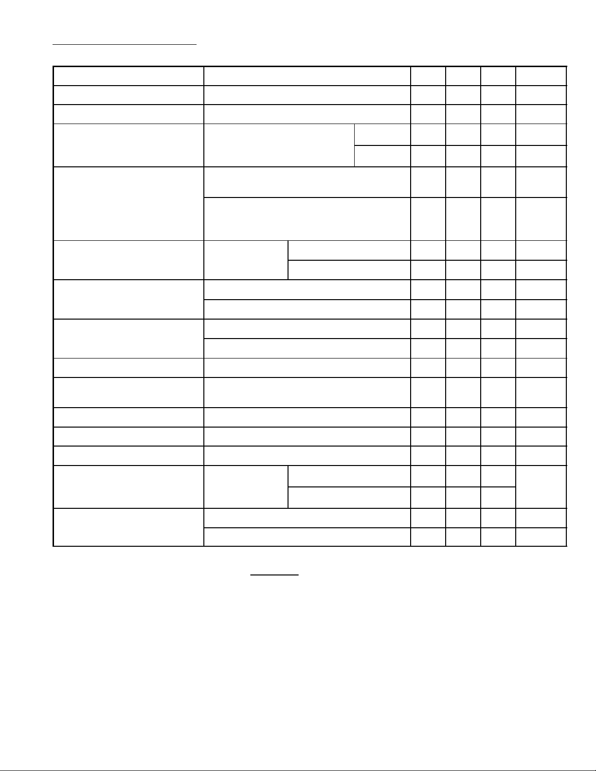
Electrical Characteristics:
(–0°C ≤ TJ ≤ 125°C, VIN = 10V, I
= 0.1µF, unless otherwise specified.)
C
OUT
= 500mA, CIN = 0.33µF,
OUT
Parameter Test Conditions (Note 1, Note 3) Min Typ Max Unit
Input Voltage Range TJ = 25°C 7.5 – 40 V
Output Voltage Range VIN = V
Output Voltage Tolerance
V
OUT
5mA ≤ I
≤ 15W, V
P
D
Line Regulation
TJ = 25°C, V
(V
OUT
TJ = 25°C, V
(V
OUT
(V
OUT
Load Regulation
Control Pin Current
TJ = 25°C,
TJ = 25 C,
= V
V
IN
TJ = 25°C – 1.0 5.0 µA
+5V 5.0 – 30 V
OUT
+3V ≤ VIN ≤ V
≤ 1.0A,
OUT
IN (max)
OUT
= 38V
≤ 10V,
2.5V) ≤ VIN ≤ (V
≥ 10V,
OUT
+3V) ≤ VIN ≤ (V
+3V) ≤ VIN ≤ (V
250mA ≤ I
+5V
OUT
5mA ≤ I
OUT
+15V,
OUT
OUT
OUT
OUT
TJ = 25°C – – 4.0 %(V
– – 5.0 %(V
+20V) – – 1.0
+15V)
+7V)
≤ 750mA – – 1.0 %(V
OUT
–
–
–
–
≤ 1.5A – – 2.0 %(V
%(V
%(V
0.75
0.67
– – 8.0 µA
Quiescent Current
TJ = 25°C – 3.2 5.0 µA
– – 6.0 µA
Ripple Rejection 8V ≤ VIN ≤ 18V, V
Output Noise Voltage TJ = 25°C, 10Hz ≤ f ≤ 100kHz,
= 5V, I
V
OUT
OUT
= 5V, f = 120Hz 62 78 – dB
OUT
– 8 40 µV/V
= 5mA
Dropout Voltage Note 2 – – 2.5 V
OUT
OUT
OUT
OUT
OUT
OUT
OUT
)
)
)
)
)
)
Short Circuit Current TJ = 25°C, VIN = 30V – 0.75 1.2 A
Peak Output Current TJ = 25°C 1.3 2.2 3.3 A
Average Temperature
Coefficient of
Output Voltage
Control Pin Voltage
V
V
OUT
OUT
I
OUT
= 5V,
= 5V,
= 5mA
TJ = –55°C to +25°C – – 0.4
TJ = +25°C to +150°C – – 0.3
TJ = 25°C 4.8 5.0 5.2 V
mV/°C/
V
OUT
(Reference)
4.75 – 5.25 V
Note 1. V
is defined as:
OUT
V
OUT
=
R1 + R2
(5.0)
R2
Note 2. Dropout Voltage is defined as that input–output voltage differential which causes the output
voltage to decrease by 5% of its initial value.
Note 3. All characteristics except noise voltage and ripple rejection ratio are measured using pulse
techniques (t
≤ 10ms, duty cycle ≤ 5%). Output voltage changes due to changes in internal
W
temperature must be taken into account separately.
Page 3

Design Considerations:
The NTE953 a djustable v oltage r egulator h as a n o utput v oltage w hich v aries f rom V
CONTROL
to typically
(R1 + R2)
V
–2V by V
IN
OUT
= V
CONTROL
R2
The nominal reference in the NTE953 is 5.0V. If we allow 1.0mA to flow in the control string to eliminate bias current effects, we can make R2 = 2.2kΩ. The output voltage is then:
V
= (R1 + R2)V, where R1 and R2 are in kΩs.
OUT
Example: If R2 = 5kΩ and R1 = 10kΩ then
V
= 15V nominal
OUT
By proper wiring of the feedback resistors, load regulation of the device can be improved significantly.
The NTE953 voltage regulator contains thermal–overload protection from excessive power, internal
short–circuit protection which limits each circuit’s maximum current, and output transistor safe–area
protection for reducing the output current as the voltage across each pass transistor is increased.
Although the internal power dissipation is limited, the junction temperature must be kept below the
maximum specified temperature in order to meet data sheet specifications. To calculate the maximum junction temperature or heat sink required, the following thermal resistance values should be
used:
Typ
°C/W
Max
°C/W
Typ
°C/W
Max
°C/W
Θ
JC
Θ
7.5 11 75 80
T
P
D(max)
Θ
= ΘCS + Θ
CA
Solving for TJ:T
Where: T
= Junction Temperature
J
= Ambient Temperature
T
A
= Power Dissipation
P
D
= Junction to Ambient Thermal Resistance
Θ
JA
= Junction to Case Thermal Resistance
Θ
JC
= Case to Ambient Thermal Resistance
Θ
CA
= Case to Heat Sink Resistance
Θ
CS
= Heat Sink to Ambient Thermal Resistance
Θ
SA
=TA + PD (ΘJC + ΘCA) or
J
T
A
J(max)
=
ΘJC + Θ
+ PD ΘJA (Without heat sink)
JC
SA
Θ
JA
– T
CA
A
or
T
J(max)
Θ
(Without a heat sink)
JA
Θ
– T
JA
A
Page 4

.375
(9.52)
.310
(7.87)
Indicating
Mark #1 Pin
.395
(10.05)
.360
(9.14)
Tab
1234
.110
(2.79)
.270
(6.85)
.125
(3.17)
Dia
.955
(24.27)
.135 (3.45)
.250
(6.35)
.100 (2.54)
Pin 1. GND
2. V
IN
3. V
OUT
4. Adjust
Tab GND
 Loading...