

Page 1
ISO
2
-CMOS
MT91L60/61
3 Volt Multi-Featured Codec (MFC)
Advance Information
Features
• Single 2.7-3.6 volt supply operation
• MT91L61 version features a delayed framing
pulse in SSI and ST-BUS modes to facilitate
cascaded devices
• Programmable µ-Law/A-Law Codec and Filters
• Programmable ITU-T (G.711)/sign-magnitude
coding
• Programmable transmit, receive and side-tone
gains
• Fully differential interface to handset
transducers - including 300 ohm receiver driver
• Flexible digital interface including ST-BUS/SSI
• Serial microport
• Low power operation
• ITU-T G.714 compliant
• Multiple power down modes
Applications
• Battery operated equipment
• Digital telephone sets
• Cellular radio sets
• Local area communications stations
• Pair Gain Systems
• Line cards
DS5224 ISSUE 3 August 1999
Ordering Information
MT91L61AE 24 Pin Plastic DIP (600 mil)
MT91L60AE 24 Pin Plastic DIP (600 mil)
MT91L61AS 24 Pin SOIC
MT91L60AS 20 Pin SOIC
MT91L61AN 24 Pin SSOP
MT91L60AN 20 Pin SSOP
-40°C to +85°C
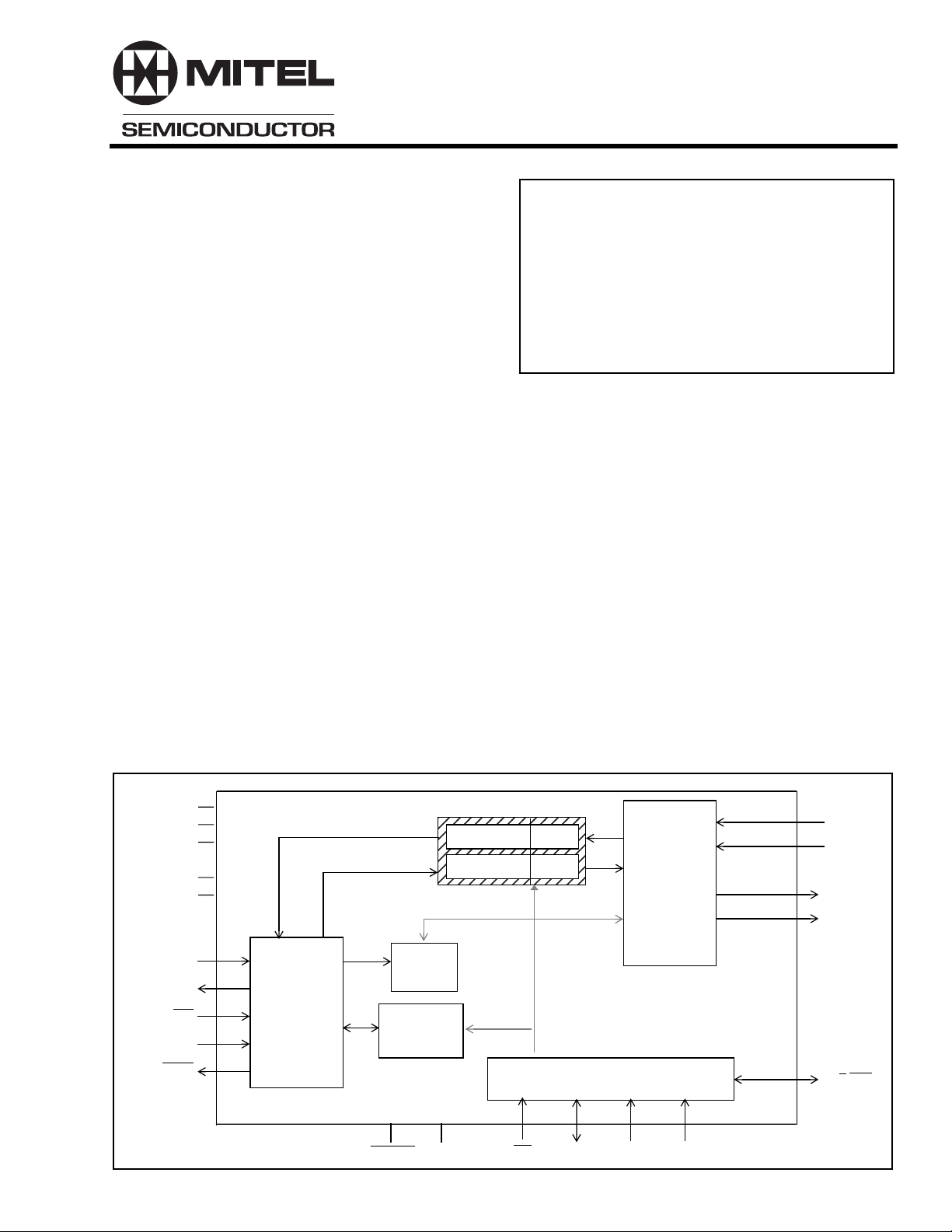
Description
The MT91L60/61 3V Multi-featured Codec
incorporates a built-in Filter/Codec, gain control and
programmable sidetone path as well as on-chip
anti-alias filters, reference voltage and bias source.
The device supports both ITU-T and sign- magnitude
A-Law and µ-Law requirements. The MT91L60/61 is
a true 3V device employing a fully differential
architecture to ensure wide dynamic range.
Complete telephony interfaces are provided for
connection to handset transducers. Internal register
access is provided through a serial microport
compatible with various industry standard
micro-controllers.
The MT91L60/61 is fabricated in Mitel's ISO2-CMOS
technology ensuring low power consumption and
high reliability.
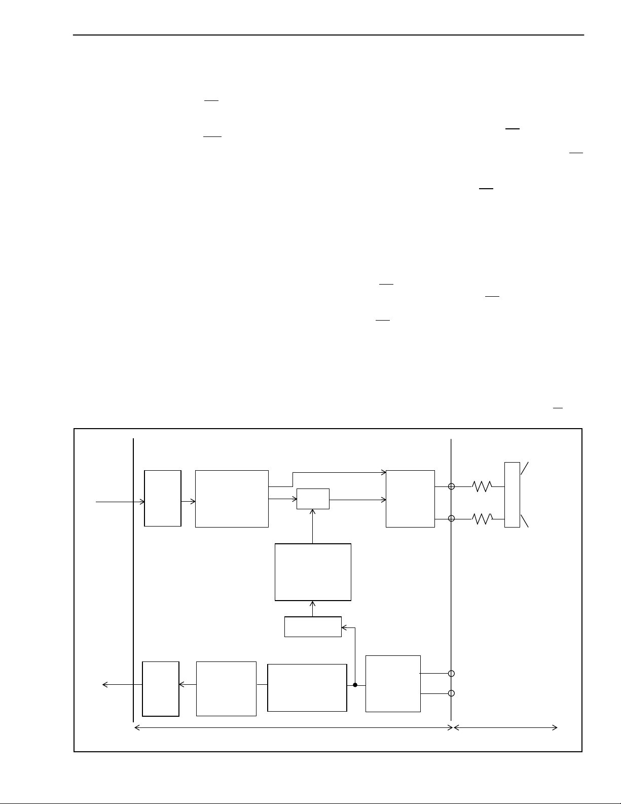
VSSD
VDD
VSSA
VBias
VRef
Din
Dout
STB/F0i
CLOCKin
STBd/FOod
(MT91L61only)
Flexible
Digital
Interface
FILTER/CODEC GAIN
ST-BUS
Channels
PWRST
ENCODER
DECODER
Timing
C & D
IC
7dB
-7dB
Serial Microport
CS DATA1 DATA2 SCLK
Figure 1 - Functional Block Diagram
Transducer
Interface
M M +
HSPKR +
HSPKR -
A/µ/IRQ
1
Page 2
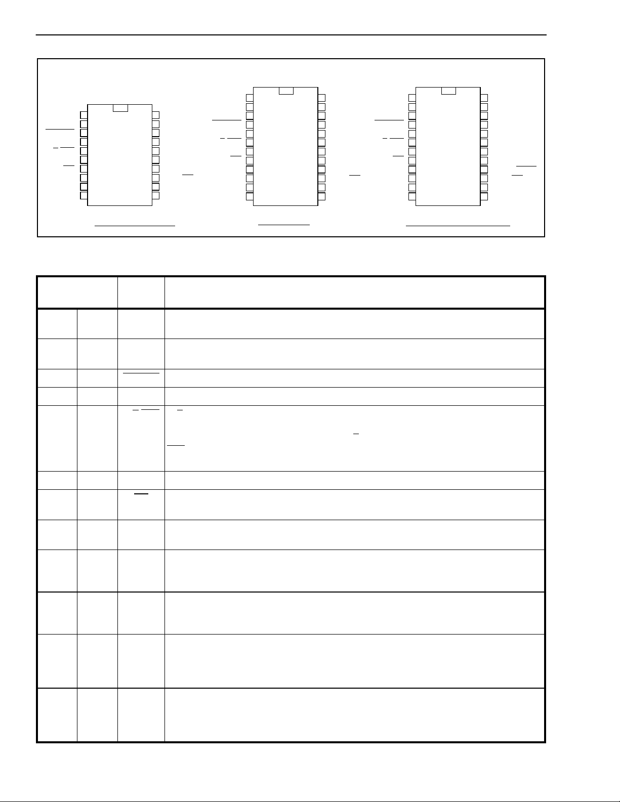
MT91L60/61 Advance Information
MT91L60AE MT91L61AE/AS/AN
VBias
VRef
NC
PWRST
IC
A/µ/IRQ
VSSD
CS
NC
SCLK
DATA1
DATA2
24 PIN PDIP/SOIC/SSOP
NC
IC
CS
NC
1
2
3
4
5
6
7
8
9
10
11
12
24 PIN PDIP
24
23
22
21
20
19
18
17
16
15
14
13
M +
M VSSA
NC
HSPKR +
HSPKR VDD
CLOCKin
NC
F0i
STB/
Din
Dout
10
11
12
1
2
3
4
5
6
7
8
9
24
23
22
21
20
19
18
17
16
15
14
13
M +
M VSSA
NC
HSPKR +
HSPKR VDD
CLOCKin
STBd/
STB/
Din
Dout
VBias
VRef
PWRST
A/
µ/IRQ
VSSD
CS
SCLK
DATA1
DATA2
MT91L60AS/AN
1
2
3
4
IC
5
6
7
8
9
10
20 PIN SOIC/SSOP
20
19
18
17
16
15
14
13
12
11
M +
M VSSA
HSPKR +
HSPKR VDD
CLOCKin
STB/F0i
Din
Dout
VBias
VRef
PWRST
A/µ/IRQ
VSSD
SCLK
DATA1
DATA2
Figure 2 - Pin Connections
Pin Description
Pin #
20 Pin 24 Pin
11V
22V
34PWRST Power-up Reset (Input). CMOS compatible input with Schmitt Trigger (active low).
Name Description
Bias Voltage (Output). (VDD/2) volts is available at this pin for biasing external
Bias
amplifiers. Connect 0.1 µF capacitor to V
Reference Voltage for Codec (Output). Used internally. Nominally [Vdd/2 - 1.1]
Ref
volts. Connect 0.1 µF capacitor to V
SSA
.
SSA
.
FOod
F0i
45ICInternal Connection. Tie externally to V
for normal operation.
SSD
56A/µ/IRQ A/µ - When internal control bit DEn = 0 this CMOS le vel compatib le input pin gov erns
the companding law used by the filter/Codec; µ-Law when tied to V
and A-Law
SSD
when tied to VDD. Logically OR’ed with A/µ register bit.
IRQ - When internal control bit DEn = 1 this pin becomes an open-drain interrupt
output signalling valid access to the D-Channel registers in ST-BUS mode.
67V
Digital Ground. Nominally 0 volts.
SSD
78CS Chip Select (Input). This input signal is used to select the device for microport
data transfers. Active low. CMOS level compatible.
8 10 SCLK Serial Port Synchronous Clock (Input). Data clock for microport. CMOS level
compatible.
9 11 DATA 1 Bidirectional Serial Data. Port for microprocessor serial data transfer. In Motorola/
National mode of operation, this pin becomes the data transmit pin only and data
receive is performed on the DATA 2 pin. Input CMOS level compatible.
10 12 DATA 2 Serial Data Receive. In Motorola/National mode of operation, this pin is used for
data receive. In Intel mode, serial data transmit and receive are performed on the
DATA 1 pin and DATA 2 is disconnected. Input CMOS level compatible.
11 13 D
Data Output. A high impedance three-state digital output for 8 bit wide channel
out
data being sent to the Layer 1 transceiver. Data is shifted out via this pin concurrent
with the rising edge of the bit clock during the timeslot defined by STB, or according
to standard ST-BUS timing.
12 14 D
2
Data Input. A digital input for 8 bit wide channel data received from the Layer 1
in
transceiver. Data is sampled on the falling edge of the bit clock during the timeslot
defined by STB, or according to standard ST-BUS timing. Input level is CMOS
compatible.
Page 3
Advance Information MT91L60/61
Pin Description (continued)
Pin #
20 Pin 24 Pin
Name Description
13 15 STB/F0i Data Strobe/Frame Pulse (Input). For SSI mode this input determines the 8 bit
timeslot used by the device for both transmit and receive data. This active high
signal has a repetition rate of 8 kHz. Standard frame pulse definitions apply in
ST-BUS mode. CMOS level compatible input.
16 STBd/
F0od
(MT91L61
only)
Delayed Frame Pulse Output. In SSI mode, an 8 bit wide strobe is output after the
first strobe goes low. In ST-BUS mode, a frame pulse is output after 4 channel
timeslots.
14 17 CLOCKin Clock (Input). The clock provided to this input pin is used for the internal device
functions. For SSI mode connect the bit clock to this pin when it is 512 kHz or
greater. Connect a 4096 kHz clock to this input when the available bit clock is 128
kHz or 256 kHz. For ST-BUS mode connect C4i to this pin. CMOS level compatible.
15 18 V
Positive Power Supply (Input). Nominally 3 volts.
DD
16 19 HSPKR- Inverting Handset Speaker (Output). Output to the handset speaker (balanced).
17 20 HSPKR+ Non-Inverting Handset Speaker (Output). Output to the handset speaker
(balanced).
18 22 V
Analog Ground (Input). Nominally 0 volts.
SSA
19 23 M- Inverting Microphone (Input). Inverting input to microphone amplifier from the
handset microphone.
20 24 M+ Non-Inverting Microphone (Input). Non-inverting input to microphone amplifier
from the handset microphone.
3,9,
NC No Connect. (24 Packages only). Pin 16 is NC for MT91L60.
16,21
Overview
The 3V Multi-featured Codec (MFC) features
Functional Description
Filter/Codec
complete Analog/Digital and Digital/Analog
conversion of audio signals (Filter/Codec) and an
analog interface to a standard handset transmitter
and receiver (Transducer Interface). The receiver
amplifier is capable of driving a 300 ohm load.
The Filter/Codec block implements conversion of the
analog 0-3.3 kHz speech signals to/from the digital
domain compatible with 64 kb/s PCM B-Channels.
Selection of companding curves and digital code
assignment are programmable. These are ITU-T
Each of the programmable parameters within the
functional blocks is accessed through a serial
microcontroller port compatible with Intel MCS-51®,
Motorola SPI® and National Semiconductor
G.711 A-law or µ-Law, with true-sign/Alternate Digit
Inversion or true-sign/Inverted Magnitude coding,
respectively. Optionally, sign-magnitude coding may
also be selected for proprietary applications.
Microwire® specifications. These parameters
include: gain control, power down, mute, B-Channel
select (ST-BUS mode), C&D channel control/access,
law control, digital interface programming and
loopback. Optionally the device may be used in a
controllerless mode utilizing the power-on default
settings.
The Filter/Codec block also implements transmit and
receive audio path gains in the analog domain. A
programmable gain, voice side-tone path is also
included to provide proportional transmit speech
feedback to the handset receiver. This side tone path
feature is disabled by default. Figure 3 depicts the
nominal half-channel and side-tone gains for the
MT91L60/61.
3
Page 4
MT91L60/61 Preliminary Information
In the event of PWRST, the MT91L60/61 defaults
such that the side-tone path is off, all programmable
gains are set to 0dB and ITU-T µ-Law is selected.
Further, the digital port is set to SSI mode operation
at 2048 kb/s and the FDI and driver sections are
powered up. (See Microport section.)
The internal architecture is fully differential to provide
the best possible noise rejection as well as to allow a
wide dynamic range from a single 3 volt supply
design. This fully differential architecture is
continued into the Transducer Interface section to
provide full chip realization of these capabilities for
the handset functions.
A reference voltage (V
), for the conversion
Ref
requirements of the Codec section, and a bias
voltage (V
sections, are both generated on-chip. V
), for biasing the internal analog
Bias
Bias
is also
brought to an external pin so that it may be used for
biasing external gain setting amplifiers. A 0.1µF
capacitor must be connected from V
ground at all times. Although V
may only be used
Ref
to analog
Bias
internally, a 0.1µF capacitor must be connected from
V
to ground. The analog ground reference point
Ref
for these two capacitors must be physically the same
point. To facilitate this the V
and V
Ref
pins are
Bias
situated on adjacent pins.
The transmit filter is designed to meet ITU-T G.714
specifications. The nominal gain for this filter is 0dB
(gain control = 0dB). Gain control allows the output
signal to be increased up to 7dB. An anti-aliasing
filter is included. This is a second order lowpass
implementation with a corner frequency at 25 kHz.
The receive filter is designed to meet ITU-T G.714
specifications. The nominal gain for this filter is 0dB
(gain control = 0dB). Gain control allows the output
signal to be attenuated up to 7dB. Filter response is
peaked to compensate for the sinx/x attenuation
caused by the 8 kHz sampling rate.
Side-tone is derived from the input of the Tx filter and
is not subject to the gain control of the Tx filter
section. Side-tone is summed into the receive
handset transducer driver path after the Rx filter gain
control section so that Rx gain adjustment will not
affect side-tone levels. The side-tone path may be
enabled/disabled with the gain control bits located in
Gain Control Register 2 (address 01h).
Transmit and receive filter gains are controlled by the
TxFG
-TxFG2 and RxFG0-RxFG2 control bits,
0
respectively. These are located in Gain Control
Register 1 (address 00h). Transmit filter gain is
adjustable from 0dB to +7dB and receive filter gain
from 0dB to -7dB, both in 1dB increments.
Side-tone filter gain is controlled by the STG0-STG
control bits located in Gain Control Register 2
(address 01h). Side-tone gain is adjustable from
-9.96dB to +9.96dB in 3.32dB increments.
Companding law selection for the Filter/Codec is
provided by the A/µ companding control bit while
the coding scheme is controlled by the Smag/ITU-T
control bit. The A/µ control bit is logically OR’ed with
the A/µ pin providing access in both controller and
controllerless modes. Both A/µ and Smag/ITU-T
reside in Control Register 2 (address 04h). Table 1
illustrates these choices.
Code
+ Full Scale 1111 1111 1000 0000 1010 1010
+ Zero 1000 0000 1111 1111 1101 0101
-Zero
(quiet code)
- Full Scale 0111 1111 0000 0000 0010 1010
Sign/
Magnitude
0000 0000 0111 1111 0101 0101
ITU-T (G.711)
µ-Law A-Law
Table 1
Transducer Interfaces
Standard handset transducer interfaces are provided
by the MT91L60/61. These are:
• The handset microphone inputs (transmitter),
pins M+/M-. The nominal transmit path gain may
be adjusted to either 6.0 dB or 15.3 dB. Control of
this gain is provided by the TxINC control bit
(Gain Control register 1, address 00h).
• The handset speaker outputs (receiver), pins
HSPKR+/HSPKR-.This internally compensated
fully differential output driver is capable of driving
the load shown in Figure 3. The nominal receive
path gain may be adjusted to either 0 dB, -6 dB or
-12 dB. Control of this gain is provided by the
RxINC control bit (Gain Control register 1,
address 00h). This gain adjustment is in addition
to the programmable gain provided by the receive
filter.
Microport
The serial microport, compatible with Intel MCS-51
(mode 0), Motorola SPI (CPOL=0,CPHA=0) and
2
Intel® and MCS-51® are registered trademarks of Intel Corporation
Motorola® and SPI® are registered trademarks of Motorola Corporation
National® and Microwire® are trademarks of National Semiconductor Corporation
4
Page 5
Advance Information MT91L60/61
National Semiconductor Microwire specifications
provides access to all MT91L60/61 internal read and
write registers. This microport consists of a transmit/
receive data pin (DATA1), a receive data pin
(DATA2), a chip select pin (CS) and a synchronous
data clock pin (SCLK). For D-channel contention
control, in ST-BUS mode, this interface provides an
open-drain interrupt output (IRQ).
The microport dynamically senses the state of the
serial clock (SCLK) each time chip select becomes
active. The device then automatically adjusts its
internal timing and pin configuration to conform to
Intel or Motorola/National requirements. If SCLK is
high during chip select activation then Intel mode 0
timing is assumed. The DATA1 pin is defined as a
bi-directional (transmit/receive) serial port and
DATA2 is internally disconnected. If SCLK is low
during chip select activation then Motorola/National
timing is assumed. Motorola processor mode
CPOL=0, CPHA=0 must be used. DATA1 is defined
as the data transmit pin while DATA2 becomes the
data receive pin. Although the dual port Motorola
controller configuration usually supports full-duplex
communication, only half-duplex communication is
possible in the MT91L60/61. The micro must discard
non-valid data which it clocks in during a valid write
transfer to the MT91L60/61. During a valid read
transfer from the MT91L60/61 data simultaneously
clocked out by the micro is ignored by the MT91L60/
61.
All data transfers through the microport are two-byte
transfers requiring the transmission of a Command/
Address byte followed by the data byte written or
read from the addressed register. CS must remain
asserted for the duration of this two-byte transfer. As
shown in Figures 5 and 6 the falling edge of CS
indicates to the MT91L60/61 that a microport
transfer is about to begin. The first 8 clock cycles of
SCLK after the falling edge of CS are always used to
receive the Command/Address byte from the
microcontroller. The Command/Address byte
contains information detailing whether the second
byte transfer will be a read or a write operation and
at what address. The next 8 clock cycles are used to
transfer the data byte between the MT91L60/61 and
the microcontroller. At the end of the two-byte
transfer CS is brought high again to terminate the
session. The rising edge of CS will tri-state the
output driver of DATA1 which will remain tri-stated as
long as CS is high.
Intel processors utilize least significant bit first
transmission while Motorola/National processors
employ most significant bit first transmission. The
MT91L60/61 microport automatically
accommodates these two schemes for normal data
bytes. However, to ensure decoding of the R/W and
Serial
D
in
D
out
PCM
PCM
Port
Decoder
Encoder
Filter/Codec and Transducer Interface
Default Bypass
Receive
Filter Gain
0 to -7 dB
(1 dB steps)
Transmit Filter
Gain
Gain
0 to +7 dB
0 to +7 dB
(1 dB steps)
-0.37 dB or 8.93 dB
Internal To Device External To Device
-6 dB
Side-tone
-9.96 to
+9. 96 dB
(3.32 dB steps)
-11 dB
Transmit Gain
-6.0 dB or
0 dB
Receiver
Driver
Default Side-tone off
Transmit
Gain
6.37 dB
HSPKR +
75Ω
HSPKR -
75Ω
M+
M-
Transmitter
Microphone
Handset
Receiver
(150Ω)
Figure 3 - Audio Gain Partitioning
5
Page 6

MT91L60/61 Preliminary Information
address information, the Command/Address byte is
defined differently for Intel operation than it is for
Motorola/National operation. Refer to the relative
timing diagrams of Figures 5 and 6.
Receive data is sampled on the rising edge of SCLK
while transmit data is made available concurrent with
the falling edge of SCLK.
Flexible Digital Interface
A serial link is required to transport data between the
MT91L60/61 and an external digital transmission
device. The MT91L60/61 utilizes the ST-BUS
architecture defined by Mitel Semiconductor but also
supports a strobed data interface found on many
standard Codec devices. This interface is commonly
referred to as Simple Serial Interface (SSI). The
combination of ST-BUS and SSI provides a Flexible
Digital Interface (FDI) capable of supporting all Mitel
basic rate transmission devices as well as many
other 2B+D transceivers.
The required mode of operation is selected via the
CSL2-0 control bits (Control Register 2, address
04h). Pin definitions alter dependent upon the
operational mode selected, as described in the
following subsections as well as in the Pin
Description tables.
logic low coincident with a falling edge of C4i. Refer
to Figure 11 for detailed ST-BUS timing. C4i has a
frequency (4096 kHz) which is twice the data rate.
This clock is used to sample the data at the 3/4
bit-cell position on DSTi and to make data available
on DSTo at the start of the bit-cell. C4iis also used to
clock the MT91L60/61 internal functions (i.e., Filter/
Codec, Digital gain and tone generation) and to
provide the channel timing requirements.
The MT91L60/61 uses only the first four channels of
the 32 channel frame. These channels are always
defined, beginning with Channel 0 after the frame
pulse, as shown in Figure 6 (ST-BUS channel
assignments). The MT91L60/61 provides a delayed
frame pulse (F0od), 4 channels after the input frame
pulse.
The first two (D & C) Channels are enabled for use
by the DEN and CEN bits respectively, (Control
Register 2, address 04h). ISDN basic rate service
(2B+D) defines a 16 kb/s signalling (D) Channel. The
MT91L60/61 supports transparent access to this
signalling channel. ST-BUS basic rate transmission
devices, which may not employ a microport, provide
access to their internal control/status registers
through the ST-BUS Control (C) Channel. The
MT91L60/61 supports microport access to this
C-Channel.
Quiet Code
The FDI can be made to send quiet code to the
decoder and receive filter path by setting the RxMute
bit high. Likewise, the FDI will send quiet code in the
transmit path when the TxMute bit is high. Both of
these control bits reside in Control Register 1 at
address 03h. When either of these bits are low their
respective paths function normally. The -Zero entr y
of Table 1 is used for the quiet code definition.
ST-BUS Mode
The ST-BUS consists of output (DSTo) and input
(DSTi) serial data streams, in FDI these are named
Dout and Din respectively, a synchronous clock input
signal CLOCKin (
(F0i). These signals are direct connections to the
corresponding pins of Mitel basic rate devices. The
CSL2, CSL1 and CSL0 bits are set to 1 for ST-BUS
operation.
The data streams operate at 2048 kb/s and are Time
Division Multiplexed into 32 identical channels of 64
kb/s bandwidth. A frame pulse (a 244 nSec low going
pulse) is used to separate the continuous serial data
streams into the 32 channel TDM frames. Each
frame has a 125 µSecond period translating into an 8
kHz frame rate. A valid frame begins when
C4i), and a framing pulse input
F0i is
DEN - D-Channel
In ST-BUS mode access to the D-Channel (transmit
and receive) data is provided through an 8-bit read/
write register (address 06h). D-Channel data is
accumulated in, or transmitted from this register at
the rate of 2 bits/frame for 16 kb/s operation (1 bit/
frame for 8 kb/s operation). Since the ST-BUS is
asynchronous, with respect to the microport, valid
access to this register is controlled through the use
of an interrupt (IRQ) output. D-Channel access is
enabled via the (DEn) bit.
DEN:
When 1, ST-BUS D-channel data (1 or 2 bits/frame
depending on the state of the D8 bit) is shifted into/
out of the D-channel (READ/WRITE) register.
When 0, the receive D-channel data (READ) is still
shifted into the proper register while the DSTo
D-channel timeslot and IRQ outputs are tri-stated
(default).
D8:
When 1, D-Channel data is shifted at the rate of 1 bit/
frame (8 kb/s).
6
Page 7
Advance Information MT91L60/61
When 0, D-Channel data is shifted at the rate of 2
bits/frame (16 kb/s default).
frame. By arbitrarily assigning ST-BUS frame n as
the reference frame, during which the
microprocessor D-Channel read and write operations
16 kb/s D-Channel operation is the default mode
are performed, then:
which allows the microprocessor access to a full byte
of D-Channel information every fourth ST-BUS
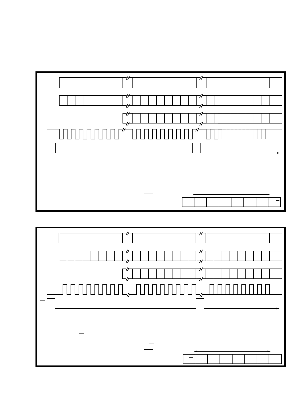
COMMAND/ADDRESS DATA INPUT/OUTPUT COMMAND/ADDRESS:
DATA 1
RECEIVE
DATA 1
TRANSMIT
SCLK
CS
➀ Delays due to internal processor timing which are transparent.
② The MT91L60/L61:latches received data on the rising edge of SCLK.
➂ The falling edge of
subsequent byte is always data until terminated via
➃ A new COMMAND/ADDRESS byte may be loaded only by CS cycling high then low again.
➄ The COMMAND/ADDRESS byte contains:
D0D1D2D3D4D5D6D
②
➂
-outputs transmit data on the falling edge of SCLK.
CS indicates that a COMMAND/ADDRESS byte will be transmitted from the microprocessor. The
➄
➀
D
7
0D1D2D3D4D5D6D7
D0D1D2D3D4D5D6D
CS returning high.
1 bit - Read/
3 bits - Addressing Data
4 bits - Unused
Write
7
D
7
XX A2A1A
➀
➃
➂
➃
D0D1D2D3D4D5D6D
D0D1D2D3D4D5D6D
XX
7
7
D
0
R/W
0
Figure 4 - Serial Port Relative Timing for Intel Mode 0
COMMAND/ADDRESS DATA INPUT/OUTPUT COMMAND/ADDRESS:
DATA 2
RECEIVE
DATA 1
TRANSMIT
SCLK
CS
➀ Delays due to internal processor timing which are transparent .
② The MT91L60/L61: latches received data on the rising edge of SCLK.
➂ The falling edge of
subsequent byte is always data until terminated via
➃ A new COMMAND/ADDRESS byte may be loaded only by CS cycling high then low again.
➄ The COMMAND/ADDRESS byte contains:
D7D6D5D4D3D2D1D
②
➂
-outputs transmit data on the falling edge of SCLK.
CS indicates that a COMMAND/ADDRESS byte will be transmitted from the microprocessor. The
➄
➀
D7D6D5D4D3D2D1D
0
D7D6D5D4D3D2D1D
CS returning high.
1 bit - Read/
3 bits - Addressing Data
4 bits - Unused
Write
0
0
➃
D
7
R/WX A1A
➀
➃
D7D6D5D4D3D2D1D
D7D6D5D4D3D2D1D
➂
XX
A
2
0
0
D
0
X
0
Figure 5 - Serial Port Relative Timing for Motorola Mode 00/National Microwire
7
Page 8
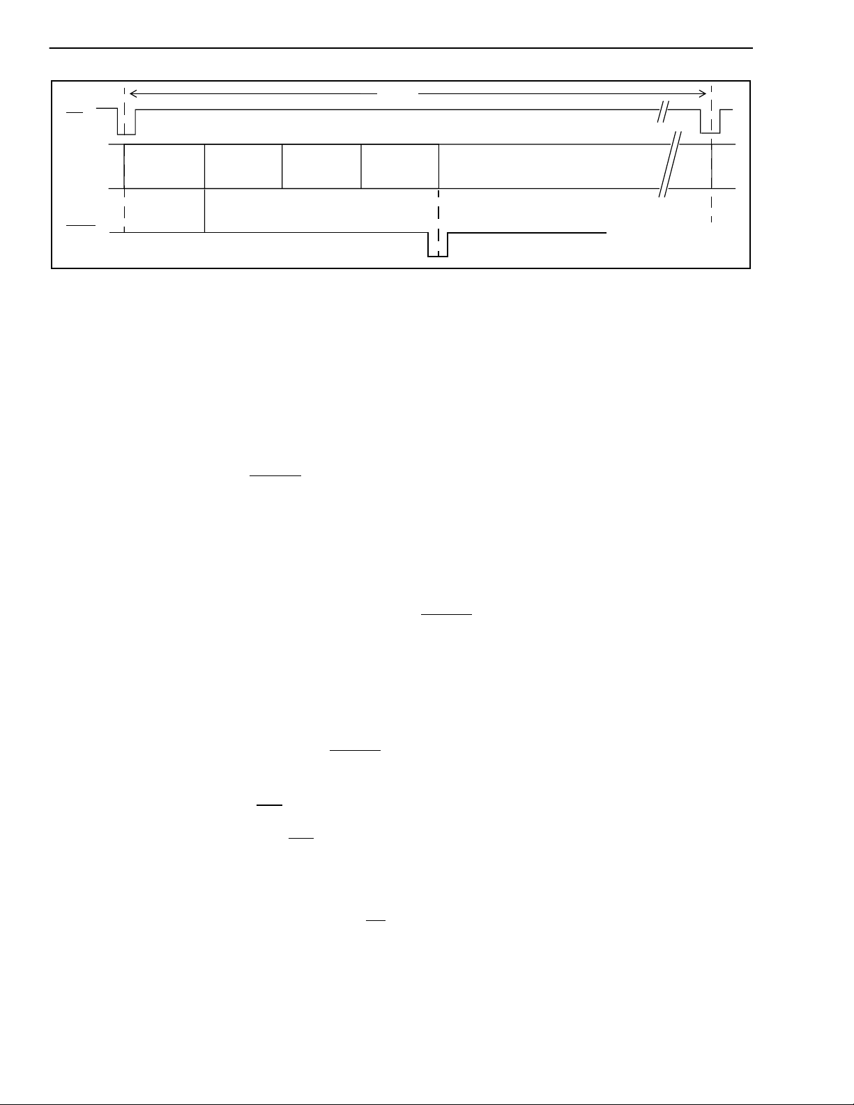
MT91L60/61 Advance Information
125 µs
F0i
DSTi,
DSTo
FOod
CHANNEL 0
D-channel
LSB first
for D-
Channel
CHANNEL 1
C-channel
CHANNEL 2
B1-channel
MSB first for C, B1- & B2-
Channels
CHANNEL 3
B2-channel
Figure 6 - ST-BUS Channel Assignment
(a) A microport read of address 04 hex will result in a
byte of data being extracted which is composed of
four di-bits (designated by roman numerals I,II,III,IV).
These di-bits are composed of the two D-Channel
bits received during each of frames n, n-1, n-2 and
n-3. Referring to Fig. 7a: di-bit I is mapped from
frame n-3, di-bit II is mapped from frame n-2, di-bit III
is mapped from frame n-1 and di-bit IV is mapped
from frame n.
The D-Channel read register is not preset to any
particular value on power-up (PWRST) or software
reset (RST).
(b) A microport write to Address 04 hex will result in
a byte of data being loaded which is composed of
four di-bits (designated by roman numerals I, II, III,
IV). These di-bits are destined for the two D-Channel
bits transmitted during each of frames n+1, n+2, n+3,
n+4. Referring to Fig. 7a: di-bit I is mapped to frame
n+1, di-bit II is mapped to frame n+2, di bit III is
mapped to frame n+3 and di bit IV is mapped to
frame n+4.
CHANNELS 4-31
Not Used
8 kb/s operation expands the interrupt to every eight
frames and processes data one-bit-per-frame.
D-Channel register data is mapped according to
Figure 7c.
CEn - C-Channel
Channel 1 conveys the control/status information for
the Layer 1 transceiver. C-Channel data is
transferred MSB first on the ST-BUS by the
MT91L60/61. The full 64 kb/s bandwidth is available
and is assigned according to which transceiver is
being used. Consult the data sheet for the selected
transceiver for its C-Channel bit definitions and order
of bit transfer.
When CEN is high, data written to the C-Channel
register (address 05h) is transmitted, most
significant bit first, on DSTo. On power-up reset
(PWRST) or software reset (Rst, address 03h) all
C-Channel bits default to logic high. Receive
C-Channel data (DSTi) is always routed to the read
register regardless of this control bit's logic state.
If no new data is written to address 04 hex , the
current D-channel register contents will be
continuously re-transmitted. The D-Channel write
register is preset to all ones on power-up (PWRST)
or software reset (RST).
An interrupt output is provided (IRQ) to synchronize
microprocessor access to the D-Channel register
during valid ST-BUS periods only. IRQ will occur
every fourth (eighth in 8 kb/s mode) ST-BUS frame
at the beginning of the third (second in 8 kb/s mode)
ST-BUS bit cell period. The interrupt will be removed
following a microprocessor Read or Write of Address
04 hex or upon encountering the following fr amesF0i
input, whichever occurs first. To ensure D-Channel
data integrity, microport read/write access to
Address 04 hex must occur before the following
frame pulse. See Figure 7b for timing.
8
When low, data transmission is halted and this
timeslot is tri-stated on DSTo.
B1-Channel and B2-Channel
Channels 2 and 3 are the B1 and B2 channels,
respectively. B-channel PCM associated with the
Filter/Codec and transducer audio paths is selected
on an independent basis for the transmit and receive
paths. TxBSel and RxBSel (Control Register 1,
address 03h) are used for this purpose.
If no valid transmit path has been selected then the
timeslot output on DSTo is tri-stated (see PDFDI and
PDDR control bits, Control Register 1 address 03h).
Page 9
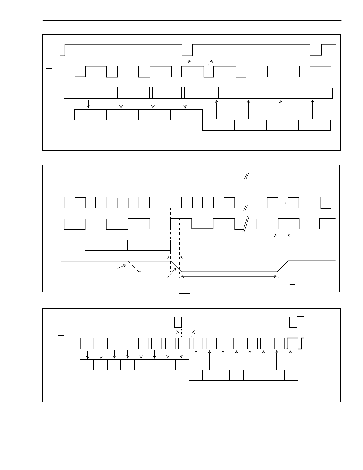
Advance Information MT91L60/61
IRQ
Microport Read/Write Access
FP
DSTo/
DSTi
n-3 n-2 n-1 n n+1 n+2 n+3 n+4*
Di-bit Group
Receive
D-Channel
D0
I
D2
II
D1
No preset value
D3
D4
III
D5
* note that frame n+4 is equivalent to frame n of the next cycle.
Figure 7a - D-Channel 16 kb/s Operation
FP
C4i
C2
DSTo/
DSTi
IRQ
D0
8 kb/s operation
D1
16 kb/s operation
IV
D6
D7
Di-bit Group
Transmit
D-Channel
tif=500 nsec max
Microport Read/Write Access
D0
I
D1
D2
II
D3
D4
III
D5
D6
IV
D7
Power-up reset to 1111 1111
tir=500 nsec max
R
= 10 k
pullup
Reset coincident with
Read/Write of Address 04 Hex
or next
FP, whichever occurs first
IRQ
FP
Di-bit Group
Receive
D-Channel
Figure 7b - IRQ Timing Diagram
n-7 n-6 n-5 n-4 n-3 n-2 n-1 n n+1
IID1IIID2IV
I
D0
No preset value
D3
V
D4
VID5VIID6VIII
D7
Di-bit Group
Transmit
D-Channel
Figure 7c - D-Channel 8 kb/s Operation
Microport Read/Write Access
I
D0
n+2
IID1IIID2IV
n+3
n+4
D3
Power-up reset to 1111 1111
n+5
VID5VIID6VIII
V
D4
n+6
n+7
n+8
D-Channel
D7
9
Page 10

MT91L60/61 Preliminary Information
SSI Mode
The SSI BUS consists of input and output serial data
streams named Din and Dout respectively, a Clock
input signal (CLOCKin), and a framing strobe input
(STB). The frame strobe must be synchronous with,
and eight cycles of, the bit clock. A 4.096 MHz
master clock is also required for SSI operation if the
bit clock is less than 512 kHz. The timing
requirements for SSI are shown in Figures 12 & 13.
In SSI mode the MT91L60/61 supports only
B-Channel operation. The internal C and D Channel
registers used in ST-BUS mode are not functional for
SSI operation. The control bits TxBSel and RxBSel,
as described in the ST-BUS section, are ignored
since the B-Channel timeslot is defined by the input
STB strobe. Hence, in SSI mode transmit and
receive B-Channel data are always in the channel
defined by the STB input.
The data strobe input STB determines the 8-bit
timeslot used by the device for both transmit and
receive data. This is an active high signal with an 8
kHz repetition rate. The MT91L61 provides a
delayed strobe pulse which occurs after the initial
strobe goes low and is held high for the duration of 8
pcm bits.
SSI operation is separated into two categories based
upon the data rate of the available bit clock. If the bit
clock is 512 kHz or greater then it is used directly by
the internal MT91L60/61 functions allowing
synchronous operation. If the available bit clock is
128 kHz or 256 kHz, then a 4096 kHz master clock is
required to derive clocks for the internal MT91L60/61
functions.
Applications where Bit Clock (BCL) is below 512 kHz
are designated as asynchronous. The MT91L60/61
will re-align its internal clocks to allow operation
when the external master and bit clocks are
asynchronous. Control bits CSL2, CSL1 and CSL0 in
Control Register 2 (address 04h) are used to
program the bit rates.
For asynchronous operation Dout and Din are as
defined for synchronous operation except that the
allowed output jitter on Dout is larger. This is due to
the resynchronization circuitry activity and will not
affect operation since the bit cell period at 128 kb/s
and 256 kb/s is relatively large. There is a one frame
delay through the FDI circuit for asynchronous
operation. Refer to the specifications of Figures 12
& 13 for both synchronous and asynchronous SSI
timing.
PWRST/Software Reset (Rst)
While the MT91L60/61 is held in PWRST no d evice
control or functionality is possible. While in software
reset (Rst=1, address 03h) only the microport is
functional. Software reset can only be removed by
writing the Rst bit low or by performing a hardware
PWRST. While the Rst bit is high, the other bits in
Control Register 1 are held low and cannot be
reprogrammed. Therefore to modify Control Register
1 the Rst bit must first be written low, followed by a
2nd write operation which writes the desired data.
This avoids a race condition between clearing the
reset bit and the writing of the other bits in Control
Register 1.
After a Power-up reset (PWRST) or software reset
(Rst) all control bits assume their "Power Reset
Value" default states; µ-Law coding, 0 dB Rx and
6dB Tx gains and the device powered up in SSI
mode 2048 kb/s operation with Dout tri-stated while
there is no strobe active on STB. If a valid strobe is
supplied to STB, then Dout will be active, during the
defined channel.
To attain complete power-down from a normal
operating condition, write PDFDI = 1 and PDDR = 1
(Control Register 1, address 03h) or set the PWRST
pin low.
For synchronous operation data is sampled, from
Din, on the falling edge of BCL during the time slot
defined by the STB input. Data is made available, on
Dout, on the rising edge of BCL during the time slot
defined by the STB input. Dout is tri-stated at all
times when STB is not true. If STB is valid and
PDDR is set, then quiet code will be transmitted on
Dout during the valid strobe period. There is no
frame delay through the FDI circuit for synchronous
operation.
10
Page 11

Advance Information MT91L60/61
Applications
Figure 8 shows an application in a wireless phone
set. Figure 9 shows an MT9161B’s delayed frame
pulse driving a second MT9161B. This configuration
would be used where multiple CODEC’s were using
a data bus (an example being Mitel’s ST-BUS).
00 RxINC RxFG
RxFG
2
RxFG
1
TxINC TxFG
0
TxFG
2
TxFG
1
0
Gain Control
Register 1
01-----STG2STG
STG
1
0
Gain Control
Register 2
02-------DrGain Path Control
03 PDFDI PDDR RST - TxMute RxMute TxBsel RxBsel Control Register 1
04 CEN DEN D8 A/µ Smag/
CSL
CSL
2
CSL0Control Register 2
1
ITU-T
05 C
7
C
6
C
5
C
4
C
3
C
2
C
1
C
0
C-Channel
Register
06 D
7
D
6
D
5
D
4
D
3
D
2
D
1
D
0
D-Channel
Register
07----PCM/
loopen - - Loop Back
ANALOG
Table 2: 3V Multi-featured Codec Register Map
Note: Bits marked "-" are reserved bits and should be written with logic "0"
11
Page 12

MT91L60/61 Advance Information
330Ω
10 µF
511Ω
+3V
0.1 µF
100K
+
+
R
M+
10 µF
330Ω
+
+3V
1K
0.1 µF
VBias
T
+
-
R
M+
Electret
Microphone
3V
INTEL
MCS-51
or
MOTOROLA
SPI
Micro-
Controller
+
+3V
511Ω
0.1 µF
0.1 µF
0.1 µF
100K
VBias
0.1 µF
100K
Differential Amplifier
VBias
A/µ/IRQ
CS
SCLK
DATA1
DATA2
DATA2 Motorola
Mode only
Av = 1 + 2R
T
+
+3V
+
Single-ended Amplifier
75Ω
75Ω
20
19
18
17
16
15
14
13
12
11
Electret
Microphone
T
R
M-
Typical External Gain
()
1
2
3
4
MT91L60
5
6
7
8
9
10
AV= 5-10
M+
M-
VBias
M-
150Ω
Wireless
Phone
Baseband
Processer
Figure 8 - Wireless Phone Set
Din
Dout
Frame Pulse
Clock
12
Page 13

Advance Information MT91L60/61
+3V
3V
INTEL
MCS-51
or
MOTOROLA
SPI
Micro-
Controller
100K
0.1 µF
0.1 µF
0.1 µF
0.1 µF
A/µ/IRQ
CS
VBias
SCLK
DATA1
DATA2
DATA2 Motorola
Mode only
VBias
Typical External Gain
()
1
2
3
4
5
6
MT91L61
7
8
9
10
11
12
AV= 5-10
24
23
22
21
20
19
18
17
16
15
14
13
75Ω
+3V
Timing
from
PC Bus
75Ω
Din
Dout
Frame Pulse
Clock
M+
M-
150Ω
MM+
0.1 µF
+3V
A/µ/IRQ
CS
SCLK
DATA1
DATA2
DATA2 Motorola
Mode only
1
2
3
4
5
6
7
8
9
10
11
12
MT91L61
24
23
22
21
20
19
18
17
16
15
14
13
+3V
75Ω
75Ω
Figure 9 - Delayed Frame Pulse of First MT91L61 Signalling Second MT91L61
150Ω
13
Page 14

MT91L60/61 Advance Information
Register Summary
Gain Control Register 1 ADDRESS = 00h WRITE/READ VERIFY
Power Reset Value
RxINC
RxFG2RxFG1RxFG
0
TxINC
TxFG2TxFG1TxFG
76543210
0
1000 0000
Receive Gain
Setting (dB)
(default) 0
-1
-2
-3
-4
-5
-6
-7
RxFGn = Receive Filter Gain bit n
RxINC: When high, the receive path nominal gain is set to 0 dB. When low, this gain is -6.0 dB.
TxINC: When high, the transmit path nominal gain is set to 15.3 dB. When low, this gain is 6.0 dB.
RxFG
0
0
0
0
1
1
1
1
RxFG
2
0
0
1
1
0
0
1
1
RxFG
1
0
0
1
0
1
0
1
0
1
Transmit Gain
Setting (dB)
(default) 0
1
2
3
4
5
6
7
TxFGn = Transmit Filter Gain bit n
TxFG
TxFG
2
0
0
0
0
1
1
1
1
0
0
1
1
0
0
1
1
TxFG
1
0
0
1
0
1
0
1
0
1
Gain Control Register 2 ADDRESS = 01h WRITE/READ VERIFY
Power Reset Value
---- STG2STG1STG
-
0
XXXX X000
76543210
14
Side-tone Gain
Setting (dB)
(default) OFF
-9.96
-6.64
-3.32
0
3.32
6.64
9.96
STGn = Side-tone Gain bit n
STG
0
0
0
0
1
1
1
1
2
STG
0
0
1
1
0
0
1
1
STG
1
0
0
1
0
1
0
1
0
1
Note: Bits marked "-" are reserved bits and should be written with logic "0"
Page 15

Advance Information MT91L60/61
Path Control
ADDRESS = 02h WRITE/READ VERIFY
Power Reset Value
---
-
-
--
DrGain
XX00 0000
76543210
DrGain When high, the receive path is summed with the side tone path and is attenuated by 6dB.
When low, the receive path conatins no side tone (default).
Control Register 1
PDFDI PDDR TxBsel RxBselRst
_
TxMute RxMute
ADDRESS = 03h WRITE/READ VERIFY
Power Reset Value
0000 0000
76543210
PDFDI When high, the FDI PLA and the Filter/Codec are powered down (default). When low, the FDI is active.
PDDR When high, the ear driver and Filter/Codec are powered down (default). In addition, in ST-BUS mode, the selected
Rst When high, a software reset occurs performing the same function as the hardware reset (PWRST) except that the Rst
TxMute When high the transmit PCM stream is interrupted and replaced with quiet code; thus forcing the output code into a
RxMute When high the received PCM stream is interrupted and replaced with quiet code; thus forcing the receive path into a
TxBsel When high, the transmit B2 channel is functional in ST-BUS mode. When low, the transmit B1 channel is functional in
RxBsel When high, the receive B2 channel is functional in ST-BUS mode. When low, the receive B1 channel is functional in
output channel is tri-stated. In SSI mode the PCM output code will be -zero code during the valid strobe period. The
output will be tri-stated outside of the valid strobe and for the whole frame if no strobe is supplied. When low, the driver
and Filter/Codec are active if PDFDI is low.
bit remains high and device remains powered up. A software reset can be removed only by writing this bit low or by
means of a hardware reset (PWRST). This bit is useful for quickly programming the Registers to the default Power
Reset Values. When this bit is low, the reset condition is removed allowing the registers to be modified
mute state (only the output code is muted, the transmit microphone and transmit Filter/Codec are still functional). When
low the full transmit path functions normally (default).
mute state. When low the full receive path functions normally (default).
ST-BUS mode. Not used in SSI mode.
Note: Bits marked "-" are reserved bits and should be written with logic "0"
15
Page 16

MT91L60/61 Advance Information
Control Register 2 ADDRESS = 04h WRITE/READ VERIFY
Power Reset Value
0000 0010
CEn DEn
D8
A/µ
Smag/
ITU-T
CSL
CSL1CSL
2
0
76543210
CEn When high, data written into the C-Channel register (address 05h) is transmitted during channel 1 on DSTo. When
DEn When high, data written into the D-Channel Register (address 06h) is transmitted (2 bits/frame) during channel 0
D8 When high, D-channel operates at 8kb/s. When low, D-channel operates at 16kb/s (default).
A/µ When high, A-Law encoding/decoding is selected for the MT91L60/61. When low, µ-Law encoding/decoding is
Smag/ITU-T When high, sign-magnitude code assignment is selected for the Codec input/output. When low, ITU-T code
CSL
low, the channel 1 timeslot is tri-stated on DSTo. Channel 1 data received on DSTi is read via the C-Channel
register (address 05h) regardless of the state of CEn. This control bit has significance only for ST-BUS operation
and is ignored for SSI operation.
on DSTo. The remaining six bits of the D-Channel carry no information. When low, the channel 0 timeslot is
completely tri-stated on DSTo. Channel 0 data received on DSTi is read via the D-Channel register regardless of
the state of DEN. This control bit has significance only for ST-BUS mode and is ignored for SSI operation.
selected.
assignment is selected for the Codec input/output; true sign, inverted magnitude (µ-Law) or true sign, alternate
digit inversion (A-Law).
CSL
2
1 1 1 N/A 4096 ST-BUS
1 0 0 128 4096 SSI
1 0 1 256 4096 SSI
0 0 0 512 512 SSI
0 0 1 1536 1536 SSI
0 1 0 2048 2048 SSI (default)
0 1 1 4096 4096 SSI
CSL
1
Bit Clock rate (kHz) CLOCKin (kHz) Mode
0
16
Note: Bits marked "-" are reserved bits and should be written with logic "0"
Page 17

Advance Information MT91L60/61
C-Channel Register ADDRESS = 05h WRITE/READ
Power Reset Value
C7 C6 C5 C4 C2 C1 C0C3
76543210
Micro-port access to the ST-BUS C-Channel information read and write
1111 1111- write
XXXX XXXX - read
D-Channel Register
D7 D6 D5 D4 D2 D1 D0D3
ADDRESS = 06h WRITE/READ
Power Reset Value
1111 1111- write
XXXX XXXX - read
76543210
D7-D0 Data written to this register will be transmitted every frame, in channel 0, if the DEn control bit is set (address 04h).
Loopback Register
Received D-Channel data is valid, regardless of the state of DEn. These bits are valid for ST-BUS mode only and are
accessible only when IRQ indicates valid access.
ADDRESS = 07h WRITE/READ VERIFY
--
--
-
PCM/
ANALOG
loopen
-
Power Reset Value
XXXX 0000
76543210
PCM/ANALOG This control bit functions only when loopen is set high. It is ignored when loopen is low.
For loopback operation when this bit is high, the device is configured for digital-to-digital loopback operation. Data on
Din is looped back to Dout without conversion to the analog domain. However, the receive D/A path (from Din to
HSPKR ±) still functions. When low, the device is configured for analog-to-analog operation. An analog input signal at
M± is looped back to the SPKR± outputs through the A/D and D/A circuits as well as through the normal transmit A/D
path (from M± to Dout).
loopen When high, loopback operation is enabled and the loopback type is governed by the state of the PCM/ANALOG bit.
When low, loopbacks are disabled, the device operates normally and the PCM/ANALOG bit is ignored.
Din
Dout
Dout
Analog Loopback Digital Loopback
PCM/
ANALOG = 0 loopen = 1
HSPKR +/-
M +/-
Figure 10 - Loopback Signal Flow
Note: Bits marked "-" are reserved bits and should be written with logic "0"
ANALOG = 1 loopen = 1
PCM/
HSPKR +/-
17
Page 18

MT91L60/61 Advance Information
Absolute Maximum Ratings
†
Parameter Symbol Min Max Units
1 Supply Voltage VDD - V
2 Voltage on any I/O pin VI/V
3 Current on any I/O pin (transducers excluded) II/I
4 Storage Temperature T
5 Power Dissipation (package) P
†
Exceeding these values may cause permanent damage. Functional operation under these conditions is not implied.
Recommended Operating Conditions - Voltages are with respect to V
SS
O
O
S
D
SS
- 0.3 5 V
VSS - 0.3 VDD + 0.3 V
- 65 + 150 °C
unless otherwise stated
Characteristics Sym Min Typ Max Units Test Conditions
1 Supply Voltage V
2 CMOS Input Voltage (high) V
3 CMOS Input Voltage (low) V
4 Operating Temperature T
DD
IHC
ILC
A
2.7 3 3.6 V
0.9*V
V
SS
DD
V
DD
0.1*V
DD
- 40 + 85 °C
V
V
± 20 mA
750 mW
Power Characteristics
Characteristics Sym Min Typ Max Units Test Conditions
1 Static Supply Current (clock
disabled, all functions off, PDFDI/
PDDR=1, PWRST=0)
2 Dynamic Supply Current:
Total all functions enabled
Note 1: Power delivered to the load is in addition to the bias current requirements.
I
DDC1
I
DDFT
220µA Outputs unloaded, Input
6 10 mA See Note 1.
signals static, not loaded
18
Page 19

Advance Information MT91L60/61
DC Electrical Characteristics
Characteristics Sym Min Typ
1 Input HIGH Voltage CMOS inputs V
2 Input LOW Voltage CMOS inputs V
3 VBias Voltage Output V
4 VRef Voltage Output V
5 Input Leakage Current I
6 Positive Going Threshold
†
- Voltages are with respect to ground (VSS) unless otherwise stated.
V
IHC
ILC
Bias
Ref
IZ
T+
‡
0.7*Vdd
VDD/2 V Max. Load = 20kΩ
VDD/2-1.1 V No Load
0.1 10 µAVIN=VDD to V
2.2
Max Units Test Conditions
V
0.3*Vdd V
V
Voltage (PWRST only)
Negative Going Threshold
V
T-
0.7
V
Voltage (PWRST only)
Hysteresis
7 Output HIGH Current I
8 Output LOW Current I
9 Output Leakage Current I
10 Output Capacitance C
OH
OL
OZ
o
11 Input Capacitance C
† DC Electrical Characteristics are over recommended temperature range & recommended power supply voltages.
‡ Typical figures are at 25 °C and are for design aid only: not guaranteed and not subject to production testing.
* Note 1 - Magnitude measurement, ignore signs.
1.0 mA VOH = 0.9*V
2.5 mA VOL = 0.1*V
i
0.65
V
0.01 10 µAV
15 pF
10 pF
Vdd = 3V
See Note 1
See Note 1
= VDD and V
OUT
SS
DD
DD
SS
Clockin Tolerance Characteristics† (ST-BUS Mode)
Characteristics Min Typ
1 C4i Frequency 4095.6 4096 4096.4 kHz (i.e., 100 ppm)
† AC Electrical Characteristics are over recommended temperature range & recommended power supply voltages.
‡ Typical figures are at 25 °C and are for design aid only: not guaranteed and not subject to production testing.
‡
Max Units Test Conditions
19
Page 20

MT91L60/61 Advance Information
AC Characteristics† for A/D (Transmit) Path - 0dBm0 = A
- 3.14dB =1.067V
1 Analog input equivalent to
overload decision
2 Absolute half-channel gain
M ± to Dout G
Tolerance at all other transmit
filter settings
(1 to 7dB)
3 Gain tracking vs. input level
ITU-T G.714 Method 2
4 Signal to total Distortion vs. input
level.
ITU-T G.714 Method 2
5 Transmit Idle Channel Noise N
6 Gain relative to gain at 1020Hz
<50Hz
60Hz
200Hz
300 - 3000 Hz
3000-3300 Hz
3300 Hz
3400 Hz
4000 Hz
4600 Hz
>4600 Hz
for A-Law, at the Codec. (V
rms
= 0.4V and V
Ref
=1.5 volts.)
Bias
Characteristics Sym Min Typ
A
A
G
Li3.17
Li3.14
AX1
AX2
5.4
14.7
4.246
4.4
6.0
15.3
-0.2 ±0.1 +0.2 dB
G
TX
-0.3
-0.6
-1.6
D
QX
35
29
24
CX
N
PX
G
RX
13
-70.516-69
-45
-0.25
-0.9
-0.9
-1.2
-0.2
-0.6
-23
-41
‡
- 3.17dB = 1.027V
Lo3.17
for µ-Law and 0dBm0 = A
rms
Max Units Test Conditions
Vp-p
Vp-p
µ-Law
A-Law
Both at Codec
Transmit filter gain=0dB
setting.
6.6
15.9
dB
dB
TxINC = 0*
TxINC = 1*
@1020 Hz
0.3
0.6
1.6
-25
-30
0.0
0.25
0.25
0.25
0.25
-12.5
-25
-25
dB
dB
dB
dB
dB
dB
dBrnC0
dBm0p
dB
dB
dB
dB
dB
dB
dB
dB
dB
dB
3 to -40 dBm0
-40 to -50 dBm0
-50 to -55 dBm0
0 to -30 dBm0
-40 dBm0
-45 dBm0
µ-Law
A-Law
Lo3.14
7 Absolute Delay D
AX
360 µs at frequency of minimum
delay
8 Group Delay relative to D
AX
9 Power Supply Rejection
f=1020 Hz PSSR 30 50 dB
† AC Electrical Characteristics are over recommended temperature range & recommended power supply voltages.
‡ Typical figures are at 25 °C and are for design aid only: not guaranteed and not subject to production testing.
* Note: TxINC, refer to Control Register 1, address 00h.
20
D
DX
750
380
130
750
µs
µs
µs
µs
500-600 Hz
600 - 1000 Hz
1000 - 2600 Hz
2600 - 2800 Hz
±100mV peak signal on
V
DD
µ-law
Page 21

Advance Information MT91L60/61
AC Characteristics† for D/A (Receive) Path - 0dBm0 = A
- 3.14dB =1.067V
1 Analog output at the Codec full
scale
2 Absolute half-channel gain.
Din to HSPKR±
Tolerance at all other receive
filter settings
(-1 to -7dB)
3 Gain tracking vs. input level
ITU-T G.714 Method 2
4 Signal to total distortion vs.
input level.
ITU-T G.714 Method 2
5 Receive Idle Channel Noise N
6 Gain relative to gain at 1020Hz
200 Hz
300 - 3000 Hz
3000 - 3300 Hz
3300 Hz
3400 Hz
4000 Hz
4600 Hz
>4600 Hz
for A-Law, at the Codec. (V
rms
= 0.4V and V
Ref
=1.5 volts.)
Bias
Characteristics Sym Min Typ
A
A
G
G
G
G
Lo3.17
Lo3.14
AR1
AR2
AR3
AR4
-0.6
-6.6
-6.6
-12.6
4.183
4.331
0
-6
-6
-12
-0.2 ±0.1 +0.2 dB
G
TR
-0.3
-0.6
-1.6
G
QR
35
29
24
CR
N
PR
G
RR
11.5
-80
-0.25
-0.90
-0.9
-0.9
-0.1
-0.5
-23
-41
‡
- 3.17dB = 1.027V
Lo3.17
for µ-Law and 0dBm0 = A
rms
Max Units Test Conditions
0.6
-5.4
-5.4
-11.4
Vp-p
Vp-p
dB
dB
dB
dB
µ-Law
A-Law
DrGain=0, RxINC =1*
DrGain=0, RxINC =0*
DrGain=1, RxINC =1*
DrGain=1, RxINC =0*
@ 1020 Hz
0.3
0.6
1.6
14
-77
0.25
0.25
0.25
0.25
0.25
-12.5
-25
-25
dB
dB
dB
dB
dB
dB
dBrnC0
dBm0p
dB
dB
dB
dB
dB
dB
dB
dB
3 to -40 dBm0
-40 to -50 dBm0
-50 to -55 dBm0
0 to -30 dBm0
-40 dBm0
-45 dBm0
µ-Law
A-Law
Lo3.14
7 Absolute Delay D
8 Group Delay relative to D
AR
9 Crosstalk D/A to A/D
A/D to D/A
† AC Electrical Characteristics are over recommended temperature range & recommended power supply voltages.
‡ Typical figures are at 25 °C and are for design aid only: not guaranteed and not subject to production testing.
* Note: RxINC, refer to Control Register 1, address 00h.
D
CT
CT
AR
DR
RT
TR
240 µs at frequency of min. delay
750
380
130
750
-90
-90
-74
-80
µs
µs
µs
µs
dB
dB
500-600 Hz
600 - 1000 Hz
1000 - 2600 Hz
2600 - 2800 Hz
ITU-T
G.714.16
21
Page 22

MT91L60/61 Advance Information
AC Electrical Characteristics† for Side-tone Path
Characteristics Sym Min Typ
‡
Max Units Test Conditions
1 Absolute path gain
gain adjust = 0dB
G
G
AS1
AS2
-17.1
-11.1
-16.5
-10.5
-15.9
-9.9
dBdBRxINC = 0*
RxINC = 1*
M± inputs to HSPKR± outputs
1000 Hz at STG2=1
2 Tolerance of other side-tone
-0.5 +/-0.2 +0.5 dB
settings (-9.96 to 9.96 dB)
relative to output at 0dB setting
† AC Electrical Characteristics are over recommended temperature range & recommended power supply voltages.
‡ Typical figures are at 25 °C and are for design aid only: not guaranteed and not subject to production testing.
* Note: RxINC, refer to Control Register 1, address 00h.
Electrical Characteristics† for Analog Outputs
Characteristics Sym Min Typ‡Max Units Test Conditions
1 EarpIece load impedance E
2 Allowable earpiece capacitive
E
load
3 Earpiece harmonic distortion E
† Electrical Characteristics are over recommended temperature range & recommended power supply voltages.
‡ Typical figures are at 25 °C and are for design aid only: not guaranteed and not subject to production testing.
* Note: RxINC, refer to Control Register 1, address 00h.
260 300 ohms across HSPKR±
ZL
CL
D
300 pF each pin: HSPKR+,
0.5 % 300 ohms load across
HSPKR± (tol-15%),
VO≤693mV
Rx gain=0dB
HSPKR-
, RxINC=1*,
RMS
Electrical Characteristics† for Analog Inputs
2.128
0.756
‡
Max Units Test Conditions
Vp-p
Vp-p
TxINC = 0, A/µ = 0*
TxINC = 1, A/µ = 1*
Tx filter gain=0dB setting
Characteristics Sym Min Typ
1 Maximum input voltage without
overloading Codec
across M+/M- V
2 Input Impedance Z
† Electrical Characteristics are over recommended temperature range & recommended power supply voltages.
‡ Typical figures are at 25 °C and are for design aid only: not guaranteed and not subject to production testing.
* Note: TxINC, refer to Control Register 1, address 00h.
IOLH
I
50 kΩ M+/M- to V
SSA
22
Page 23

Advance Information MT91L60/61
AC Electrical Characteristics† - ST-BUS Timing (See Figure 11)
Characteristics Sym Min Typ
‡
Max Units Test Conditions
1 C4i Clock Period t
2 C4i Clock High period t
3 C4i Clock Low period t
4 C4i Clock Transition Time t
5 F0i Frame Pulse Setup Time t
6 F0i Frame Pulse Hold Time t
7 Delayed Frame Pulse delay
t
F0odS
C4P
C4H
C4L
T
F0iS
F0iH
50 ns
50 ns
244 ns
122 ns
122 ns
20 ns
55 ns
after C4i rising
8 Delayed Frame Pulse hold
t
F0odH
50 ns
time from C4i rising
9 DSTo Delay t
10 DSTi Setup Time t
11 DSTi Hold Time t
† Timing is over recommended temperature range & recommended power supply voltages.
‡ Typical figures are at 25 °C and are for design aid only: not guaranteed and not subject to production testing.
* Note: All conditions → data-data, data-HiZ, HiZ-data.
t
T
C4i
70%
30%
t
C4P
DSToD
DSTiS
DSTiH
1 bit cell
20 ns
50 ns
t
C4H
125 ns CL = 30pF, 1kΩ load.*
t
T
t
C4L
DSTo
DSTi
F0i
F0od
70%
30%
70%
30%
70%
30%
70%
30%
t
DSToD
t
DSTiS
t
F0iS
t
T
t
F0iH
t
T
64 Clock Periods
t
DSTiH
t
F0odS
NOTE: Levels refer to %V
t
F0odH
DD
Figure 11 - ST-BUS Timing Diagram
23
Page 24

MT91L60/61 Advance Information
AC Electrical Characteristics† - SSI BUS Synchronous Timing (see Figure 12)
Characteristics Sym Min Typ
‡
Max Units Test Conditions
1 BCL Clock Period t
2 BCL Pulse Width High t
3 BCL Pulse Width Low t
BCL
BCLH
BCLL
4 BCL Rise/Fall Time tR/t
5 Strobe Pulse Width t
6 Delayed Strobe Pulse Width t
7 Strobe setup time before BCL falling t
8 Strobe hold time after BCL falling t
9 Delayed Strobe Pulse delay after BCL
ENW
ENWD
SSS
SSH
t
DSTBR
244 1953 ns BCL=4096 kHz to 512 kHz
115 122 ns BCL=4096 kHz
122 ns BCL=4096 kHz
F
70
80
20 ns Note 1
8 x t
8 x t
BCL
BCL
t
BCL
t
BCL
-80
-80
ns Note 1
ns Note 1
ns
ns
55 ns Note 1
rising
10 Delayed Strobe Pulse hold time after
t
DSTBF
55 ns Note 1
BCL rising
11 Dout High Impedance to Active Low
t
DOZL
55 ns CL=50 pF, RL=1K
from Strobe rising
12 Dout High Impedance to Active High
t
DOZH
55 ns CL=50 pF, RL=1K
from Strobe rising
13 Dout Active Low to High Impedance
t
DOLZ
90 ns CL=50 pF, RL=1K
from Strobe falling
14 Dout Active High to High Impedance
t
DOHZ
90 ns CL=50 pF, RL=1K
from Strobe falling
15 Dout Delay (high and low) from BCL
t
DD
80 ns CL=50 pF, RL=1K
rising
16 Din Setup time before BCL falling t
17 Din Hold Time from BCL falling t
† Timing is over recommended temperature range & recommended power supply voltages.
‡ Typical figures are at 25°C and are for design aid only: not guaranteed and not subject to production testing.
Note 1: Not production tested, guaranteed by design.
DIS
DIH
10 ns
50 ns
24
Page 25

Advance Information MT91L60/61
t
BCL
t
F
t
BCLL
t
t
DIS
DIH
t
DD
t
t
SSS
t
ENW
NOTE: Levels refer to % VDD (CMOS I/O)
t
SSH
DOLZ
t
DOHZ
t
DSTBR
t
DSTBF
t
ENWD
CLOCKin
(BCL)
Din
Dout
STB
STBd
70%
30%
70%
30%
70%
30%
70%
30%
70%
30%
t
R
t
DOZL
t
DOZH
t
BCLH
Figure 12 - SSI Synchronous Timing Diagram
AC Electrical Characteristics† - SSI BUS Asynchronous Timing (note 1) (see Figure 13)
Characteristics Sym Min Typ
1 Bit Cell Period T
2 Frame Jitter T
3 Bit 1 Dout Delay from STB
DATA
t
dda1
j
going high
4 Bit 2 Dout Delay from STB
going high
5 Bit n Dout Delay from STB
going high
6 Bit 1 Data Boundary T
7 Din Bit n Data Setup time from
STB rising
t
dda2
t
ddan
DATA1
t
SU
600+
T
DATA-Tj
600 +
(n-1) x
T
DATA-Tj
T
DATA-Tj
T
\2
DATA
+500ns-T
j
+(n-1) x
T
DATA
8 Din Data Hold time from STB
rising
t
ho
T
\2
DATA
+500ns+T
j
+(n-1) x
T
DATA
† Timing is over recommended temperature range & recommended power supply voltages.
‡ Typical figures are at 25°C and are for design aid only: not guaranteed and not subject to production testing.
NOTE 1: Not production tested, guaranteed by design.
‡
7812
3906
600+
T
DATA
600 +
(n-1) x
T
DATA
Max Units Test Conditions
nsnsBCL=128 kHz
BCL=256 kHz
600 ns
Tj+600 ns CL=50 pF, RL=1K
600 +
T
DATA+Tj
600 +
(n-1) x
T
DATA+Tj
T
DATA+Tj
ns CL=50 pF, RL=1K
ns CL=50 pF, RL=1K
n=3 to 8
ns
ns n=1-8
ns
25
Page 26

MT91L60/61 Advance Information
T
j
STB
Dout
Din
70%
30%
70%
30%
70%
30%
t
dda1
t
dda2
t
dha1
Bit 1 Bit 2 Bit 3
T
DAT A1
t
ho
t
su
D2
DAT A
T
DATA
D1
/2
T
T
DATA
T
DATA
D3
NOTE: Levels refer to % VDD (CMOS I/O)
Figure 13 - SSI Asynchronous Timing Diagram
AC Electrical Characteristics† - Microport Timing (see Figure 14)
Characteristics Sym Min Typ
‡
Max Units Test Conditions
1 Input data setup t
2 Input data hold t
3 Output data delay t
4 Serial clock period t
5 SCLK pulse width high t
6 SCLK pulse width low t
7 CS setup-Intel t
8 CS setup-Motorola t
9 CS hold t
10 CS to output high impedance t
† Timing is over recommended temperature range & recommended power supply voltages.
‡ Typical figures are at 25°C and are for design aid only: not guaranteed and not subject to production testing.
* Note: All conditions → data-data, data-HiZ, HiZ-data.
IDS
IDH
ODD
CYC
CH
CL
CSSI
CSSM
CSH
OHZ
100 ns
30 ns
120 ns CL = 50pF, RL = 1K *
500 1000 ns
250 500 ns
250 500 ns
200 ns
100 ns
100 ns
120 ns CL = 50pF, RL = 1K
26
Page 27

Advance Information MT91L60/61
SCLK
CS
SCLK
2.0V
0.8V
t
IDS
2.0V
0.8V
t
CSSI
t
CSSM
DATA INPUT
t
ODD
90%
10%
HiZ
Intel
Mode = 0
t
IDS
t
IDH
t
CH
DATA OUTPUT
t
CYC
2.0V
0.8V
2.0V
0.8V
t
t
CL
OHZ
2.0V
0.8V
t
t
ODD
2.0V
0.8V
CSH
2.0V
0.8V
90%
10%
Motorola
Mode = 00
HiZ
t
CH
t
t
CL
t
IDH
CYC
DATA OUTPUT
DATA INPUT
Figure 14 - Microport Timing
NOTE: % refers to % V
DD
27
Page 28

Pin 1
Package Outlines
E
A
L
H
e
D
A
2
A
1
B
Notes:
1) Not to scale
2) Dimensions in inches
3) (Dimensions in millimeters)
4) Ref. JEDEC Standard M0-150/M0118 for 48 Pin
5) A & B Maximum dimensions include allowable mold flash
C
20-Pin 24-Pin 28-Pin 48-Pin
Dim
Min Max Min Max Min Max Min Max
A 0.079
(2)
A10.002
(0.05)
B 0.0087
(0.22)
C 0.008
D 0.27
(6.9)
E 0.2
(5.0)
e 0.025 BSC
A20.065
(1.65)
H 0.29
(7.4)
L 0.022
(0.55)
0.013
(0.33)
(0.21)
0.295
(7.5)
0.22
(5.6)
(0.635 BSC)
0.073
(1.85)
0.32
(8.2)
0.037
(0.95)
- 0.079
0.002
(0.05)
0.0087
(0.22)
0.31
(7.9)
0.2
(5.0)
0.025 BSC
(0.635 BSC)
0.065
(1.65)
0.29
(7.4)
0.022
(0.55)
(2)
0.013
(0.33)
0.008
(0.21)
0.33
(8.5)
0.22
(5.6)
0.073
(1.85)
0.32
(8.2)
0.037
(0.95)
0.002
(0.05)
0.0087
(0.22)
0.39
(9.9)
0.2
(5.0)
0.025 BSC
(0.635 BSC)
0.065
(1.65)
0.29
(7.4)
0.022
(0.55)
0.079
(2)
0.013
(0.33)
0.008
(0.21)
0.42
(10.5)
0.22
(5.6)
0.073
(1.85)
0.32
(8.2)
0.037
(0.95)
0.095
(2.41)
0.008
(0.2)
0.008
(0.2)
0.62
(15.75)
0.291
(7.39)
0.025 BSC
(0.635 BSC)
0.089
(2.26)
0.395
(10.03)
0.02
(0.51)
0.110
(2.79)
0.016
(0.406)
0.0135
(0.342)
0.010
(0.25)
0.63
(16.00)
0.299
(7.59)
0.099
(2.52)
0.42
(10.67)
0.04
(1.02)
Small Shrink Outline Package (SSOP) - N Suffix
General-11
Page 29

Pin 1
Package Outlines
E
A
A
1
16-Pin 18-Pin 20-Pin 24-Pin 28-Pin
DIM
Min Max Min Max Min Max
A 0.093
A
1
B 0.013
C 0.009
D 0.398
E 0.291
e 0.050 BSC
H 0.394
L 0.016
(2.35)
0.004
(0.10)
(0.33)
(0.231)
(10.1)
(7.40)
(1.27 BSC)
(10.00)
(0.40)
0.104
(2.65)
0.012
(0.30)
0.020
(0.51)
0.013
(0.318)
0.413
(10.5)
0.299
(7.40)
0.419
(10.65)
0.050
(1.27)
D
0.093
(2.35)
0.004
(0.10)
0.013
(0.33)
0.009
(0.231)
0.447
(11.35)
0.291
(7.40)
0.050 BSC
(1.27 BSC)
0.394
(10.00)
0.016
(0.40)
L
e
4 mils (lead coplanarity)
Notes:
1) Not to scale
2) Dimensions in inches
3) (Dimensions in millimeters)
4) A & B Maximum dimensions include allowable mold flash
B
0.104
(2.65)
0.012
(0.30)
0.030
(0.51)
0.013
(0.318)
0.4625
(11.75)
0.299
(7.40)
0.419
(10.65)
0.050
(1.27)
0.093
(2.35)
0.004
(0.10)
0.013
(0.33)
0.009
(0.231)
0.496
(12.60)
0.291
(7.40)
0.050 BSC
(1.27 BSC)
0.394
(10.00)
0.016
(0.40)
0.104
(2.65)
0.012
(0.30)
0.020
(0.51)
0.013
(0.318)
0.512
(13.00)
0.299
(7.40)
0.419
(10.65)
0.050
(1.27)
Lead SOIC Package - S Suffix
C
H
L
Min Max Min Max
0.093
(2.35)
0.004
(0.10)
0.013
(0.33)
0.009
(0.231)
0.5985
(15.2)
0.291
(7.40)
0.050 BSC
(1.27 BSC)
0.394
(10.00)
0.016
(0.40)
0.104
(2.65)
0.012
(0.30)
0.020
(0.51)
0.013
(0.318)
0.614
(15.6)
0.299
(7.40)
0.419
(10.65)
0.050
(1.27)
0.093
(2.35)
0.004
(0.10)
0.013
(0.33)
0.009
(0.231)
0.697
(17.7)
0.291
(7.40)
0.050 BSC
(1.27 BSC)
0.394
(10.00)
0.016
(0.40)
(0.318)
0.7125
(10.65)
0.104
(2.65)
0.012
(0.30)
0.020
(0.51)
0.013
(18.1)
0.299
(7.40)
0.419
0.050
(1.27)
NOTES: 1. Controlling dimensions in parenthesis ( ) are in millimeters.
2. Converted inch dimensions are not necessarily exact.
General-7
Page 30

Package Outlines
E
1
D
32
n-2 n-1 n
1
E
L
Notes:
1) Not to scale
2) Dimensions in inches
3) (Dimensions in millimeters)
A
b
D
1
e
2
b
A
2
Plastic Dual-In-Line Packages (PDIP) - E Suffix
8-Pin 16-Pin 18-Pin 20-Pin
DIM
Plastic Plastic Plastic Plastic
Min Max Min Max Min Max Min Max
A
A
2
b
b
2
C
D
D
1
E
E
1
e
e
A
L
e
B
e
C
NOTE: Controlling dimensions in parenthesis ( ) are in millimeters.
0.115 (2.92) 0.195 (4.95) 0.115 (2.92) 0.195 (4.95) 0.115 (2.92) 0.195 (4.95) 0.115 (2.92) 0.195 (4.95)
0.014 (0.356) 0.022 (0.558) 0.014 (0.356) 0.022 (0.558) 0.014 (0.356) 0.022 (0.558) 0.014 (0.356) 0.022 (0.558)
0.045 (1.14) 0.070 (1.77) 0.045 (1.14) 0.070 (1.77) 0.045 (1.14) 0.070 (1.77) 0.045 (1.14) 0.070 (1.77)
0.008
(0.203)
0.355 (9.02) 0.400 (10.16) 0.780 (19.81) 0.800 (20.32) 0.880 (22.35) 0.920 (23.37) 0.980 (24.89) 1.060 (26.9)
0.005 (0.13) 0.005 (0.13) 0.005 (0.13) 0.005 (0.13)
0.300 (7.62) 0.325 (8.26) 0.300 (7.62) 0.325 (8.26) 0.300 (7.62) 0.325 (8.26) 0.300 (7.62) 0.325 (8.26)
0.240 (6.10) 0.280 (7.11) 0.240 (6.10) 0.280 (7.11) 0.240 (6.10) 0.280 (7.11) 0.240 (6.10) 0.280 (7.11)
0.100 BSC (2.54) 0.100 BSC (2.54) 0.100 BSC (2.54) 0.100 BSC (2.54)
0.300 BSC (7.62) 0.300 BSC (7.62) 0.300 BSC (7.62) 0.300 BSC (7.62)
0.115 (2.92) 0.150 (3.81) 0.115 (2.92) 0.150 (3.81) 0.115 (2.92) 0.150 (3.81) 0.115 (2.92) 0.150 (3.81)
0 0.060 (1.52) 0 0.060 (1.52) 0 0.060 (1.52) 0 0.060 (1.52)
0.210 (5.33) 0.210 (5.33) 0.210 (5.33) 0.210 (5.33)
0.014 (0.356) 0.008 (0.203) 0.014(0.356) 0.008 (0.203) 0.014 (0.356) 0.008 (0.203) 0.014 (0.356)
0.430 (10.92) 0.430 (10.92) 0.430 (10.92) 0.430 (10.92)
C
e
A
e
B
e
C
General-8
Page 31

E
1
L
Notes:
1) Not to scale
2) Dimensions in inches
3) (Dimensions in millimeters)
Package Outlines
32
1
E
n-2 n-1 n
D
A
b
D
1
e
2
b
A
2
C
e
A
e
B
Plastic Dual-In-Line Packages (PDIP) - E Suffix
α
DIM
A
A
b
b
2
C
D
D
E
E
E
E
e
e
A
e
A
e
B
L
α
22-Pin 24-Pin 28-Pin 40-Pin
Plastic Plastic Plastic Plastic
Min Max Min Max Min Max Min Max
0.210 (5.33) 0.250 (6.35) 0.250 (6.35) 0.250 (6.35)
2
1
1
1
0.125 (3.18) 0.195 (4.95) 0.125 (3.18) 0.195 (4.95) 0.125 (3.18) 0.195 (4.95) 0.125 (3.18) 0.195 (4.95)
0.014 (0.356) 0.022 (0.558) 0.014 (0.356) 0.022 (0.558) 0.014 (0.356) 0.022 (0.558) 0.014 (0.356) 0.022 (0.558)
0.045 (1.15) 0.070 (1.77) 0.030 (0.77) 0.070 (1.77) 0.030 (0.77) 0.070 (1.77) 0.030 (0.77) 0.070 (1.77)
0.008 (0.204) 0.015 (0.381) 0.008 (0.204) 0.015 (0.381) 0.008 (0.204) 0.015 (0.381) 0.008 (0.204) 0.015 (0.381)
1.050 (26.67) 1.120 (28.44) 1.150 (29.3) 1.290 (32.7) 1.380 (35.1) 1.565 (39.7) 1.980 (50.3) 2.095 (53.2)
0.005 (0.13) 0.005 (0.13) 0.005 (0.13) 0.005 (0.13)
0.390 (9.91) 0.430 (10.92) 0.600 (15.24) 0.670 (17.02) 0.600 (15.24) 0.670 (17.02) 0.600 (15.24) 0.670 (17.02)
0.290 (7.37) .330 (8.38)
0.330 (8.39) 0.380 (9.65) 0.485 (12.32) 0.580 (14.73) 0.485 (12.32) 0.580 (14.73) 0.485 (12.32) 0.580 (14.73)
0.246 (6.25) 0.254 (6.45)
0.100 BSC (2.54) 0.100 BSC (2.54) 0.100 BSC (2.54) 0.100 BSC (2.54)
0.400 BSC (10.16) 0.600 BSC (15.24) 0.600 BSC (15.24) 0.600 BSC (15.24)
0.300 BSC (7.62)
0.430 (10.92)
0.115 (2.93) 0.160 (4.06) 0.115 (2.93) 0.200 (5.08) 0.115 (2.93) 0.200 (5.08) 0.115 (2.93) 0.200 (5.08)
15° 15° 15° 15°
Shaded areas for 300 Mil Body Width 24 PDIP only
Page 32

http://www.mitelsemi.com
World Headquarters - Canada
Tel: +1 (613) 592 2122
Fax: +1 (613) 592 6909
North America Asia/Pacific Europe, Middle East,
Tel: +1 (770) 486 0194 Tel: +65 333 6193 and Africa (EMEA)
Fax: +1 (770) 631 8213 Fax: +65 333 6192 Tel: +44 (0) 1793 518528
Fax: +44 (0) 1793 518581
Information relating to products and services furnished herein by Mitel Corporation or its subsidiaries (collectively “Mitel”) is believed to be reliable. However, Mitel assumes no
liability for errors that may appear in this publication, or for liability otherwise arising from the application or use of any such information, product or service or for any infringement of
patents or other intellectual property rights owned by third parties which may result from such application or use. Neither the supply of such information or purchase of product or
service conveys any license, either express or implied, under patents or other intellectual property rights owned by Mitel or licensed from third parties by Mitel, whatsoever.
Purchasers of products are also hereby notified that the use of product in certain ways or in combination with Mitel, or non-Mitel furnished goods or services may infringe patents or
other intellectual property rights owned by Mitel.
This publication is issued to provide information only and (unless agreed by Mitel in writing) may not be used, applied or reproduced for any purpose nor form part of any order or
contract nor to be regarded as a representation relating to the products or services concerned. The products, their specifications, services and other information appearing in this
publication are subject to change by Mitel without notice. No warranty or guarantee express or implied is made regarding the capability, performance or suitability of any product or
service. Information concerning possible methods of use is provided as a guide only and does not constitute any guarantee that such methods of use will be satisfactory in a specific
piece of equipment. It is the user’s responsibility to fully determine the performance and suitability of any equipment using such information and to ensure that any publication or
data used is up to date and has not been superseded. Manufacturing does not necessarily include testing of all functions or parameters. These products are not suitable for use in
any medical products whose failure to perform may result in significant injury or death to the user. All products and materials are sold and services provided subject to Mitel’s
conditions of sale which are available on request.
M Mitel (design) and ST-BUS are registered trademarks of MITEL Cor poration
Mitel Semiconductor is an ISO 9001 Registered Company
Copyright 1999 MITEL Corporation
All Rights Reserved
Printed in CANADA
TECHNICAL DOCUMENTATION - NOT FOR RESALE
 Loading...