

Page 1
AAAA
AAAA
AAAA
AAAA
AAAA
AAAA
A
A
A
A
A
A
A
A
A
A
AAA
AAAA
AAAA
AAAA
AAAA
AAAA
A
A
A
A
A
A
A
A
A
A
A
ISO2-CMOS
MT9196
Integrated Digital Phone Circuit (IDPC)
Preliminary Information
Features
• Programmable µ-Law/A-Law COD EC an d
Filte rs
• Program mable CCITT (G .711)/sign-magni tude
coding
• Program mab le trans mit , receiv e and si de-t one
gains
• Digital DTMF and single tone generation
• Fully di fferential in terfac e to han dse t
transduce rs
• Auxiliary anal og inte rface
• Interface to ST-BUS/SSI (compatible with GCI)
• Serial mi croport co ntrol
• Single 5 v olt sup ply, low power opera tion
• Anti-how l circ uit fo r group l istenin g
speaker pho ne applic atio ns
Applications
• Digita l telep hone s ets
• Wireles s tel epho nes
• Local area com m unications s t atio ns
ISSUE 3 May 1995
Ordering Information
MT9196AE 28 Pin Plastic D IP
MT9196AP 28 Pin Plastic LCC
MT9196AS 28 Pin SOIC
-40°C to +85°C
Description
The MT9196 Integrated Digital Phone Circuit (IDPC)
is designed for use in digital phone products. The
device incorporates a built-in Filter/Codec, digital
gain pads, DTMF generator and tone ringer.
Complete telephony interfaces are provided for
connecting to handset and speakerphone
transducers. Internal register access is provided
through a serial microport compatible with various
industry standard micro-controllers.
2
The device is fabricated in Mitel's ISO
technology ensuring low power consumption and
high reliability.
-CMOS
VSS SPKR
STB/F0i
CLOCKin
VSSD
VDD
VSSA
VBias
VRef
Din
Dout
XSTL2
Digital Gain &
AAA
AAAA
AAA
AAAA
AAA
AAAA
AAA
AAAA
AAA
AAAA
AAA
AAAA
AAA
AAAA
AAA
AAAA
AAA
AAAA
AAA
AAAA
AAA
AAAA
Tone Generator
AAAA
AAAA
AAAA
AAAA
AAAA
AAAA
21/ - 24dB
AAAA
AAAA
AAAA
AAAA
∆3.0dB
AAAA
AAAA
AAAA
AAAA
AAAA
AAAA
Tx & Rx
AAAA
AAAA
AAAA
AAAA
AAAA
AAAA
AAAA
AAAA
AAAA
AAAA
AAAA
AAAA
AAAA
AAAA
AAAA
AAAA
AAAA
Flexible
Digital
Interface
WD PWRST
Filter/Code c Gain
AAAA
AAAA
AAAA
AAAA
AAAA
AAAA
AAAA
AAAA
AAAA
AAAA
AAAA
AAAA
AAAA
AAAA
AAAA
AAAA
AAAA
AAAA
AAAA
AAAA
AAAA
AAAA
AAAA
AAAA
AAAA
AAAA
AAAA
AAAA
AAAA
AAAA
AAAA
Encoder
AAAA
AAAA
AAAA
AAAA
AAAA
AAAA
AAAA
AAAA
AAAA
AAAA
Decoder
AAAA
AAAA
AAAA
AAAA
AAAA
AAAA
AAAA
AAAA
AAAA
AAAA
AAAA
AAAA
AAAA
AAAA
AAAA
AAAA
AAAA
AAAA
AAAA
AAAA
AAAA
AAAA
AAAA
AAAA
AAAA
AAAA
7dB
-7dB
AAAA
AAAA
AAAA
AAAA
AAAA
AAAA
AAAA
AAAA
AAAA
AAAA
AA
AA
AA
AA
AA
AA
AA
AA
AA
AA
AA
Transducer
Interface
Timing
ST-BUS
C & D
Channels
Serial Microport
IC CS DATA1 DATA2 SCLK
IRQ
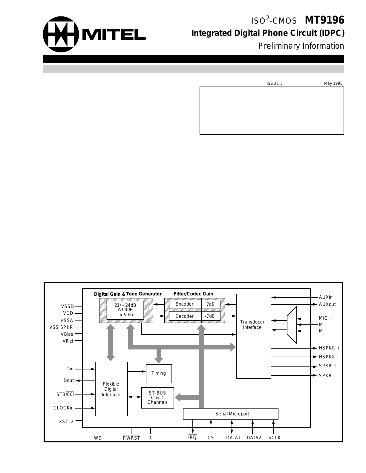
Figure 1 - Functional Block Diagram
AUXin
AUXout
MIC +
M M +
HSPKR +
HSPKR SPKR +
SPKR -
7-127
Page 2
MT9196 Preliminary Information
M-
M+
VBias
432
PWRST
VSSD
SCLK
DATA1
DATA2
5
6
IC
7
8
CS
9
10
11
12 13 14 15 16 17 18
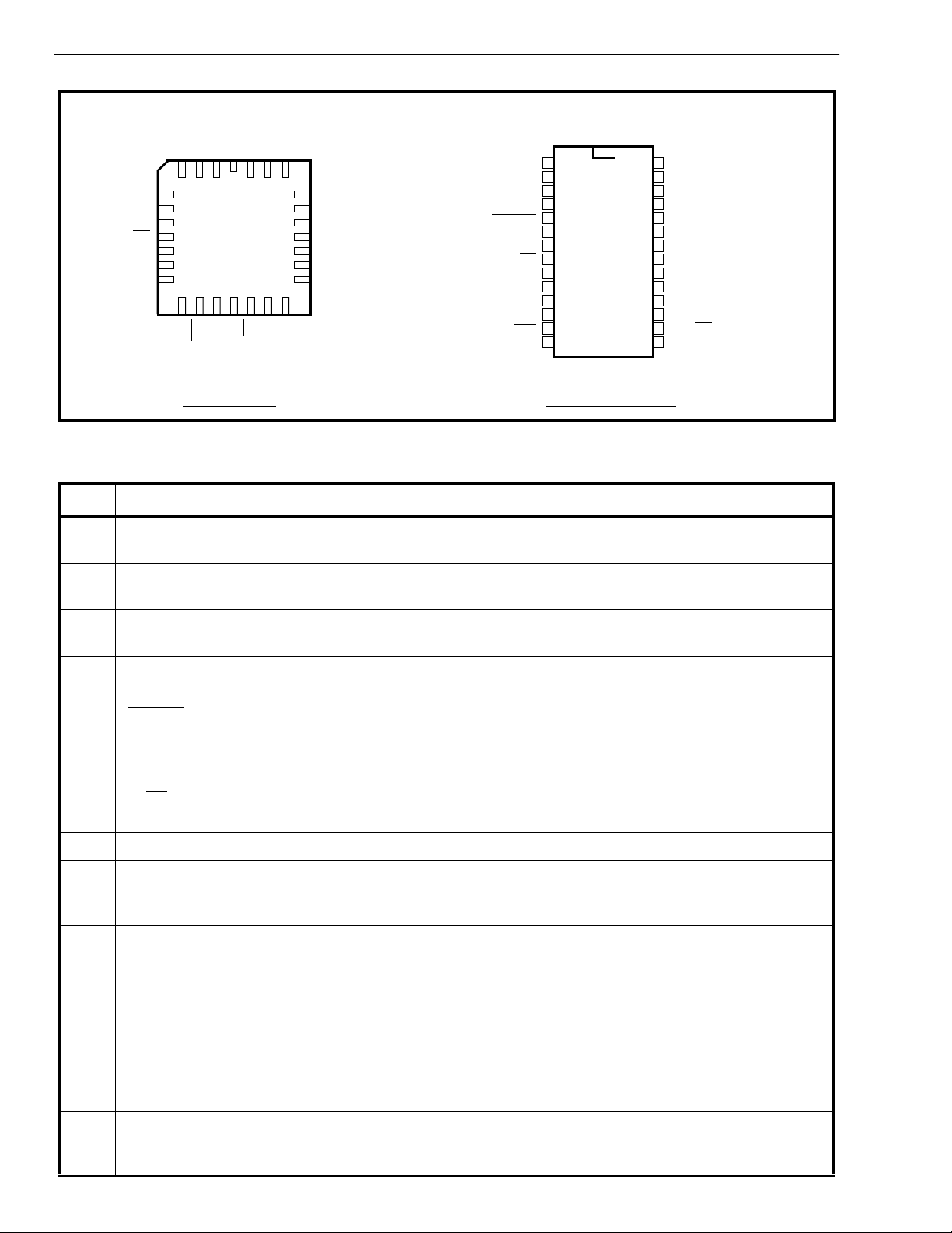
28 PIN PLCC 28 PIN SOIC/PDIP
Pin Description
VRef
WD
1
Din
IRQ
Dout
MIC+
VSSA
STB/F0i
CLOCKin
25
24
23
22
21
20
19
AUXin
262728
XSTAL2
AUXout
VSS SPKR
SPKR+
SPKRHSPKR+
HSPKRVDD
Figure 2 - Pin Connections
M-
M+
VBias
V
R
PWRST
IC
VSSD
CS
SCLK
DATA1
DATA2
WD
IRQ
Dout
1
2
3
4
f
e
5
6
7
8
9
10
11
12
13
14
28
27
26
25
24
23
22
21
20
19
18
17
16
15
VSSA
MIC+
AUXin
AUXout
VSS SPKR
SPKR+
SPKRHSPKR+
HSPKRVDD
XSTAL2
CLOCKin
STB/F0i
Din
Pin # Name Description
1M-Inverting Microphone (Input). Inverting input t o microphone amp lifier from the handset
microphone.
2M+Non-Inverting Microphone (Input). Non-inverting input to microphone amplifier from the
handset microphone.
3V
4V
Bias
Ref
5 PWRST
6ICInternal Co nne ctio n. Tie externally to V
7V
SSD
8CS
Bias Voltage (Output). (VDD/2) volts is available at this pin for biasing external am plif iers.
Connect 0.1 µF capacitor to V
SSA
.
Reference voltage for cod ec (Outpu t). Nominall y [ (VDD/2)-1.5] volts. Used internally.
Connect 0.1 µF capacitor to V
SSA
.
Power-up Reset (Input). CMOS compat ible inp ut with Schmit t Trigger (active low).
for normal operation.
SS
Digital Groun d. Nomi nally 0 volts.
Chip Select (Input). This input sign al is used to select the device for microport data
transfers. Active low. TTL level compatible.
9SCLKSerial Port Synch ronou s Clo ck (In put). Data clock for microport. TTL level compat ible.
10 DATA1 Bidirectional Serial Data. Port for microprocessor serial data transfer. In Motorola/National
mode of operatio n, this pin become s the data tra nsmi t pin only and data receive is
performed on the DATA2 pin. TTL level compatible input levels.
11 DATA2 Serial Data Receive. In Motorola/Natio nal mo de of operation, this pin is used for dat a
receive to the IDPC. In Intel mode, serial data transmit and rece ive are perform ed on the
DATA1 pin and DATA2 is disconnected. Input level TTL compatib le.
12 WD Watchdog (Output). Watchdog timer output. Active high.
13
14 D
IRQ
out
Interrupt Request (Ope n Drain Output). Low true inte rrupt output to microcontrolle r.
Data Output. A tri-state digital output for 8 bit wide channel dat a being sent to the Layer 1
device. Data is shifted out via this pin concurrent with the rising edge of BCL during the
timeslot define d by STB, or according to sta ndard ST-BUS timing.
15 D
Data Input. A digital input for 8 bit wide channel data received from the Layer 1 device.
in
Data is sampled on the falling edge of BCL during the timeslot defined by STB, or according
to standard ST-BUS timing. Input level is CMOS compatible.
7-128
Page 3

Preliminary Information MT9196
Pin Description (continued)
Pin # Name Description
16 STB/F0i Data Strobe/Frame Pulse (Input). For SSI mode this input determ ines the 8 bit timeslot
used by the device for both transmit and receive d ata. This a ctive high signa l has a
repetition rate of 8 kHz. Standard fram e pulse def init ions apply in ST-BUS mode. CMO S
level compatibl e input .
17 CLOCKin Clock Input. The clock provided to this input is used by the internal phone function s. In ST-
BUS mode this is t he C 4i
SSI-asynchronous mode this is an asynchronous 4 MHz Master Clock input.
18 XSTL2 Crystal Input (4.096 MHz). Used in conjunction with the CLOCKin pin to provide the master
clock signal via external crystal.
input. In SSI synchronous mode , this is the Bit Clock input. In
19 V
Positive Po wer Supply (Inp ut). Nominally 5 volts.
DD
20 HSPKR- Inverting Handset Speaker (Outpu t). Output to the handset speaker (balanced).
21 HSPKR+ Non-Inverting Handset Speaker (Output). O ut put to the handset speaker (balanced).
22 SPKR- In vertin g Speake r (Outpu t). Out put to the speakerphone speaker (balanced).
23 SPKR+ Non-I nver ting Speaker (Outpu t). Output to the speakerphone speaker (balanced).
24 V
25 AUX
SPKR Power Sup ply Rail for Speaker Dri ver. Nominally 0 Volts.
SS
Auxiliary Port (Outp ut). Access point to the D/A (analog) signals of the receive path as
out
well as to the various analog inputs.
26 AUX
Auxiliary Port (Input). An analog signal may be fed to the filter/codec transmit section and
in
various loopback paths via this pin. No external anti-aliasing is required.
27 MIC+ Non-inverting on-hoo k answ er back M icr op hon e (Input). Microphone amplif ier non-
inverting input pin.
28 V
SSA
Analog Gr ou nd (In pu t). Nominally 0 V.
7-129
Page 4

MT9196 Preliminary Information
Overview
The functional block diagram of Figure 1 depicts the
main operations performed by the MT9196 IDPC.
Each of these functional blocks will be described
individually in the sections to follow. This overview
will describe some of the end-user features which
may be implemented as a direct result of the level of
integration found within the IDPC.
The main feature required of a digital telephone is to
convert the digital Pulse Code Modulated (PCM)
information, be ing rece ived by the telephon e set, into
an analog electrical signal. This signal is then
applied to an appropriate audio transducer such that
the information is finally converted into intelligible
acoustic energy. The same is true of the reverse
direction where acoustic energy is converted first
into an electrical analog and then digitized (into
PCM) before being transmitted from the set. Along
the way if the signals can be manipulated, either in
the analog or the digital domains, other features
such as gain control and signal generation may be
added. Finally, most electro-acoustic transducers
(loudspeakers) require a large amount of power if
they are to develop an acoustic signal. The inclusion
of audio amplifiers to provide this power is required.
The IDPC features complete Analog/Digital and
Digital/Analog conversion of audio signals (Filter/
CODEC) and an analog interface to electro-acoustic
devic es (Tra n sd u ce r In te r f a ce ). Fu l l pro g ra m m a bil i ty
of the receive path and side-tone gains is available
to set comfortable listening levels for the user.
Transmit path gain control is available for setting
nominal transmit levels into the network. A digital,
anti-feedback circuit permits both the handset
microphone and the speaker-phone speaker to be
enabled at the same time for group listening
applications. This anti-feedback circuit limits the
total loop gain there by preventing a singing
condition from developing.
signalling protocol it may be necessary to use inband DTMF signalling to manipulate your personal
answering machine in order to retrieve messages.
Thus the locally generated tones must be of network
quality. The IDPC can generate the required tone
pairs as well as single tones to accommodate any inband signalling requirement.
Each of the programmable parameters within the
functional blocks is accessed through a serial
microcontroller port compatible with Intel MCS-51
Motorola SPI
Microwire
®
®
and National Semiconductor
specifications.
®
Functional Descripti on
In this section each of the functional blocks within
IDPC is described along with all of the associated
control/status bits. Each time a control/status bit(s) is
described it is followed by the address register
where it will be found. The reader is referred to the
section titled 'Register Summary' for a complete
listing of all address registers, the control/status bits
associated with each register and a definition of the
function of each control/status bit. The Register
Summary is useful for future reference of control/
status bits without the need to locate them in the text
of the functional descriptions.
Filter/CODEC
The Filter/CODEC block implements conversion of
the analog 3.3 kHz speech signals to/from the digital
domain compatible with 64 kb/s PCM B-Channels.
Selection of companding curves and digital code
assignment are register programmable. These are
CCITT G.711 A-law or µ-Law, with true-sign/
Alternate Digit Inversion or true-sign/Inverted
Magnitude coding, respectively. Optionally, signmagnitude coding may also be selected for
proprietary applications.
,
Signalling in digital telephone systems, behind the
PBX or standard ISDN applications, is handled on
the D-channel and generally does not require DTMF
tones. Locally generated tones, in the set, however,
can be used to provided “comfort tones” or “key
confirmation” to the user, similar to the familiar
DTMF tones generated by conventional phones
during initial call set-up. Also, as the network slowly
evolves from the dial pulse/DTMF methods to the DChannel protocols it is essential that the older
The Filter/CODEC block also implements transmit
and receive audio path gains in the analog domain.
These gains are in addition to the digital gain pad
section and provide an overall path gain resolution of
1.0dB. A programmable gain, voice side-tone path is
also included to provide proportional transmi t speech
feedback to the handset receiver. Figure 3 depicts
the nominal half-channel and side-tone gains for the
IDPC.
methods be available for backward compatibility. As
an example, once a call has been established (i.e.,
from your office to your home) using the D-Channel
Intel® and MCS-51® are registered trademarks of Intel Corporation
Motorola® and SPI® are registered trademarks of Motorola Corporation
National® and Microwire® are trademarks of National Semiconductor Corporation
7-130
Page 5
Preliminary Information MT9196
On PWRS T (pin 5) the Filter/CODEC defaults such
that the side-tone path, dial tone filter and 400 Hz
transmit filter are off, all programmable gains are set
to 0dB and CCITT µ-Law is selected. Further, the
Filter/CODEC is powered down due to the control
bits of the Path Control Registers (addresses 12h
and 13h) being reset.
The internal architecture is fully differential to provide
the best possible noise rejection as well as to allow a
wide dynamic range from a single 5 volt supply
design. This fully differential architecture is
continued into the Transducer Interface section to
provide full chip realization of these capabilities for
the handset and loudspeaker functions.
A reference voltage (V
), for the conversion
Ref
requirements of the CODEC section, and a bias
voltage (V
sections, are both generated on-chip. V
), for biasing the internal analog
Bias
Bias
is also
brought to an external pin so that it may be used for
biasing external gain plan setting amplifiers. A 0.1 µF
SERIAL
PORT
PCM
D
in
DIGITAL GAIN
& TONES
Receive
-24 to
+21 dB
(3dB steps)
DTMF,
Tone
Ringe r
FILTER/CODEC TRANSDUCER INTERFACE
Receive
Filter Gain
0 to -7 dB
(1 dB steps)
Side-ton e
-9.9 6 to
+9 96dB
(3.32 dB steps)
-11 dB
capacitor must be connected from V
ground at all times. Likewise, although V
to analog
Bias
may only
Ref
be used internally, a 0.1 µF capacitor from the V
pin to ground is required at all times. The analog
ground reference point for these two capacitors must
be physically the same point. To facilitate this the
V
Ref
and V
pins are situated on adjacent pins.
Bias
The transmit filter is designed to meet CCITT G.714
specifications. The nominal gain for this filter path is
0 dB (gain control = 0 dB). Gain control allows the
output signal to be increased up to 7 dB. An antialiasing filter is included. This is a second order
lowpass implementation with a corner frequency at
25 kHz. Attenuation is better than 32 dB at 256 kHz
and less than 0.01 dB within the passband.
An optional 400Hz high-pass function may be
included into the transmit path by enabling the Tfhp
bit in the Control Register 1 (address 0Eh). This
option allows the reduction of transmitted
background noise such as motor and fan noise.
Handset
Receiver
(150Ω)
75
75
Speakerphone
Speaker
(40Ω nominal)
34Ω min)
-6 dB
0/+8dB
+8 to -20dB
(4 dB steps)
RINGER
0 to -28 dB
(4 dB steps)
-6.1 dB or
-3.6 dB
Receiver
Driver
Speaker
Phone
Driver
0 dB
Auxiliary
Out
Driver
-12 dB
HSPKR +
HSPKR -
SPKR +
SPKR -
AUXout
Ref
PCM
D
out
-24 to
+21 dB
(3 dB steps)
Transmit
Digital Domain Analog Domain
Internal To Device External To Device
Transmit Filter
Gain
0 to +7 dB
(1 dB steps)
Trans-
mit
Gain
-0.37 dB
or 8.93 dB
Trans-
mit
Gain
6.37 dB
M
U
X
Figure 3 - Audio Gain Partitioning
5 dB
5 dB
AUXin
MIC+
M +
Transitter
microphone
M -
AUX input
H/F answer-
back mic
7-131
Page 6

MT9196 Preliminary Information
The receive filter is designed to meet CCITT G.714
specifications. The nominal gain for this filter path is
0 dB (gain control = 0dB). Gain control allows the
output signal to be attenuated up to 7 dB. Filter
response is peaked to compensate for the sinx/x
attenuation caused by the 8 kHz sampling rate.
The Rx filter function can be altered by enabling the
Dial EN control bit in Control Register 1 (address
0Eh). This causes another low-pass function to be
added with a 3 dB point at 1000 Hz. This function is
intended to improve the sound quality of digitally
generated dial tone received as PCM.
Side-tone is derived from the Tx filter before the LP/
HP filter section and is not subject to the gain control
of the Tx filter section. Side-tone is summed into the
receive handset transducer driver path after the Rx
filter gain control section so that Rx gain adjustment
will not affect side-tone levels. The side-tone path
may be enabled/disabled with the Voice sidetone bit
located in the Receive Path Control Register
(address 13h).
Transmit and receive filter gains are controlled by the
-TxFG2 and RxFG0-RxFG2 control bits,
TxFG
0
respectively. These are located in the FCODEC
Control Register 1 (address 0Ah). Transmit filter gain
is adjustable from 0 dB to +7 dB and receive filter
gain from 0 dB to -7 dB, both in 1 dB increments.
Side-tone filter gain is controlled by the STG
-ST G
0
control bits located in the FCODEC Control Register
2 (address 0Bh). Side-tone gain is adjustable from
-9.96 dB to +9.96 dB in 3.32 dB increments.
Companding law selection for the Filter /CODE C is
provided by the A/µ
companding control bit while
the coding scheme is controlled by the sign-mag/
CCITT
control bit. Both of these reside in Control
Register 2 (address 0Fh). Table 1 illustrates these
choices.
Code
+ Full Scale 1111 1111 1000 0000 1010 1010
+ Zero 1000 0000 1111 1111 1101 0101
-Zero
(quiet code)
- Full Scale 0111 1111 0000 0000 0010 1010
Sign/
Magnitude
0000 0000 0111 1111 0101 0101
CCITT (G.7 11)
µ-Law A-Law
Ta ble 1
Digital Gain and Tone Generation
The Digital gain and Tone generator block is located,
functionally, between the serial FDI port and the
Filter/CODEC block. Its main function is to provide
digital gain control of the transmit and receive audio
signals and to generate digital patterns for DTMF
and tone ringer signals.
Gain Control
Gain control is performed on linear code for both the
receive and the transmit PCM. Gain control is set via
the Digital Gain Control Register at address 19h.
Gain, in 3.0 dB increments, is available within a
range of +21.0 dB to -24 dB.
DTMF Ge nerat or
The digital DTMF circuit generates a dual sine-wave
pattern which may be routed into the receive path as
comfort tones or into the transmit path as network
signalling. In both cases the digitally generated
signal will undergo gain adjustment as programmed
into the transmit and receive gain control registers.
Gain control is assigned automatically as functions
are selected via the transmit and receive path control
registers.
The composite signal output level in the transmit
direction is -4 dBm0 (µ-Law) and -10 dBm0 (A-law)
2
with programmable gains at zero dB. Pre-twist of 2.0
dB is incorporated into the composite signal resulting
in a low tone output level of -8.12 dBm0 and a high
group level of -6.12dBm0 (for µ-Law, 6 dB lower for
A-Law). Note that these levels will be influenced by
the Anti-Howling circuit when it is enabled (see AntiHowling section for more details). DTMF side-tone
levels are se t to - 2 8 dB m0 from the gene ra to r circuit.
Other receive path gains must be included when
calculating the analog output signal levels.
Adjustments to these levels may be made by altering
the settings of the Gain Control register (address
19h).
The frequency of the low group tone is programmed
by writing an 8-bit coefficient into the Low Tone
Coefficient Register (address 1Ah) while the high
group tone frequency uses the 8-bit coefficient
programmed into the High Tone Coefficient Register
(address 1Bh). Both coefficients are determined by
the following equation:
The Filter/CODEC autonull circuit ensures that
transmit PCM will contain no more than ±1 bit of
offset due to i n te rn a l circuitry.
7-132
Frequency (in Hz) = 7.8125 x COEFF
Where COEFF is an integer between 0 and 255.
Frequency resolution is 7.8125 Hz in the range 0 to
1992 Hz.
Page 7
Preliminary Information MT9196
Low and high tones are enabled individually via the
LoEn and HiEN control bits (DTMF/Ringer Control
Register, address 18h). This not only provides
control over dual tone generation but also allows
single tone generation using either of the enable bits
and its associated coefficient register.
After programming and enabling the tone generators
as described, selection of transmit and/or receive
path destinations are carried out via the Path Control
Registers (see Path Control section). In addition
receive sidetone DTMF must be selected via the
DTMF StEN bit (DTMF/Tone ringer Register, address
18h) so that it replaces the received PCM in the Rx
Filter path.
Frequency
(Hz)
COEFF
Actual
Frequency%Deviation
697 59h 695.3 -.20%
770 63h 773.4 +.40%
852 6Dh 851.6 -.05%
941 79h 945.3 +.46%
1209 9Bh 1210.9 +.20%
1336 ABh 1335.9 .00%
1477 BDh 1476.6 -.03%
1633 D1h 1632.8 -.01%
Table 2 - DTMF Frequencies
DTMF Signal to distortion:
The sum of harmonic an d no is e po w er in t he freq uency band
from 50 Hz to 3500 Hz is typically more than 30 dB below the
power in th e ton e pair. All indiv idual ha rm on ic s ar e ty p ic al ly
more th an 4 0 d B b elow the l ev el o f the low group ton e.
Table 2 gives the standard DTMF frequencies, the
coefficient required to generate the closest
frequency, the actual frequency generated and the
percent deviation of the generated tone from the
nominal.
Tone Ring er
A dual frequency squarewave ringing signal may be
applied to the handsfree speaker driver to generate a
call alerting signal. To enable this mode the Ring En
bit (address 18h) must be set as well as the ringer
function to the loudspeaker via the Receive Path
Control Register (address 13h). Ring En is
independent of the DTMF enable control bits (see Lo
EN and Hi EN). Since both functions use the same
coefficient registers they are not usually enabled
simultaneously.
The digital tone generator uses the values
programmed into the low and high Tone Coefficient
Registers (addresses 1Ah and 1Bh) to generate two
different squa rewave freque n cie s.
Both coefficients are determined by the following
equation:
COEFF = [32000/Frequency (Hz)] - 1
where COEFF is an integer between 1 and 255. This
produces frequencies between 125 - 16000 Hz with
a non-linear resolution.
The ringer program switches between these two
frequencies at a 5 Hz or 10 Hz rate as selected by
the WR bit in the DTMF/Tone ringer register (address
18h).
Anti-Howl
IDPC includes an Anti-Howling circuit plus speaker
gain control circuit to allow for group listening
operation. Although this is the main function of the
circuit there are additional modes in which it may be
used as defined by the MS1 and MS0 control bits
(address 1Ch).
MS1
MS0 Op er ati o na l M o d e
0 0 Tx noise reduction (squelch)
0 1 Rx noise reduction (squelch)
1 0 switched loss group listening
(anti-howling)
1 1 Tx/R x s w itch e d los s
The circuit is enabled by setting the Anti-howl Enable
bit (address 1Ch) and selecting the required
operational mode (MS0 & MS1) as described.
For all modes of operation the switching levels and
inserted loss are programmed as follows.
Switching decisions are made by comparing either
the transmit or the receive signal level to threshold
levels stored in the High Threshold Register
(address 1Dh) and the Low Threshold Register
(address 1Eh). Threshold data is encoded in PCM
sign-magnitude format excluding the sign bit. For
example; THh0 - THh3 encode the PCM step
number while THh4 - THh6 encode the PCM chord
number for the high threshold. Similarily for the THl0
- THl6 bits of the low threshold. The difference
between the high and low threshold levels provides
the circuit with hysteresis to prevent uncontrolled
operation. The low level threshold must never be
programmed to a value higher than the one stored in
the high level threshold. If this occurs the circuit will
becom e unsta ble.
Loss is implemented, in the chosen path, by
subtracting the value set by the Pad0 - Pad3 control
bits from the appropriate gain value set by the RxG0
- RxG3 or TxG0 - TxG3 control bits (see Digital Gain
7-133
Page 8

MT9196 Preliminary Information
Register, address 19h). The minimum digital gain is
limited to -24 dB regardless of the mathematical
result of this operation. The path without loss reverts
to the gain value programmed into the Digital Gain
Register.
The magnitude of the switched loss defaults to 12 dB
on power up but c an be programmed to between 0
and 21 dB using the Pad0 - Pad2 control bits
(address 1Ch).
Pad2
0 0 0 0
0 0 1 3
0 1 0 6
0 1 1 9
1 0 0 12
1 0 1 15
1 1 0 18
1 1 1 21
Switched Loss fo r Group L isten ing (a nti-h owling)
Group listening is defined as a normal handset
conversation with received speech also directed to
the loudspeaker for third party observation. In this
mode, if the handset microphone is moved into close
proximity of the loudspeaker a feedback path will
occur resulting in a singing connection. To prevent
this the anti-howling circuit introduces a switched
loss into either the transmit or receive paths
dependent upon the transmit path speech activity.
Pad1 Pad0 Attenuation (dB)
comfortable group listening level after the handset
user has adjusted their listening level as required.
Since the anti-howling circuit has dynamic control
over the transmit and receive gain control registers,
it is recommended that this function be turned off
momentarily when DTMF tone generation is
required. This will ensure that the proper transmit
levels are attained.
Transmit Noise Reduction (squelch)
The transmit signal may be muted to eliminate
transmission of excessive background noise.
In this mode the signal level in the transmit path is
compared with the high level threshold stored at
address 1Dh. When the transmit signal level
exceeds this threshold no loss is inserted into the
transmit path. After exceeding the high level
threshold the transmit signal level is then compared
to a low level threshold stored at address 1Eh. When
the transmit signal level falls below this threshold the
transmit digital gain is reduced by the programmed
amount (Pad0-2) and comparison reverts back to the
high threshold level. The receive path gain is not
altered by transmit noise reduction.
Receive Noise Reduction (squelch)
Loss switching is determined by comparing the
signal level in the transmit path with the high level
threshold stored at address 1Dh. When the transmit
signal level exceeds this threshold the programmed
loss is s witched from th e tr a n sm it path to th e receive
path. Once switching has occurred the transmit
signal level is then compared to a low level threshold
stored at address 1Eh. When the transmit signal
level falls below this threshold the programmed loss
is switched from the received path back to the
transmit path and comparison reverts back to the
high threshold level.
Since the received digital gain control is used to set
the listening level of the received speech, for both
handset receiver and loudspeaker, it is necessary to
provide additional gain in the loudspeaker path so
that its receive level can be controlled independently
from the receiver out put. T he Gai n0 to Gain3 cont rol
bits (address 0B h) are used to boost the loudspeaker
output to a comfortable listening level for the third
parties in group listening. Generally the Gain3 bit
should be set to logic 1 in this mode. This increases
the gain programmed via the Gain0 - Gain2 bits by a
factor of 8 dB. In group listening a speaker gain
setting of 4 to 16 dB will be required to set a
The receive signal may be muted to eliminate
background noise resulting from a poor trunk
connection.
In this mode the signal level in the receive path is
compared with the high level threshold stored at
address 1Dh. When the receive signal level exceeds
this threshold no loss is inserted into the receive
path. After exceeding the high level threshold the
receive signal level is then compared to a low level
threshold stored at address 1Eh. When the receive
signal level falls below this threshold the receive
digital gain is reduced by the programmed amount
(Pad2-0) and comparison reverts back to the high
threshold level. The transmit path gain is not altered
by receive noise reduction.
Tx/Rx Switched Loss
In this mode the programmed switched loss is
inserted into either the transmit or receive path
dependent only upon activity in the receive path. If
receive path activity is above the programmed high
level threshold then the switched loss is inserted into
the transmit path. If receive path activity is below the
programmed low level threshold then the switched
loss is inserted into the receive path.
7-134
Page 9
Preliminary Information MT9196
This mode can be used to im plement a loudspeaking
function where the receive audio is routed to the
SPKR± pins and transmit audio is sourced from the
MIC+ pin. In this mode there is no algorithmic
cancellation of echo so it is recommended that this
switched loss program be used only in 4-wire
systems (i. e. , d i gital s e t to d i g ital s e t).
Transducer Interfaces
Four standard telephony transducer interfaces plus
an auxiliary I/O are provided by the IDPC. These are:
➧ The handset microphone inputs (transmitter),
pins M+/M- and the answerback microphone
input MIC+. The nominal transmit path gain
may be adjusted to either 6.0dB or 15.3dB.
Control of this gain is provided by the TxINC
control bit (Control register 2, address 0Fh).
This gain adjustment is in addition to the
programmable gain provided by the transmit
filter and Digital Gain circuit.
➧ The handset speaker outputs (receiver), pins
HSPKR+/HSPKR-.Thisinternallycompensated,
fully differential output driver is capable of
driving the load shown in Figure 4. The nominal
handset receive path gain may be adjusted to
either -12.1 dB or -9.6 dB. Control of this gain is
provided by the RxINC control bit (Control
register 2, address 0Fh). This gain adjustment
is in addition to the programmable gain
provided by the receive filter and Digital Gain
circuit.
➧ The loudspeaker outputs, pins SPKR+/SPKR-.
This internally compensated, fully differential
output driver is capable of directly driving 6.5v
p-p into a 40 ohm load.
➧ Auxiliary port path gains are:
AUXin to Dout
Din to AUXout
AUXin to AUXout
AUXin to HSPKR±
AUXin to SPKR±
11 dB
20.3 dB
-12 dB
-7.0 dB
-1.1 dB
1.4 dB
5.0 dB
TxINC=0
TxINC=1
RxINC=0
RxINC=1
Refer to the application diagrams of Figures 10 and
11 for typical connections to this analog I/O section.
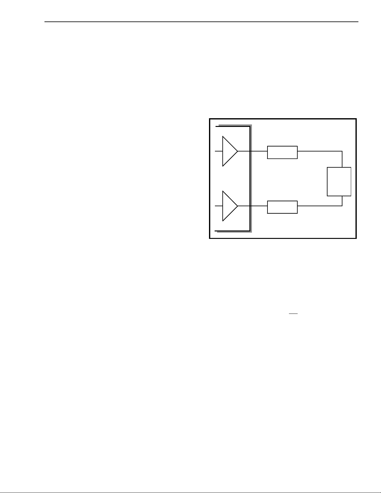
HSPKR +
75 Ω
IDPC
75 Ω
HSPKR -
150 ohm
load
(speaker)
Figure 4 - Handset Speaker Driver
Microport
The serial microport, compatible with Intel MCS-51
(mode 0), Motorola SPI (CPOL=0,CPHA=0) and
National Semiconductor Microwire specifications
provides access to all IDPC internal read and write
registers. This microport consists of a transmit/
receive data pin (DATA1), a receive data pin
(DATA2), a chip select pin (CS
) and a synchronous
data clock pin (SCLK).
➧ The Auxiliary Port provides an analog I/O, pins
AUXin and AUXout, for connection of external
equipment to the CODEC path as well as
allowing access to the speaker driver circuits.
➧ AUXin is a single ended high impedance
input (>10 Kohm). This is a self-biased
input with a maximum input range of
2.5vp-p. Signals should be capacitorcoupled to this input.
➧ AUXout is a buffered output capable of
driving 40 Kohm s//150 pF. Signals for this
output are derived from the receive path or
from the AUXin and transmit microphones.
The microport dynamically senses the state of the
serial clock each time chip select becomes active.
The device then automatically adjusts its internal
timing and pin configuration to conform to Intel or
Motorola/National requirements. If SCLK is high
during chip select activation then Intel mode 0 timing
is assumed. The DATA1 pin is defined as a bidirectional (transmit/receive) serial port and DATA2
is internally disconnected. If SCLK is low during chip
select activation then Motorola/National timing is
assumed. Motorola processor mode CPOL=0,
CPHA=0 must be used. DATA1 is defined as the data
transmit pin while DATA2 becomes the data receive
pin. Although the dual port Motorola controller
configuration usually supports full-duplex
communication, only half-duplex communication is
possible in IDPC. The micro must discard non-valid
data wh ich it cloc ks in dur ing a v alid w rit e tra nsfer to
7-135
Page 10
MT9196 Preliminary Information
IDPC. During a valid read transfer from IDPC data
simultaneously clocked out by the micro is ignored
by IDPC.
All data transfers through the microport are two-byte
transfers requiring the transmission of a Command/
Address byte followed by the data byte written or
read from the addressed register. CS
must remain
asserted fo r th e duration o f this two- byte transfer. As
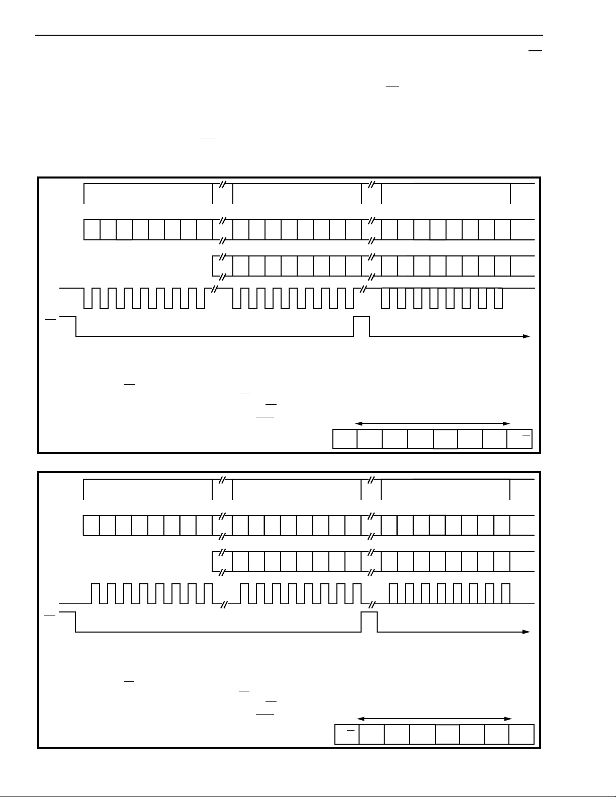
COMMAND/ADDRESS DATA INPUT/OUTPUT COMMAND/ADDRESS:
DATA 1
RECEIVE
DATA 1
TRANSMIT
SCLK
CS
➀ Delays due to internal processor timing which are transparent to IDPC.
② The IDPC:- latches received data on the rising edge of SCLK.
➂ The falling edge of CS
subsequent byte is always data until terminated via CS
➃ A new COMMAND/ADDRESS byte may be loaded only by CS
➄ The COMMAND/ADDRESS byte contains:
D0D1D2D3D4D5D6D
②
➂
- outputs transmit data on the falling edge of SCLK.
indicates that a COMMAND/ADDRESS byte will be transmitted from the microprocessor. The
➄
➀
D0D1D2D3D4D5D6D
7
D0D1D2D3D4D5D6D
returning high.
1 bit - Read/Write
5 bits - Addressing Data
2 bits - Unused
cycling high then low again.
shown in Figures 5 and 6 the falling edge of CS
indicates to the IDPC that a microport transfer is
about to begin. The first 8 clock cycles of SCLK after
the falling edge of CS
are always used to receive the
Command/Address byte from the microcontroller.
The Command/Address byte contains information
detailing whether the sec ond byte transfer will be a
read or a write operation and at what address. The
next 8 clock cycles are used to transfer the data byte
➀
7
7
➃
➂
D
7
XXA4A3A2A1A0R/W
➃
D0D1D2D3D4D5D6D
D0D1D2D3D4D5D6D
7
7
D
0
Figure 5 - Serial Port Relative Timing for Intel Mode 0
COMMAND/ADDRESS DATA INPUT/OUTPUT COMMAND/ADDRESS:
DATA 2
RECEIVE
DATA 1
TRANSMIT
SCLK
CS
➀Delays due to internal processor timing which are transparent to IDPC.
② The IDPC:- latches received data on the rising edge of SCLK.
➂ The falling edge of CS
subsequent byte is always data until terminated via CS
➃ A new COMMAND/ADDRESS byte may be loaded only by CS
➄ The COMMAND/ADDRESS byte contains:
D7D6D5D4D3D2D1D
②
➂
- outputs transmit data on the falling edge of SCLK.
indicates that a COMMAND/ADDRESS byte will be transmitted from the microprocessor. The
➄
➀
D7D6D5D4D3D2D1D
0
D7D6D5D4D3D2D1D
returning high.
1 bit - Read/Write
5 bits - Addressing Data
2 bits - Unused
cycling high then low again.
➀
0
0
➃
D
7
R/W XA4A3A2A1A0X
➃
D7D6D5D4D3D2D1D
D7D6D5D4D3D2D1D
➂
0
0
D
0
7-136
Figure 6 - Serial Port Relative Timing for Motorola Mode 00/National Microwire
Page 11

Preliminary Information MT9196
125 µ s
F0i
DSTi,
DST o
CHANNEL 0
D-channel
LSB first
for D-
Channel
CHANNEL 1
C-channel
CHANNEL 2
B1-channel
MSB first for C, B1- & B2-
Channels
CHANNEL 3
B2-channel
Figure 7 - ST-BUS Channel Assignment
between the IDPC and the microcontroller. At the
end of the two-byte transfer CS
to terminate the session. The rising edge of CS
is brought high again
will
tri-state the output driver of DATA 1 which will remain
tri-stated as long as CS
is high.
Intel processors utilize least significant bit first
transmission while Motorola/National processors
employ most significant bit first transmission. The
IDPC microport automatically accommodates these
two schemes for normal data bytes. However, to
ensure timely decoding of the R/W
and address
information, the Command/Address byte is defined
differently for Intel operation than it is for Motorola/
National operation. Refer to the relative timing
diagrams of Figures 5 and 6.
Receive data is sampled on the rising edge of SCLK
while transmit data is made available concurrent with
the falling edge of SCLK.
Detailed microport timing is shown in Figure 15.
Flexible Digital Interface
CHANNELS 4-31
Not Used
Quiet Co de
The FDI can be made to send quiet code to the
decoder and receive filter path by setting the
RxMUTE bit high. Likewise, the FDI will send quiet
code in t he transmit (DSTo) path when the TxMUTE
bit is high. Both of these control bits reside in Control
Register 1 at address 0Eh. When either of these bits
are low their respective paths function normally. The
-Zero entry of Table 1 is used for the quiet code
definition.
ST-BUS Mode
The ST-BUS consists of output (DSTo) and input
(DSTi) serial data streams, in FDI these are named
Dout and Din respectively, a synchronous clock input
signal CLOCKin (C4i
). These signals are direct connections to the
(F0i
), and a framing pulse input
corresponding pins of Mitel basic rate devices. Note
that in ST-BUS mode the XSTL2 pin is not used. The
CSL1 and CSL0 bits, as described in the SSI Mode
section, are also ignored since the data rate is fixed
for ST-BUS operation . However, the Async h/Synch
bit must be set to logic “ 0” fo r ST-BUS operation .
A serial link is required to transport data between the
IDPC and an external digital transmission device.
IDPC utilizes the ST-BUS architecture defined by
Mitel Semiconductor but also supports a strobed
data interface found on many standard CODEC
devices. This interface is commonly referred to as
Synchronous Serial Interface (SSI). The combination
of ST-BUS and SSI provides a Flexible Digital
Interface (FDI) capable of supporting all Mitel basic
rate transmission devices as well as many other
2B + D transceivers.
The required mode of operation is selected via the
ST-BUS/SSI
control bit (FDI Control Register,
address 10h). Pin definitions alter dependent upon
the operational mode selected, as described in the
following subsections as well as in the Pin
Description tables.
The data streams operate at 2048 kb/s and are Time
Division Multiplexed into 32 identical channels of 64
kb/s bandwidth. A frame pulse (a 244 nSec low going
pulse) is used to parse the continuous serial data
streams into the 32 channel TDM frames. Each
frame has a 125 µSecond period translating into an 8
kHz frame rate. A valid frame begins when F0i is
logic low coincident with a falling edge of C4i
to Figure 12 for detailed ST-BUS timing. C4i
. Refer
has a
frequency (4096 kHz) which is twice the data rate.
This clock is used to sample the data at the 3/4 bitcell position on DSTi and to make data available on
DSTo at the start of the bit-cell. C4i
is also used to
clock the ID PC inte r na l fu n cti o n s (i.e ., Filte r/CODEC,
Digital gain and tone generation) and to provide the
channel timing requirements.
The IDPC uses only the first four channels of the 32
channel frame. These channels are always defined,
7-137
Page 12

MT9196 Preliminary Information
beginning with Channel 0 after the frame pulse, as
shown in Figure 7 (ST-BUS channel assignments).
The first two (D & C) Channels are enabled for use
by the DEN and CEN bits respectively, (FDI Control
Register, address 10h). ISDN basic rate service
(2B+D) defines a 16kb/s signalling (D) Channel.
IDPC supports transparent access to this signalling
channel. ST-BUS basic rate transmission devices,
which may not employ a microport, provide access to
their int ernal control/status registers through the STBUS Control (C) Channel. IDPC supports microport
access to this C-Channel.
DEN - D-Channe l
In ST-BUS mode ac cess to the D -Channel ( transmit
and receive) data is provided through an 8-bit read/
write register (address 15h) D-Channel data is
accumulated in, or transmitted from this register at
the rate of 2 bits/frame for 16 kb/s operation (1 bit/
frame for 8 kb/s operation). Since the ST-BUS is
asynchronous, with respect to the microport, valid
access to this register is controlled through the use
of an interrupt (IRQ
enabled via the (DEn) bit.
) output. D-Channel access is
These di-bits are composed of the two D-Channel
bits received during each of frames n, n-1, n-2 and n-
3. Referrin g to Fig. 8a: di- bit I is mappe d from frame
n-3, di-bit II is mapped from frame n-2, di-bit III is
mapped from frame n-1 and di-bit IV is mapped from
frame n.
The D-Channel read register is not preset to any
particular value on power-up (PWRST
reset (RST).
(b) A microport write to Address 15hex will result in a
byte of data being loaded which is composed of four
di-bits (designated by roman numerals I, II, III, IV).
These di-bits are destined for the two D-Channel bits
transmitted during each of frames n+1, n+2, n+3,
n+4. Referring to Fig.8a: di-bit I is mapped to frame
n+1, di-bit II is mapped to frame n+2, di bit III is
mapped to frame n+3 and di bit IV is mapped to
frame n+4.
If no new data is written to address 15hex , the
current D-channel register contents will be
continuously re-transmitted. The D-Channel write
register is preset to all ones on power-up (PWRST
or softwa re r es e t ( RS T).
) or software
)
DEn:
When 1, ST-BUS D-channel dat a (1 or 2 bits/frame
depending on the state of the D8 bit) is shifted into/
out of the D-channel (READ/WRITE) register.
When 0, the receive D-channel data (READ) is still
shifted into the proper register while the DSTo Dchannel timeslot and IRQ
(default).
outputs are tri-stated
D8:
When 1, D-Channel data is shifted at the rate of 1 bit/
frame (8 kb /s ).
When 0, D-Channel data is shifted at the rate of 2
bits/frame (16 kb/s default ).
16 kb/s D-Channel operation is the default mode
which allows the microprocessor access to a full byte
of D-Channel information every fourth ST-BUS
frame. By arbitrarily assigning ST-BUS frame n as
the reference frame, during which the
microprocessor D-Channel read and write operations
are performed, then:
(a) A microport read of address 15 hex will result in a
byte of data being extracted which is composed of
four di-bits (designated by roman numerals I,II,III,IV).
An interrupt output is provided (IRQ
microprocessor access to the D-Channel register
during valid ST-BUS periods only. IRQ
every fourth (eighth in 8 kb/s mode) ST-BUS frame
at the beginning of the third (second in 8 kb/s mode)
ST-BUS bit cell period. The interrupt will be removed
following a microprocessor Read or Write of Address
15 hex or upon encountering the following frames’s
FP
input, whichever occurs first. To ensure DChannel data integrity, microport read/write access
to Address 15 hex must occur before the following
frame pulse. See Figure 8b for timing.
8 kb/s operation expands the interrupt to every eight
frames and processes data one-bit-per-frame. DChannel register data is mapped according to Figure
8c.
) to synchro nize
will occur
CEn - C-Chan nel
Channel 1 conveys the control/status information for
the layer 1 transceiver. C-Channel data is transferred
MSB first on the ST-BUS by IDPC. The full 64 kb/s
bandwidth is available and is assigned according to
which transceiver is being used. Consult the data
sheet for the selected transceiver for its C-Channel
bit definitions and order of bit transfer.
When CEN is high, data written to the C-Channel
register (address 14h) is transmitted, most
7-138
Page 13

Preliminary Information MT9196
IRQ
Micropo rt Rea d/Wri te A c cess
FP
DSTo/
DSTi
n-3 n-2 n-1 n n+1 n+2 n+3 n+4*
Di-bit Group
Receive
D-Channel
I
D0 D1
No preset value
II
D2 D3
D4
III
D5
* note that fram e n+4 is equ ival en t to frame n of the next cycle.
Figure 8a - D-Channel 16 kb/s Operation
FP
C4i
C2
Din
IRQ
D0
8 kb/s operation
D1
16 kb/s operation
IV
D6
D7
Di-bit Group
Transmit
D-Channel
t
if
D0 D1ID2
II
Power-up reset to 1111 1111
=500 nsec max
Microport Read/Write Access
D3
III
D4
D5
D6 D7
t
=500 nsec max
ir
R
pullup
Reset coincident with
Read/Write of Address 15 Hex
or next FP
, whichever occurs first
IV
= 10 k
FP
IRQ
Di-bit Group
Receive
D-Channel
Figure 8b - IRQ
n-7 n-6 n-5 n-4 n-3 n-2 n-1 n n+1
IID1IIID2IVD3VD4VID5VIID6VIII
I
D0
No preset value
Di-bit Group
Transmit
D-Channel
Timing Diagram
D7
Figure 8c - D-Channel 8 kb/s Operation
Microport Read/Write Access
I
D0
n+2
IID1IIID2IV
n+3
n+4
D3
Power-up reset to 1111 1111
n+5
VID5VIID6VIII
V
D4
n+6
n+7 n+8
D-Channel
D7
7-139
Page 14

MT9196 Preliminary Information
significant bit first, on DSTo. On power-up reset
(PWRST
) or software reset (RST, address 0Fh) all CChannel bits default to logic high. Receive CChannel data (DSTi) is always routed to the read
register regardless of this control bit's logic state.
When low, data transmission is halted and this
timeslot i s tri-stated o n D STo.
B1-Channe l and B 2-Cha nne l
Channels 2 and 3 are the B1 and B2 channels,
respectively. B-channel PCM associated with the
Digital Gain, Filter/CODEC and transducer audio
paths is selected on an independent basis for the
transmit and receive paths. For example, the
transmit path may use the B1 channel while the
receive path uses the B2 channel. Although not
normally required, this flexibility is allowed.
For ST-BUS mode the configuration of bits 0 to 3, at
address 12h, defines both the source of transmit
audio and the B-Channel destination. The
configuration of this register permits selection of only
one transmit B-Channel at a time. If no valid transmit
path has been selected, via the Transmit Path
Selection Register, for a particular B-Channel then
that timeslot output on DSTo is tri-stated.
The data strobe input STB determines the 8-bit
timeslot used by the device for both transmit and
receive data. This is an active high signal with an 8
kHz repetition rate.
SSI operation is separated into two categories based
upon the serial data rate. If the bit clock is 512 kHz or
greater then the bit clock is used directly by the
internal IDPC functions allowing synchronous
operation. In this case, the bit clock is connected
directly to the CLOCKin pin while XSTAL2 is left
unconnected. If the available bit clock rate is 128
kHz or 256 kHz then a 4096 kHz master clock is
required to derive clocks for the internal IDPC
functions. If this clock is available externally then it
may be applied directly to the CLOCKin pin. If a 4096
kHz clock is not available then provision is made to
connect a 4096 kHz crystal across the CLOCKin and
XSTAL2 pins as shown in Figure 9. The oscillator
circuit has been designed to require an external
feedback resistor and load capacitors. This
configuration allows normal ST-BUS operation and
synchronous SSI operation with clocks which are not
loaded by these extra components.
CLOCKin
33 pF
When a valid receive path has been selected, via the
Receive Path Selection Register (address 13h), the
active receive B-Channel is governed by the state of
the B2/B1 control bit in Control register 1 (address
0Eh ).
Refer to the Path Selection section for detailed
information.
SSI Mode
The SSI BUS consists of input and output serial data
streams named Din and Dout respectively, a Clock
input signal (CLOCKin), and a framing strobe input
(STB). A 4.096 MHz master clock, at CLOCKin, is
required for SSI operation if the bit clock is less than
512 kHz. The timing requirements for SSI are shown
in Figures 13 and 14.
In SSI mode the IDPC supports only B-Channel
operation. The internal C and D Channel registers
used in ST-BUS mode are not functional for SSI
operation. The control bit B2/B1
, as described in the
ST-BUS section, is ignored since the B-Channel
timeslot is def i ned by the input STB strobe. Hence, in
SSI mode transmit and receive B-Channel data are
always in the channel defined by the STB input.
100 kΩ
XSTL2
33 pF
4096 kHz
Nominal
Figure 9 - E xtern al Cryst al Circ uit
(for asynchronous operation)
Applications where the bit clock rate is below 512
kHz are designated as asynchronous. The IDPC will
generate and re-align its internal clocks to allow
operation when the external master and bit clocks
are asynchronous. In this case, the external bit
clock is not connected to the IDPC. Control bits
Asynch/Synch
, CSL1 and CSL0 in FDI Control
Register (address 10h) are used to program the bit
rates as shown in Table 3.
7-140
Page 15

Preliminary Information MT9196
filter, encoder and transmit gain are automatically
powered up and assigned as required. If transmit
Asynch/
Synch
1 0 0 128 4096
1 0 1 256 4096
0 0 0 512 512
0 0 1 1536 1536
0 1 0 2048 2048
0 1 1 4096 4096
For synchronous operation data is sampled, from
Din, on the falling edge of the bit clock during the
time slot defined by the STB input. Data is made
available, on Dout, on the rising edge of the bit clock
during the time slot defined by the STB input. Dout is
tri-stated at all times when STB is not true. If STB is
valid but no transmit path has been selected (via the
Transmit Path Control Register) then quiet code will
be transmitted on Dout during the valid strobe
period. There is no frame delay through the FDI
circuit for synchronous operation.
For asynchronous operation Dout and Din are as
defined for synchronous operation except that data
is transferred according to the itnernally generated
bit clock. Due to resynchronization circuitry activity,
the output jitter on Dout is nominally larger but will
not affect operation since the bit cell period at 128
kb/s and 256 kb/s is relatively large. There is a one
frame delay through the FDI circuit for asynchronous
operation. Refer to the specifications of Figures 13
and 14 for both synchronous and asynchronous SSI
timing.
CSL1 CSL0
Bit Clock
Rate (kHz)
Table 3
CLOCKin
(kHz)
mandatory
mandatory
tones is selected then the digital tone generator must
be programmed and enabled properly as described
in the Digital Tone Generator section. Note that
transmit tones may be enabled independently of the
receive path.
For ST-BUS mode the configuration of bit s 0 to 3, at
address 12h, defines both the source of transmit
audio and the B-Channel destination. The
configuration of this register permits selection of only
one transmit B-Channel at a time. For SSI mode only
the selections where bit 3 = 0 are allowed. This is
because the B-Channel timeslot is defined by the
input strobe at STB. If a selection where bit 3 = 1 is
made it will be treated the same as the condition
where B3 - B0 = all zero's.
All reserved configurations should not be used.
Receive
The receive path assignment (Receive Path Control
Register, address 13h) is different f rom the transmit
path assignment. In this case a particular analog
output port is assigned a source for its audio signal.
The receive filter audio path and the Auxiliary In
analog port are the available choices. This
configuration allows flexibility in assignment. Two
examples; the receive filter path can be assigned to
the handset receiver, for a standard handset
conversation, while permitting the loudspeaker to
announce a message originating from the Auxiliary
In port. Or perhaps the receive filter is assigned to
both the loudspeaker and the Auxiliary Out port. This
would allow a voice recorder or Facsimile machine,
connected to the AUXout port to be monitored over
the loudspeaker.
Path Selection
Transmit and receive audio paths are independently
programmed through their respective Path Control
Registers at addresses 12h and 13h. Individual
audio path circuit blocks are powered up only as they
are required to satisfy the programmed values in the
path control registers. More detail is provided in the
Power-up/down Reset section.
Transmit
Transmit audio path configuration (Path Control
Register, address 12h) is simply a matter of
assigning one of the three analog signal inputs, or
the digita l tone g ener ator, to the requ ired transm it BChannel. Intermediate functions such as the transmit
The receive filter path itself has two possible signal
sources, PCM from the Din port or synthesized
tones, from the digital tone generator. In both cases
receive digital gain is assigned automatically. The
Receive Path Control Register combin es all of these
choices into simple output port assignments.
In ST-BUS mode receive PCM from the Din port
must be selected from either the B1 or the B2
channel. Control Bit B2/B1 in Control Register 1
(address 0Eh) is used to define the active receive BChannel. In SSI mode the active PCM channel is
automatically defined by the STB input signal.
7-141
Page 16

MT9196 Preliminary Information
Sidetone
➧The receive output drive transducers. All
A voice sidetone path provides proportional transmit
signal summing into the receive handset transducer
driver. Details are provided in the Filter/CODEC
section.
Watchdog
transducer output drivers are powered down
forcing the output signals into tri-state. Output
drivers (handset, handsfree-speaker, AUXout)
are powered up/down individually as required
by the state of the programmed bits in the
Receive Path Cont rol Register (address 13h)
To maintain program integrity an on-chip watchdog
timer is provided for connection to the
microcontroller reset pin. The watchdog output WD
goes high while the I DPC is held in reset via PWRST
Release of PWRST
immediately and will also start the watchdog timer.
The watchdog timer is clocked on the falling edge of
STB/F0i
for operation. Note that in SSI mode, if STB
disappears the watchdog will stop clocking. This will
not harm processor operation but there is no longer
any protection provided.
If the watchdog reset word is written to the watchdog
register (address 11h) after PWRST
before the timeout period (T=512 mSec) expires, a
reset of the timer results and WD will remain low.
Thereafter, if the reset word is loaded correctly at
intervals less than 'T' then WD will continue low. The
first break from this routine, in which the watchdog
register is not written to within the correct interval or
it is written to with incorrect data, will result in a high
going WD output after the current interval 'T' expires.
WD will then toggle at this rate until the watchdog
register is again written to correctly.
5-BIT WATCHDOG RESET WORD
x=don’t c are
Power-up/down & PWRST/Software Reset
While the IDPC is held in PWRST
or functionality is possible. While in software reset
(RST=1, address 0Fh) only the microport and
watchdog a re functio nal. Softw are rese t can o nly be
removed by writing RST logic low or by the PWRST
pin.
After Power-up reset (PWRST
(RST) all control bits assume their default states;
µ-Law functionality, usually 0 dB programmable
gains and all sections of IDPC, except the microport
and watchdog, into powered down states. This is the
low power, stand-by condition. This includes:
and requires only this input , along wit h VDD,
B7 B6 B5 B4 B3 B2 B1 B0
XXX01010
will cause WD to return low
is released, but
no device control
) or software reset
➧ The transmit and receive filt ers and CODEC. All
clocks for this circuit block are disabled. The
complete section is automatically powered up
.
as required by the programmed bits in the
Transmit and Receive Path Control registers
(addresses 12h and 13h). Whenever all path
control selections are off this section is
powered down. The CODEC and transmit/
receive filters cannot be powered up
individually.
➧ The VRef and VBias circuits. Reference and
Bias voltage drivers are tri-stated during power
down causing the voltage at the pins to float.
This circuit block is automatically powered up/
down as it is required by either the Filter/
CODEC or the transducer driver circuits.
Whenever all path control selections are off this
section is powered down. If the AUXin path to
(any combination of the) output transducer
drivers is selected then the VRef/VBias circuit
is powered up but the Filter/CODEC circuit is
not.
➧ The FDI and oscillator circuits. After PWRST
the device assumes SSI operation with Dout tristated while there is no strobe active on STB. If
a valid strobe is supplied to STB, then Dout will
be active, during the defined channel, supplying
quiet code as defined in Table 1. If the device
is switched to ST-BUS operation following
PWRST
until an active transmit channel is programmed.
As well, following PWRST
is disabled and all timing for the IDPC
functional blocks is halted. A clock signal
applied to the MCL pin is prevented from
entering further into the IDPC when the Asynch/
Synch
To power up the FDI and oscillator circuits the
PD bit of Control Register 1 (address 0Eh) must
be cleared.
To attain complete power-down from a normal
operating condition, write all “0s” to the
Transmit and Receive Path Control Registers
(address 12h and 13h), set PD to logic 1 at
address 0Eh, and Asynch/Synch
address 10h.
, the entire Dou t stream will be tr i-stated
, the oscilla tor circuit
bit is logic “1”.
to logic 1 at
,
7-142
Page 17

Preliminary Information MT9196
IDPC Register Map
00
•
•
•
09
RESERVED
0A - RxFG
0B Gain3 Gai n2 Gain1 Gain0 - STG
RxFG1RxFG
2
-TxFG
0
2
2
TxFG
STG
TxFG
1
1
0C ---------------------------------------RESERVED---------------------------------0D ---------------------------------------RESERVED----------------------------------
0E PD Tf hp DialEn - - B2/ B1
0F RST - A/µ
Smag/
RxINC TxINC - - Control Register 2
RxMute TxMute Control Register 1
CCITT
10 - ST-BUS/
SSI
11 - - - W
12 - - - - b
13 b
14 b
15 D
7
7
7
b
6
b
6
D
6
CEN DEN D
4
b
5
b
5
D
5
b
4
b
4
D
4
W
8
Asynch/
CSL
1
Synch
3
3
b
3
b
3
D
3
W
2
b
2
b
2
b
2
D
2
W
1
b
1
b
1
b
1
D
1
16 ---------------------------------------RESERVED---------------------------------17 - - Loop
Loop
2
1
- - - - Loopb a ck Register
STG
CSL
W
b
b
b
D
FCodec Control 1
0
FCodec Control 2
0
0
0
0
0
0
0
FDI Control
Tx Path Control
Rx Path Control
C-Channel Register
D-Channel Register
Watchdog
18 HiE N LoEn DTMF
StEn
19 TxG
1A L
1B H
7
7
TxG
3
L
6
H
6
TxG
2
L
5
H
5
1C Enable - MS
1D - TH
1E - TH
h6
l6
TH
TH
h5
1F
•
•
•
3F
Ring En - - - WR DTMF/Tone Ringer
TxG
1
L
H
MS
1
TH
TH
l5
RxG
0
4
4
0
h4
l4
L
3
H
-Pad
TH
TH
RxG
3
L
2
3
h3
l3
H
TH
TH
2
h2
2
2
l2
RxG
L
H
Pad
TH
TH
RxG
1
1
1
1
h1
l1
L
H
Pad
TH
TH
0
0
0
0
h0
l0
Digital Gain
Low Tone Coeff
High Tone Coeff
Anti-Howl Control
High Threshold
Low Threshold
RESERVED
7-143
Page 18

MT9196 Preliminary Information
Register Summary
ADDRESSES = 00h to 09h ARE RESERVE D
Filter Codec Contr ol Regis ter 1 ADDRESS = 0Ah WRITE/REA D VERIFY
Power Reset Value
RxFG2RxFG1RxFG
-
-
0
TxFG2TxFG1TxFG
0
76543210
X000 X000
Receive Gain
Setting (dB)
(default) 0
-1
-2
-3
-4
-5
-6
-7
RxFG
0
0
0
0
1
1
1
1
RxFGn = Receive Filter Gain n TxFGn = Transmit Filter Gain n
RxFG
2
0
0
1
1
0
0
1
1
RxFG
1
0
0
1
0
1
0
1
0
1
Transmit Gain
Setting (dB)
(default) 0
1
2
3
4
5
6
7
TxFG
0
0
0
0
1
1
1
1
TxFG
2
0
0
1
1
0
0
1
1
TxFG
1
0
0
1
0
1
0
1
0
1
Filter Codec Contr ol Regis ter 2 ADDRESS = 0Bh WRITE/REA D VERIFY
Power Reset Value
Gain3 Gain2 Gain1 Gain0 STG2STG1STG
-
0
0010 X000
76543210
Speaker Gain (dB)
Gain3 = 1 Gain3 = 0
16
12
8
4
0
-4
-8
-12
8
4
0
-4
-8
-12
-16
-20
Gain2 Gain1 Gain0
0
0
0
0
1
1
1
1
0
0
1
1
0
0
1
1
0
1
0
1
0
1
0
1
Side-tone Gain
Setting (dB)
(default) OFF
Note: Bits marked "-" are reserved bits and should be written with logic "0".
7-144
-9.96
-6.64
-3.32
0
3.32
6.64
9.96
STG
0
0
0
0
1
1
1
1
2
STG
0
0
1
1
0
0
1
1
STGn = Side-tone Gain n
STG
1
0
0
1
0
1
0
1
0
1
ADDRES S = 0 C h RE SERVED
Page 19

Preliminary Information MT9196
ADDRES S = 0 D h RE SERVED
Control Reg ister 1 ADDRESS = 0Eh WRITE/REA D VERIFY
Power Reset Value
PD Tfhp DialEN - B2/B1 RxMute TxMute
-
76543210
PD When high, th e crys tal os c ill ator an d FDI block s ar e pow ere d do wn. When low, the oscillator and FDI circuits are active.
Tfhp When High, an add itional highpass fu nction (p assband beg inning at 400 Hz) is inserte d into th e transmit pat h. When
DialEN When high, a first order lowpa ss filter is inserted into the receive pa th (3dB = 1kHz). When low, this lowpas s filter is
B2/B1
RxMUTE Whe n high the received PCM stream is interrupted and repla ced with quiet code; thus forcing the receive path into a
TxMUTE When h igh the transmi t PCM stream i s interrupted and replaced wit h quiet code ; thus forcing the output code int o a
low, this highpass filter is disabled.
disabled.
When high, the receive Filter/CODEC operates on the B2-Ch annel. When low, the re ceive Filter/CODE C operates on
the B1-Channel. This control bit has significance only for ST-BUS operation and is ignored for SSI operation.
mute state. When low the full recei ve path functi ons norm all y.
mute state (only the o utput code is mute d, the transmi t microphone and transmit F ilter/CODEC are still functional) .
When low the full transmit path functions normally.
100X X000
Control Reg ister 2 ADDRESS = 0Fh WRITE/READ VERIFY
Power Reset Value
0X00 00XX
RST
-
A/µ
Smag/
CCITT
RxINC
TxINC
--
76543210
RST When high, a software reset occur s performing th e same function as the hardware reset (PWRST) except that the
A/µ
Smag/CCITT
RxINC When high, the receiver driver nominal gain is se t at -9.6dB. When low , this driver nom inal ga in is set at -12.1dB.
TxINC When high, the transmit amplifier nominal gain is set at 15.3dB. When low, this amplifier nominal gain is set at 6.0dB.
microport and watchdog circuitry are not affected. A software reset can be removed only by writing this bit low or by a
PWRST
. When low, the reset condition is removed.
When high, A-Law (d e)coding is selected for the Filter/CODEC a nd DTMF generator circuits. When low, µ-Law
(de)coding is selected for these circuits.
When high, sign-magnitude code assignment is selected for the CODEC input/output. When low, CCITT code
assignment is selected for the CODEC input/output; true sign, inverted magnitude (µ-Law) or true sign, alternate digit
inversion (A-Law).
Note: Bits marked "-" are reserved bits and should be written with logic "0".
7-145
Page 20

MT9196 Preliminary Information
FDI Control Register ADDRESS = 10h WRITE/READ VER IFY
ST-BUS/
-
SSI
CEN DEN
D8
Asynch/
Synch
CSL1CSL
0
Power Reset Value
X000 0000
76543210
ST-BUS/SSI When hi gh, the FDI port ope rates in ST-BUS mode. Wh en low, the FDI operate s in SSI mode.
CEN When high, data written into the C-Channel register (address 14h) are transmi tted during channel 1 on DSTo .
DEN W hen high, d ata writte n into the D-Cha nnel Reg ister (ad dress 15h ) are transmi tted duri ng chan nel 0 on DSTo .
D8 W hen high , the D-Channel operat es at 8 kb/s.
Asynch/Synch
CSL
,CSL
1
0
Asynch/Synch
When low, t he channel 1 t imeslot is tri-sta ted on DSTo. Channel 1 da ta received on D STi is read vi a the CChannel register (a dd ress 14h) re gardless of the state of CEN. This con tro l bit has sign ifican ce only for ST-BUS
operation and is ignore d for SSI operation.
When low, t he channel 0 t imeslot is tri-sta ted on DSTo. Channel 0 da ta received on D STi is read vi a the DChannel regi ster reg ardless o f the stat e of DEN. T his contr ol bit has sig nifican ce only for ST-BUS m ode and is
ignored for SSI operation.
When low, the D-Channel operates at 16 kb/s default.
, Control bits Asynch/Synch, CSL1 and CSL0 are used to program the data clock (BCL) bit ra tes as shown in the
following table (CSL1 and CSL0 are ignored in ST-BUS mode):
CSL
1 0 0 128 4096 mandatory
1 0 1 256 4096 mandatory
000 512 512
0 0 1 1536 1536
0 1 0 2048 2048
0 1 1 4096 4096
CSL
1
0
Bit Clock Rate (kHz) CLOCKin (kHz)
Note: Asynch/Synch must be set low for ST-BUS operation
Watchdog Register ADDRESS = 11h WRITE
Power Reset Value
---0 010
1
XXXX XXXX
76543210
Note: Bits marked "-" are reserved bits and should be written with logic "0".
7-146
Page 21

Preliminary Information MT9196
Transmit Path Control Register ADDRESS = 12h WRITE/RE AD VER IFY
Power Reset Value
---
b1 b0b3- b2
76543210
Control bits b0 to b3 are used to configure the transmit path and select the transmit source. Note that for SSI mode all selections where
b3 = 1 are not used and are interpreted as b0 - b3 = 0 (i.e., transmit path off).
XXXX 0000
Destination
B1 0
B2 1
b
0
0
0
0
0
0
0
1
1
1
1
1
1
1
b
3
2
0
0
0
0
1
1
1
1
0
0
0
0
1
1
1
1
Source Programming
b
0
0
1
1
0
0
1
1
0
0
1
1
0
0
1
1
b
1
0
B
0
1
0
1
0
1
0
1
0
1
0
1
0
1
0
1
& B2 Off
1
Handset mic (M + /M -)
Handsfree mic (MIC +)
AUXin
Tx tones
Reserved
Reserved
Reserved
Reserved
Handset mic (M + /M -)
Handsfree ic (MIC +)
AUXin
Tx Tones
Reserved
Reserved
Reserved
Receive Path Contro l Register ADDRESS = 13h WRITE/READ VER IFY
Power Reset Value
b7 b5 b4 b1 b0b3b6 b2
000 0 00 00
76543210
Control bits b0 t o b7 are used to assign a sig nal source indi vidually to each recei ve pat h outpu t. In ad dition tran smit t o recei ve voice
sidetone path control is included.
Destination Source Programming
Handset Speaker b
Handsfree Speaker b
Aux out b
Voice Sidetone b
0
0
1
1
0
0
1
1
0
0
0
0
1
1
1
1
01Voice sidetone path disabled
b
1
3
6
7
0
0
1
0
1
b
2
0
1
0
1
b
5
0
0
1
1
0
0
1
1
Off
Rx Filter
AUXin
Reserved
Off
Rx Filter
AUXin
Reserved
b
4
0
1
0
1
0
1
0
1
Voice sidetone path enabled
Off
Rx Filter
Reserved
AUXin
Handset mic (M+ /M -)
Handsfree mic (MIC +)
Reserved
Reserved
Note: Bits marked "-" are reserved bits and should be written with logic "0".
7-147
Page 22

MT9196 Preliminary Information
C-Channel Register ADDRESS = 14h WRITE/READ
Power Reset Value
B7 B6 B5 B4 B2 B1 B0B3
76543210
Micro-port access to the ST-BUS C-Channel information
D-Channel Register ADDRESS = 15h WRITE/READ
D7
D6 D5 D4 D2 D1 D0
D3
76543210
ADDRESS = 1 6 h RESERVED
111 1 11 11
Power Reset Value
1111 1111
Loopback Regi ster ADDRESS = 17h WRITE/READ VERI FY
Power Reset Value
--
Loop2 Loop1 ---
-
XX00 XXXX
76543210
Loop1 When h igh, the sel ecte d B-cha nn el in ST -BUS m o de (i. e. , B2/B1 and Tra nsm it an d Receive Path selections) or the strob ed
Loop2 When high, Loop1 is invoked with the transmit and receive digital gain adjustment being included. This loopback should only
Notes: 1) do not enable Loop1 and Loop2 si multaneously.
B-channel in SSI mode is looped back from Din to Dout through the FDI block. The C & D channels (ST-BUS mode) are not
looped back. When low, the device operates normally.
be used if PCM resides in the B-channel. If a data pattern is being looped back then use Loop1 or use Loop2 after ensuring
that the transmit and receive digital gain registers are set to 0dB (address 19h). When low, the device operates normally.
2) both loo pback mod es add an extra fram e delay to the data transmi ssi on .
3) ensure that all other bits of address 17h are written logic low when accessing this register.
Note: Bits marked "-" are reserved bits and should be written with logic "0".
7-148
Page 23

Preliminary Information MT9196
DTMF/Tone Ringer Control Register ADDRESS = 18h WRITE/READ VERIFY
Power Reset Value
0000 XXX0
HiEN LoEN
DTMF Ring
St EN
En
-
--WR
76543210
HiEN, LoEN When high, the progra mme d tone, for the respect ive high or low group , is generat ed. When low , tone generatio n is
DTMF St EN When high, pro grammed DTMF is muxed into the recei ve path replacing the recei ve PCM signal. When low, the
Ring EN When high, the tone ringer ge nerat or is enab le d using the coefficients at addresses 1Ah and 1Bh as well as the WR
WR When high, the tone ringer circuit will toggle between the two programmed frequencies at a 5 Hz rate. When low, the
disabled for the respective low or high group.
receive path functio n s normall y.
control bit. Fo r the ringer tone to be appl ied to the loudspeaker th e proper path must b e selected via the Recei ve
Path Control Register (address 13h). When low, the ring generator circuit is disabled.
tone ringer warb le rate is 10Hz .
Digital Gain Register ADDRESS = 19h WRITE/READ VER IFY
Power Reset Value
TxG
TxG2TxG1TxG
3
RxG
0
RxG
3
RxG
2
RxG
1
0
100 0 10 00
76543210
Transmit (TxG
RxG
0
0
0
0
0
0
0
0
1
1
1
1
1
1
1
1
) and receive (RxG
3-0
RxG
3
0
0
0
0
1
1
1
1
0
0
0
0
1
1
1
1
) control bits for programming gain in 3 dB increments.
3-0
RxG
2
0
0
1
1
0
0
1
1
0
0
1
1
0
0
1
1
RxG
1
0
1
0
1
0
1
0
1
0
1
0
1
0
1
0
1
Gain Adjustment (dB) TxG
0
-24
-21
-18
-15
-12
-9
-6
-3
0
+3
+6
+9
+12
+15
+18
+21
3
0
0
0
0
0
0
0
0
1
1
1
1
1
1
1
1
TxG
2
0
0
0
0
1
1
1
1
0
0
0
0
1
1
1
1
TxG
0
0
1
1
0
0
1
1
0
0
1
1
0
0
1
1
1
TxG
0
0
1
0
1
0
1
0
1
0
1
0
1
0
1
0
1
Low Tone Coefficient Register ADDRESS = 1Ah WRITE/READ VERIFY
Power Reset Value
L7 L6 L5 L4 L3 L2 L1 L0
000 0 00 00
76543210
The frequency of the low group tone is programmed by writing an 8-bit hexadecimal coefficient at this address according to the following
equation:
Frequency (in Hz) = 7.8125 x COEFF
Where the hexadecimal COEFF is conve rted into a decimal integer bet ween 0 and 255. Frequency resolu tion is 7.8125Hz in the range
0 to 1992 Hz.
Note: Bits marked "-" are reserved bits and should be written with logic "0".
7-149
Page 24

MT9196 Preliminary Information
High Tone Coefficient Register ADDRESS = 1Bh WRITE/READ VERIFY
H7 H6 H5 H4 H3 H2 H1 H0
76543210
The frequency of the high group tone is programmed by writing an 8-bit hexadecimal coefficient at this address according to the
following equation:
Frequency (in Hz) = 7.8125 x COEFF
Where the hexadecimal COEFF is conve rted into a decimal integer bet ween 0 and 255. Frequency resolu tion is 7.8125Hz in the range
0 to 1992 Hz.
Power Reset Value
0000 0000
Anti-Howl Control Register
Enable - MS1 MS0 Pad2 Pad1 Pad0
-
ADDRESS = 1Ch WRITE/READ VERI FY
Power Reset Value
0X10 X100
76543210
Enable When high, the anti-howling circuit is enabled. When low, the anti-howling circuit is disabled.
MS1, MS0 Encode the operat ional mode of t he anti-howling circu it as follows. Details of each mode are f ound in the f unctional
Pad2-0 Three bits e nco ding th e a ttenu a tio n depth wh ich will be switche d i nt o the tra nsm it or receive p aths b y t he a nti-howling
description of the anti-howling circuit.
MS1 MS0 Operational Mode
0 0 Transmit Noise Squelch
0 1 Rece ive Noi se Sque lch
1 0 Anti-howling for group listening
1 1 Tx/Rx Switched Loss
circuit. Note that 12 dB is the default value.
Pad2 Pad1 Pad0 At tenu ati on (dB)
000 0
001 3
010 6
011 9
100 12
101 15
110 18
111 21
High Threshold Register ADDRESS = 1Dh WRITE/REA D VERI FY
THh6 THh5 THh4 THh3 THh2 THh1 THh0
-
Power Reset Value
X011 0000
76543210
THh6-0 Seven bits encoding the magnitude of the high threshold level. Encoding is in PCM sign-magnitude excluding the sign bit.
THh0 - T Hh3 e ncode the step number wh ile THh 4 - T Hh6 e ncode the cho rd n um be r. Th e defa ul t setting of 'X0 11 000 0'
encodes chord 3 step 0. The differe nce be twee n the high an d low thresho ld s defin es the hysteresis for anti-ho wling.
Low Threshold Register ADDRESS = 1Eh WRITE/READ VERIFY
THI6 THI5 THI4 THI3 THI2 THI1 THI0
-
Power Reset Value
X001 0100
76543210
THl6-0 Seve n bits en cod ing th e magnit ude o f the low thre shol d level . Enco ding is in PCM sign -mag nit ude exclu di ng the si gn bit .
THl0 - THl3 encode the step nu mber while THl4 - THl6 encode the chord number. The defa ult setting of 'X0 01 0100'
encodes chord 1 step 4. The differe nce be twee n the high an d low thresho ld s defin es the hysteresis for anti-ho wling.
ADDRESS ES 1Fh to 3Fh are RESERVED
Note: Bits marked "-" are reserved bits and should be written with logic "0".
7-150
Page 25

Preliminary Information MT9196
Applications
330 Ω
+5V
0.1 µF
0.1 µF
511 Ω
511 Ω
+
10 µF
Electret
+
Microphone
Typical External Gain for Handse t
AV= 5 - 10
Typical External Gain for MIC
AV= 20 - 25
R
Av = 1 + 2R
R
+
100K
VBias
T
T
100K
-
+
MOTOROLA
Controller
RESET
INTEL
MCS-51
or
SPI
Micro-
+5V
CS
SCLK
DATA1
DATA2
DATA2 Mo to rol a
Mode only
WD
IRQ
DC to DC
CONVERTER
0.1 µF
0.1 µF
+5V
VBias
4 3 2 1 28 27 26
5
6
7
8
9
10
11
12 13 14 15 16 17 18
DSTo DSTi
IDPC
F0
R
From Auxiliary
Audio Source
25
24
23
22
21
20
19
+
-
0.1µF
+5V
VBias
T
0.1 µF
To Auxiliary Audio Source
75Ω
75Ω
330Ω
+5V
1K
40Ω nom.
34Ω min.
+
10µF
Electret
+
Microphone
150Ω
Twisted Pair
Lin
Z
Lout
T
MT8972
DNIC
10.24 MHz
C4
Figure 10 - ST-BUS Application Circuit with MT8972 (DNIC)
7-151
Page 26

MT9196 Preliminary Information
AAAA
AAAA
A
AAAA
AAAA
A
330 Ω
Typical Extern al Gain for Handse t
AV= 5 - 10
Typical Extern al Gain for MIC
AV= 20 - 25
R
Av = 1 + 2R
R
+
100K
VBias
T
T
100K
-
+
0.1 µF
0.1 µF
+5V
511 Ω
511 Ω
+
10 µF
Electret
+
Microphone
MOTOROLA
Controller
RESET
INTEL
MCS-51
or
SPI
Micro-
Twisted Pair
0.1 µF
0.1 µF
+5V
CS
SCLK
DATA1
DATA2
DATA2 Motorola
Mode only
WD
IRQ
Layer 1
Transceiver
using
SSI
Synch
Mode
VBias
4 3 2 1 28 27 26
5
6
7
8
IDPC
9
10
11
12 13 14 15 16 17 18
DOUT
DIN
BCL
STB
4096 kHz
Crysta l
R
From Auxiliary
Audio Source
25
24
23
22
21
20
19
DOUT
DIN
BCL
STB
+
VBias
-
0.1µF
+5V
Layer 1
Transceiver
using
SSI
Asynch
Mode
330Ω
+5V
T
0.1 µF
1K
To Auxiliar y Audio Sour ce
40Ω no m.
34Ω min.
75Ω
75Ω
Twisted Pair
+
10µF
Electret
+
Microphone
150Ω
7-152
4096 kHz
4096 kHz
External Clock from Layer 1
Device or
other source
Figure 11 - SSI Application Circuit showing Synchronous or Asynchronous Operation
Page 27

Preliminary Information MT9196
Programming Examples
Some examples of the programming steps required
to set-up various telephony functions are given. Note
Initialization
Description
choose ST-BUS vs SSI
(ie ST-BUS with C&D channels enabled)
or (ie SSI at 256kHz BCL)
power up oscillator and FDI
same as above w ith B2 channel for ST-BUS
A-Law vs µ-Law as required
(ie CCITT µ-Law and gains low)
or (ie CCITT A-Law and gains increased)
Standard Full-duplex handset call
Description
program Initialization steps above
that these steps are from the power-up reset default
definition. If some other state is currently true then
some programming steps may be omitted while new
ones may be required.
Address DATA
10h
10h
0Eh
0Eh
0Fh
0Fh
Address DATA
70h
05h
00h (other bits as required)
04h (other bits as required)
00h (default value so no write required)
2Ch
set sidetone gain (ie 0 dB)
set gain (ie Rx = +3 dB, Tx = 0 dB)
select tra n sm it path
(ie handset mic to B2 for ST-BUS)
or (ie handset mic for SSI)
select receive path
(ie handset speaker to Rx filter plus
sidetone)
or (as above plus receive to AUXout also)
optional:
set Filter/CODE C Rx and Tx gain
Group Listeni ng
Description
program Initialization steps above
set gain ( ie R x = +3 dB, Tx = 0 dB) 19h 89h (or as req u ire d , d e f au lt s = 0dB)
set sidetone gain (ie 0 dB) and also
set handsfree speaker gain independent
of the rest of the receive path (ie 12dB )
set high threshold level
set low thresho ld level
0Bh
19h
12h
12h
13h
13h
0Ah
Address DATA
0Bh 94h
1Dh
1Eh
04h (leave speaker gain defaulted to 0dB)
89h (or as required, defaults = 0dB)
09h
01h
81h (for standard headset only)
91h
as required (0dB default)
as required or leave default value
as required or leave default value
enable group listening with 12dB of atten. 1Ch A4h
select tra n sm it path
(ie handset mic t o B2 for ST-BUS)
or (ie handset mic for SSI)
12h
12h
09h
01h
7-153
Page 28

MT9196 Preliminary Information
select receive path
(ie Rx filter to both handset and
handsfree speakers with sidetone)
Generate tone ringer
Description
Program Initial ization steps abov e ex ce pt A -L aw vs µ-Law choices are not require d.
set speaker gain (ie -12 dB) 0Bh 50h (or as required)
write low tone coeffi cient
writ e hig h tone coefficien t
select ringer as source for loudspeaker 13h 0 Ch
start tone ringer (warble = 5Hz)
or (warble = 10Hz)
control ringer cadence by toggling
Ring EN (ie warble = 10Hz)
Generate DTMF tones transmit only
Description
Program Initial ization steps above
set Tx digital gain (ie 0 dB)
(-4dBm0/µ-Law,-10dBm0/A-Law)
write low tone coeffi cient
writ e hig h tone coefficien t
select tra n sm it path
(ie Tx tone s to B2 for ST-BUS )
or (ie Tx tones for SSI)
start DTMF
or for single tones
13h 85h
Address DATA
1Ah
1Bh
18h
18h
18h 10h (on)
Address DATA
19h 80h (o r as requir ed)
1Ah
1Bh
12h
12h
18h
18h
as required
as required
11h
10h (default)
00h (off)
10h (on)
00h (off) etc...
as required
as required
0Ch
04h
C0h (both Hi EN and Lo EN)
80h or 40h as required
DTMF sidetones only
Description
Program Initial ization steps above
set Rx digital gain (ie 0 dB) (-28dBm0) 19h 08h (o r as requir ed)
write low tone coeffi cient
writ e hig h tone coefficien t
select receive path
(ie Rx Filter to handset )
or (ie Rx Filter to handsfree speaker)
or (ie Rx Filter to AUX out)
start DTMF program with sidetone
or for single tones
DTMF transmit and sidetone
Description
Program Initial ization steps above
set Tx digital gain (ie 0 dB)
(-4dBm0/µ-Law,-10dBm0/A-Law)
set Rx digital gain (ie 0 dB) (-28dBm0)
write low tone coeffi cient
write high tone coefficient
select transmit path
(ie Tx tones to B2 for ST-BUS)
or (ie Tx tones for SSI)
select receive path
(ie Rx Filter to handset )
or (ie Rx Filter to handsfree speaker)
or (ie Rx Filter to AUX out)
start DTMF program with sidetone
or for single tones
7-154
Address DATA
1Ah
1Bh
13h
13h
13h
18h
18h
Address DATA
19h 88h (o r as requir ed)
1Ah
1Bh
12h
12h
13h
13h
13h
18h
18h
as required
as required
01h
04h
10h
E0h (both Hi EN and Lo EN)
A0h or 60h as required
as required
as required
0Ch
04h
01h
04h
10h
E0h (both Hi EN and LO EN)
A0h or 60h as required
Page 29

Preliminary Information MT9196
Absolute Maximum Ratings
Parameter Symbol Min Max Units
1 Supply Voltage V
2 Voltage on any I/O pin V
3 Current on any I/O pin (transducers excluded) I
4 Storage Temperature T
5 Power Dissipation (package) Plastic P
DD
- V
I/VO
I/IO
S
D
Recommended Operating Cond itions - Vo ltages are with respect to V
Characteristics Sym Min Typ Max Units Test Conditions
1 Supply Voltage V
2 TTL Input Voltage (high)* V
3 TTL Input Voltage (low)* V
4 CMOS In put Voltage (high) V
5 CMOS In put Voltage (low) V
6 Operating Temperature T
* Excluding PWRST
which is a Schmitt Trigger Input.
IHT
IHC
ILC
4.75 5 5.25 V
DD
2.4 V
ILT
V
SS
4.5 V
V
SS
- 40 + 85 °C
A
DD
0.4 V Includes Noise margin
DD
0.5 V
SS
- 0.3 7 V
VSS - 0.3 VDD + 0.3 V
± 20 m A
- 65 + 150 °C
750 mW
unless otherwise stated
SS
V Includes Noise margin
= 400 mV
= 400 mV
V
Power Characteristics
Characteristics Sym Min Typ Max Uni ts Test Conditions
1 Supply Current (clock disabled, all
functions off, P
D
=1)
I
DDC1
2 Supply Current by function:
Filter/Codec
Digital Gain/Tone
Handset Driver (bias only, no signal)
Speaker Driver (bias only, no signal)
Timing Control, C-channel, ST-BUS,
I
DDF1
I
DDF2
I
DDF3
I
DDF4
I
DDF5
etc.
Total all fu nctio ns enabled
Note 1: P owe r d el iv ere d to th e load is in addition to the bias c ur re nt r e qu irements.
Note 2: I
is not ad di tive to I
DDFT
DDC1
.
I
DDFT
400 µA Outputs unloa ded, Input
1.5
1.5
1.5
1.5
1.0
7.0
mA
mA
mA
mA
mA
mA
signals static, not loaded
See Note 1.
See Note 1.
See Notes 1 & 2.
7-155
Page 30

MT9196 Preliminary Information
DC Electrical Characteristics
Characteristics Sym Min Typ
1 Inpu t HIGH Voltage TTL inputs V
2 Input LOW Voltage TTL inputs V
3 Input HIGH V oltage CMOS inputs V
4 Inpu t LOW Voltage CMOS inputs V
5 VBias Voltage Output V
6 Input Leakage Current I
7 Positive Goi ng Threshol d
Voltage (PWRST
Negative Going Threshold
Voltage (PWRST
8 Output HIGH Current I
9 Output LOW Current I
10 Output Reference Voltage V
11 Output Leakage Current I
12 O utput Capacitance C
13 Input Capacita nce C
† DC Electrical Characteristics are over recommended temperature range & recommended power supply voltages.
‡ Typical figures are at 25 °C and are for design aid only: not guarante ed and not subj ect to product io n testing.
only)
only)
†
- Voltages are with respect to ground (V
2.0 V
3.5 V
VDD/2 V Max. Load = 10kΩ
0.1 10 µA VIN=VDD to V
3.7
T-
- 5 - 16 mA VOH = 2.4V
510 mAV
VDD/2-1.5
0.01 10 µA V
o
i
15 pF
10 pF
V
V
IHT
ILT
IHC
ILC
Bias
IZ
T+
OH
OL
Ref
OZ
) unless otherwise stated.
SS
‡
Max U nits Test Conditions
0.8 V
1.5 V
V
1.3
V
V No load
= 0.4V
OL
= VDD and V
OUT
SS
SS
CLOCKin Tolerance Characteristics
Characteristics Min Typ
1 C LO CK in (C4i)
† AC Electrical Characteristics are over recommended temperature range & recommended power supply voltages.
‡ Typical figures are at 25 °C and are for design aid only: not guarante ed and not subj ect to product io n testing.
Freq ue n cy 4095.6 4096 40 96.4 k Hz
‡
Max Units Test Conditions
Preferred Crystal Characteristics
Nominal Frequency
Frequency Tolerance
Operating Temperature
Shunt Capacitance
Drive Level
Series Resistance
Load Capacitance
Frequency Stabilit y
4096 kHz
±100ppm @25°C
-40°C to +85°C
7pF Maximum
5mW
130Ω maximum
20pF
±0.003% /°C from 25°C
7-156
Page 31

Preliminary Information MT9196
AC Characteristics† for A/D (Transmit) Path - 0d Bm0 = 1.421V
A-Law, at the CODEC. (V
Characteristics Sym Min Typ
1 Analog input equivalent to
overload decision
2 Absolute half-channel gain
M ± to PCM
MIC + to PCM
AUXin to PCM
Tolerance at all other transmit
filter set tin g s
(1 to 7dB)
3 Gain tracking vs. input level
CCITT G.714 Method 2
=1.0 volts and V
Ref
=2.5 volts.)
Bias
A
A
G
G
G
G
G
G
G
Li3.17
Li3.14
AX1
AX2
AX3
AX4
AX5
AX6
TX
5.0
14.3
9.5
18.8
9.5
18.8
-0.3
-0.6
-1.6
‡
Max Uni ts Test Conditions
5.79
6.0
6.0
15.3
11
20.3
11
20.3
7.0
16.3
12.5
21.8
12.5
21.8
±0.2 dB
0.3
0.6
1.6
for µ-Law and 1.477V
rms
Vp-p
Vp-p
dB
dB
dB
dB
dB
dB
dB
dB
dB
for
rms
µ-Law
A-Law
Both at CO DEC
Transmit filter gain=0dB
setting. Digital gain=0dB
setting.
TxINC = 0*
TxINC = 1*
TxINC = 0*
TxINC = 1*
TxINC = 0*
TxINC = 1*
@1020 Hz
3 to -40 dBm0
-40 to -50 dBm0
-50 to -55 dBm0
4 Signal to total Distortion vs. input
level.
CCITT G.714 Method 2
5 Transmit Idle Channel Noise N
6 Gain relative to gain at 1020Hz
<50Hz
60Hz
200Hz
300 - 3000 Hz
3000 - 3400 Hz
4000 Hz
>4600 Hz
7 Absolute Delay D
D
QX
35
29
24
CX
N
PX
G
RX
15
-71
16.5
-69
-25
-30
0.0
-0.25
-0.9
0.25
0.25
-12.5
-25
AX
360 µs at frequency of minimum
dB
dB
dB
dBrnC0
dBm0p
dB
dB
dB
dB
dB
dB
dB
0 to -30 dBm0
-40 dBm0
-45 dBm0
µ-Law
A-Law
delay
8 Group Delay relative to D
AX
D
DX
9 Power Supply Rejection
f=1020 Hz
f=0.3 to 3 kHz
f=3 to 4 kHz
f=4 to 50 kHz
† AC Electrical Characteristics are over recommended temperature range & recommended power supply voltages.
‡ Typical figures are at 25°C and are for design aid only: not guaranteed and not subject to production testing.
* Note: TxINC, refer to Control Register 2, address 0Fh.
PSSR
PSSR1
PSSR2
PSSR3
37
40
35
40
750
380
130
750
µs
µs
µs
µs
dB
dB
dB
dB
500-600 Hz
600 - 1000 Hz
1000 - 2600 Hz
2600 - 2800 Hz
±100mV peak signal on
V
DD
µ-law
PSSR1-3 not production
tested
7-157
Page 32

MT9196 Preliminary Information
AC Characteristics† for D/A (Receive) Path - 0 dB m0 = 1.421V
(V
=1.0 volts and V
Ref
Characteristi cs Sym M in Typ
1 Analog output at the CODEC full
scale
2 Absolute half-channel gain.
PCM to HSPKR±
PCM to SPKR±
PCM to AUXout
Tolerance at all other receive
filter settings
(-1 to -7dB)
3 Gain tracking vs. input level
CCITT G.714 Method 2
4 Signal to total distortion vs. input
level.
CCITT G.714 Method 2
=2.5 volts.)
Bias
A
A
G
G
G
G
G
G
Lo3.17
Lo3.14
AR1
AR2
AR3
AR4
TR
QR
-13.1
-10.6
-1.0
-14
-0.3
-0.6
-1.6
35
29
24
‡
5.704
5.906
-12.1
-11.1
-9.6
0
-12
±0.2 dB
for µ-Law and 1.477V
rms
for A-Law , at the CODEC.
rms
Max Units Test Conditions
Vp-p
Vp-p
µ-Law
A-Law
Receive fil ter gain = 0dB
setting. Digital gain = 0dB
setting.
-8.6
1.0
-10
dB
dB
dB
dB
RxINC = 0*
RxINC = 1*
@1020 Hz
0.3
0.6
1.6
dB
dB
dB
dB
dB
dB
3 to -40 dBm0
-40 to -50 dBm0
-50 to -55 dBm0
0 to -30 dBm0
-40 dBm0
-45 dBm0
5 Receive Idle Channel Noise N
6 Gain relative to gain at 1020Hz
CR
N
PR
G
RR
13
-78.5
200Hz
300 - 3000 Hz
3000 - 3400 Hz
-0.25
-0.90
4000 Hz
>4600 Hz
7 Absolute Delay D
8 Group Delay relative to D
AR
AR
D
DR
240 µs at frequency of min. delay
750
380
130
750
9 Crosstalk D/A to A/D
A/D to D/A
† AC Electrical Characteristics are over recommended temperature range & recommended power supply voltages.
‡ Typical figures are at 25 °C and are for design aid only: not guarante ed and not subj ect to product io n testing.
* Note: RxINC, refer to Control Register 2, addre s s 0Fh.
CT
CT
RT
TR
15.5
-77
0.25
0.25
0.25
-12.5
-25
-74
-80
dBrnC0
dBm0p
dB
dB
dB
dB
dB
µs
µs
µs
µs
dB
dB
µ-Law
A-Law
500-600 Hz
600 - 1000 Hz
1000 - 2600 Hz
2600 - 2800 Hz
G.714.16
AC Electrical Characteristics† for Side-tone Path
Characteristics Sym Min Typ‡Max Units Test Conditi ons
1 A bsolut e path gain
Gain adjust = 0dB
† AC Electrical Characteristics are over recommended temperature range & recommended power supply voltages.
‡ Typical figures are at 25 °C and are for design aid only: not guarante ed and not subj ect to product io n testing.
* Note: RxINC and TxINC, refer to Control Register 2, address 0Fh.
G
G
AS1
AS2
-18.7
-16.2
-16.7
-14.2
-14.7
-12.2dBdB
TxINC, RxINC both 0*
TxINC, RxINC both 1*
M± inputs to HSPKR± outputs
1000 Hz
7-158
Page 33

Preliminary Information MT9196
AC Characteristics† for Auxiliary Analog LoopbackPath
Characteristi cs Sym Min Typ
1 Absolute gain fo r analog
loopback from Auxiliary port.
‡
Max Units Test Cond i tions
AUXin to HS PKR±
AUXin to SPKR±
AUXin to A UXo u t
G
AA1
G
AA2
G
AA3
G
AA4
-3.1
-0.6
3.0
-9
-1.1
1.4
5.0
-7
0.9
3.4
7.0
-5
dB
dB
dB
dB
RxINC = 0*
RxINC = 1*
@1020 Hz
† AC Electrical Characteristics are over recommended temperature range & recommended power supply voltages.
‡ Typical figures are at 25 °C and are for design aid only: not guarante ed and not subject to pro duct ion testin g.
* Note: RxINC, refer to Control Register 2, address 0Fh.
AC Electrical Characteristics† for Ringer Tone
6.0
3.79
2.39
1.51
951
600
379
239
‡
Units Test Con di tions
Gain2
Vp-p
Vp-p
Vp-p
Vp-p
mVp-p
mVp-p
mVp-p
mVp-p
Gain1 Gain0
00 0
00 1
01 0
01 1
10 0
10 1
11 0
11 1
Gain3 = 0
load>34 ohms across SPKR±
Characteristics Sym T yp
1 Ringer Tone Output voltage
(SPKR+ to SPKR -) V
† AC Electrical Characteristics are over recommended temperature range & recommended power supply voltages.
‡ Typical figures are at 25 °C and are for design aid only: not guarante ed and not subject to pro duct ion testin g.
V
V
V
V
V
V
V
R0
R-4
R-8
R-12
R-16
R-20
R-24
R-28
Electrical Characteristics† for Analog Outputs
Characteristics Sym Min Typ‡Max Units Test Conditions
1 Earpiece load impedance E
2 Allowable Earpiece capacitive
E
load
3 Earpiece harmonic distortion E
4 Speaker load impedance S
5 Allowable Speaker capacitive
S
load
6 Speaker harmonic distortion S
† Electri cal Cha racte risti cs are over recom men ded temperatu re ran ge & recomm ende d power supply voltages.
‡ Typical figures are at 25 °C and are for design aid only: not guarante ed and not subject to pro duct ion testin g.
* Note: RxINC, refer to Control Register 2, address 0Fh.
260 300 ohms across HSPKR±
ZL
CL
D
300 pF each pin: HSPKR+,
0.5 % 300 ohms load across
HSPKR± (tol-15%),
VO
Rx gain=0dB
34 40 ohms across SPKR ±
ZL
CL
D
300 pF each pin SPKR+,
0.5 % 40 ohm s load a cross S PKR±
(tol-15%),
VO
≤ 693mV
≤ 6.2Vp-p, Rx gain=0dB
HSPKR-
, RxINC=1*,
RMS
SPKR-
7-159
Page 34

MT9196 Preliminary Information
Electrical Characteristics† for Analog Inputs
Characteristics Sym Min Typ
1 I nput voltage with out overloading
CODEC
‡
Max Units Test Conditions
at MIC+
at AUXin
across M+/M-
V
V
V
IOLM
IOLA
IOLH
1.63
0.580
1.63
0.580
2.90
1.03
Vp-p
Vp-p
Vp-p
Vp-p
Vp-p
Vp-p
TxINC = 0, A/µ
TxINC = 1, A/µ
TxINC = 1, A/µ
TxINC = 1, A/µ
TxINC = 0, A/µ
TxINC = 1, A/µ
Tx filter gain=0dB setting
2 I nput im pedance Z
Z
I
IA
50
10
kΩkΩM+/M-, MIC+
AUXin
to V
† Electri cal Cha racte risti cs are over recom men ded temperatu re ran ge & recomm ende d power supply voltages.
‡ Typical figures are at 25 °C and are for design aid only: not guarante ed and not subj ect to product io n testing.
* Note: TxINC and A/µ
and refer to Control Register 2, address 0Fh.
AC Electrical Characteristics† - ST-BUS Timing (See Figure 12)
Characteristics Sym Min Typ
1C4i
2C4i
3C4i
4C4i
5F0i
6F0i
7 DSTo Delay t
8 DSTi Setup Time t
9 DSTi Hold Time t
† Timing is over recommended temperature range & recommended power supply voltages.
‡ Typical figures are at 25 °C and are for design aid only: not guarante ed and not subj ect to product io n testing.
* Note: All cond it ion s → data-data, data-HiZ, HiZ-data.
Clock Period t
Clock High period t
Clock Low period t
Clock Transition Time t
Frame Pulse Setup Time t
Frame Pulse Hold Time t
C4P
C4H
C4L
T
F0iS
F0iH
DSToD
DSTiS
DSTiH
50 ns
50 ns
30 ns
30 ns
‡
Max Units Test Conditions
244 ns
122 ns
122 ns
20 ns
100 125 ns CL = 50pF, 1kΩ load.*
= 0*
= 1*
= 0*
= 1*
= 0*
= 1*
SS
7-160
C4i
DSTo
DSTi
F0i
70%
30%
70%
30%
70%
30%
70%
30%
t
T
t
C4P
t
DSToD
t
t
F0iS
T
t
F0iH
1 bit cell
t
DSTiS
t
T
t
C4H
t
DSTiH
NOTE: Levels refer to %V
t
C4L
Tt
DD
Figur e 12 - ST-BUS Tim ing Di agr am
Page 35

Preliminary Information MT9196
AC Electrical Characteristics† - SSI BUS Synchronous Timing (see Figure 13)
Characteristics Sym Min Typ
‡
Max Units Test Conditions
1 BCL Clock Period t
2 BCL Pulse Width High t
3 BCL Pulse Width Low t
4 BCL Rise/Fall Time t
5 Strobe Pulse Width t
6 Strobe setup time before BCL fall ing t
7 Strobe hold time after BCL fall ing t
8 Dout High Impedance to Active Low
BCL
BCLH
BCLL
R/tF
ENW
SSS
SSH
t
DOZL
244 1953 ns B CL=409 6 kHz to 512 kHz
122 ns B CL=4096 kHz
122 ns B CL=4096 kHz
20 ns Note 1
80
80
8 x t
BCL
t
BCL
t
BCL
-80
-80
ns Note 1
ns
ns
90 ns CL=150 pF, RL=1K
from Strobe rising
9 Dout High Impedance to Active High
t
DOZH
90 ns CL=150 pF, RL=1K
from Strobe rising
10 Dout Active Low to High Impedance
t
DOLZ
90 ns CL=150 pF, RL=1K
from Strobe falling
11 Dout Active High to High Impedance
t
DOHZ
90 ns CL=150 pF, RL=1K
from Strobe falling
12 Dout Delay (high and low) from BC L
t
DD
90 ns CL=150 pF
rising
13 Din Setup time bef ore BCL f alli ng t
14 Din Hold Time from BCL falling t
† Timing is over recommended temperature range & recommended power supply voltages.
‡ Typical figures are at 25°C and are for design aid only: not guaranteed and not subject to production testing.
NOTE 1: Not production tested, guaranteed by design.
DIS
DIH
50 ns
50 ns
CLOCKin
(BCL)
Din
Dout
STB
70%
30%
70%
30%
70%
30%
70%
30%
t
R
t
t
DOZL
DOZH
t
t
BCLH
BCL
t
DIStDIH
t
SSS
t
F
t
BCLL
t
DD
t
ENW
NOTE: Levels refer to % VDD (CMOS I/O)
Figure 13 - SSI Synchronous Timing Diagram
t
SSH
t
DOLZ
t
DOHZ
7-161
Page 36

MT9196 Preliminary Information
AC Electrical Characteristics† - SSI BUS Asynchronous Timing (note 1) (see Figure 14)
Characteristi cs Sym Min Typ
‡
Max Units Test Conditions
1 Bit Cell Period T
DATA
7812
nsnsBCL=128 k Hz
3906
2 Frame Jitter T
3 Bit 1 Dout Delay from STB
t
dda1
j
600 ns
Tj+600 ns CL=150 pF, RL=1K
going high
4 Bit 2 Dout Delay from STB
going high
5 Bit n Dout Delay from STB
going high
6 Bit 1 Data Bou n d ar y T
7 Din Bit n Data Setup time from
STB rising
t
dda2
t
ddan
DATA1
t
SU
600+
T
DATA-Tj
600 +
(n-1) x
T
DATA-Tj
T
DATA-Tj
T
\2
DATA
+500ns-T
j
600+
T
DATA
600 +
(n-1) x
T
DATA
600 +
T
DATA+Tj
600 +
(n-1) x
T
DATA+Tj
T
DATA+Tj
ns CL=150 pF, RL=1K
ns CL=150 pF, RL=1K
ns
ns n=1-8
+(n-1) x
T
DATA
T
8 Din Data Hold time from STB
rising
t
ho
+500ns+T
DATA
\2
j
ns
+(n-1) x
T
DATA
† Timing is over recommended temperature range & recommended power supply voltages.
‡ Typical figures are at 25°C and are for desi gn aid only: not guarante ed and not subject to prod ucti on testin g.
NOTE 1: Not production tested, guaranteed by design.
BCL=256 k Hz
n=3 to 8
STB
Dout
Din
70%
30%
70%
30%
70%
30%
t
dda1
t
dda2
t
dha1
Bit 1 Bit 2 Bit 3
T
t
su
DATA
T
DATA1
t
ho
D1
/2
T
D2
DATA
T
DATA
T
DATA
D3
NOTE: Levels refer to % VDD (CMOS I/O)
Figure 14 - SSI Asynchronous Timing Diagram
T
j
7-162
Page 37

Preliminary Information MT9196
AAAA
AAAA
AAAA
AAAA
AAAA
AAAA
AAAA
AAAA
AAAA
AAAA
AAAA
AAAA
AAAA
AAAA
AAAA
AAAA
AAAA
AAAA
AAAA
AAAA
AAAA
AAAA
AAAA
AAAA
AAAA
AAAA
AAAA
AAAA
AAAA
AAAA
AAAA
AAAA
AAAA
AAAA
AAAA
AAAA
AAAA
AAAA
AAAA
A
A
A
A
A
A
A
AC Electrical Characteristics† - Microport Timing (see Figure 15)
Characteristics Sym Min Typ
‡
Max Units Test Conditions
1 Input data setup t
2 Input data hold t
3 Output data delay t
4 Serial clock period t
5 SCLK pulse widt h h igh t
6 SCLK pulse widt h lo w t
7CS
8CS
9CS
10 CS
setup-Intel t
setup-Motorola t
hold t
to output high impedance t
IDS
IDH
ODD
CYC
CH
CL
CSSI
CSSM
CSH
OHZ
100 ns
30 ns
100 ns CL = 150pF, RL = 1K *
500 1000 ns
250 500 ns
250 500 ns
200 ns
100 ns
100 ns
100 ns CL = 150pF, RL = 1K
† Timing is over recommended temperature range & recommended power supply voltages.
‡ Typical figures are at 25°C and are for design aid only: not guaranteed and not subject to production testing.
* Note: All cond it ion s → data-data, data-HiZ, HiZ-data.
2.0V
0.8V
t
IDS
t
IDH
t
CH
DATA INPUT
DATA OUTPUT
t
CYC
2.0V
0.8V
t
90%
10%
ODD
HiZ
Intel
Mode = 0
SCLK
CS
SCLK
t
IDS
2.0V
0.8V
t
CSSI
t
CSSM
2.0V
0.8V
t
t
CL
OHZ
2.0V
0.8V
t
t
ODD
2.0V
0.8V
CSH
2.0V
0.8V
90%
10%
Motorola
Mode = 00
HiZ
t
CH
t
t
CL
t
IDH
CYC
DATA OUTPUT
DATA INPUT
NOTE: % refers to % V
DD
Figure 15 - Seria l Microport Timing Diagram
7-163
Page 38

MT9196 Preliminary Information
Notes:
7-164
 Loading...