

Page 1
2
ISO
-CMOS ST-BUS FA MI LY
MT9171/72
Digital Subscriber Interface Circuit
Digital Network Interface Circuit
Features
• Full duple x transm iss ion o ver a si ngle twisted
pair
• Selectable 80 or 160 kbit/s line rate
• Adaptive echo c anc ellation
• Up to 3km (917 1) and 4 km (9172)
• ISDN compatible (2B+D) data format
• Transparent modem capability
• Frame synchronization and clock extraction
• MITEL ST-BUS compatible
• Low power (typically 50 mW), single 5V supply
Applications
• Digital subscriber lines
• High speed data transm iss ion ov er twi sted
wires
• Digital PABX line cards and tel eph one set s
• 80 or 160 kbi t/s si ngle chip m odem
Description
ISSUE 1 May 1995
Ordering In formati on
MT9171AE 22 Pin Plastic DIP
MT9172AE 22 Pin Plastic DIP
MT9172AC 22 Pin Ceramic DIP
MT9171A N 24 Pin SS OP
MT9172A N 24 Pin SS OP
MT9171AP 28 Pin PLCC
MT9172AP 28 Pin PLCC
-40°C to
+85°C
a twisted wire pair. They use adaptive echocancelling techniques and transfer data in (2B+D)
format compatible to the ISDN basic rate. Several
modes of operation allow an easy interface to digital
telecommunication networks including use as a high
speed limited distance modem with data rates up to
160 kbit/s. Both devices function identically but with
the DSIC having a shorter maximum loop reach
specification. The generic "DNIC" will be used to
reference both devices unless otherwise noted.
The MT9171/72 is fabricated in Mitel’s ISO2-CMOS
process.
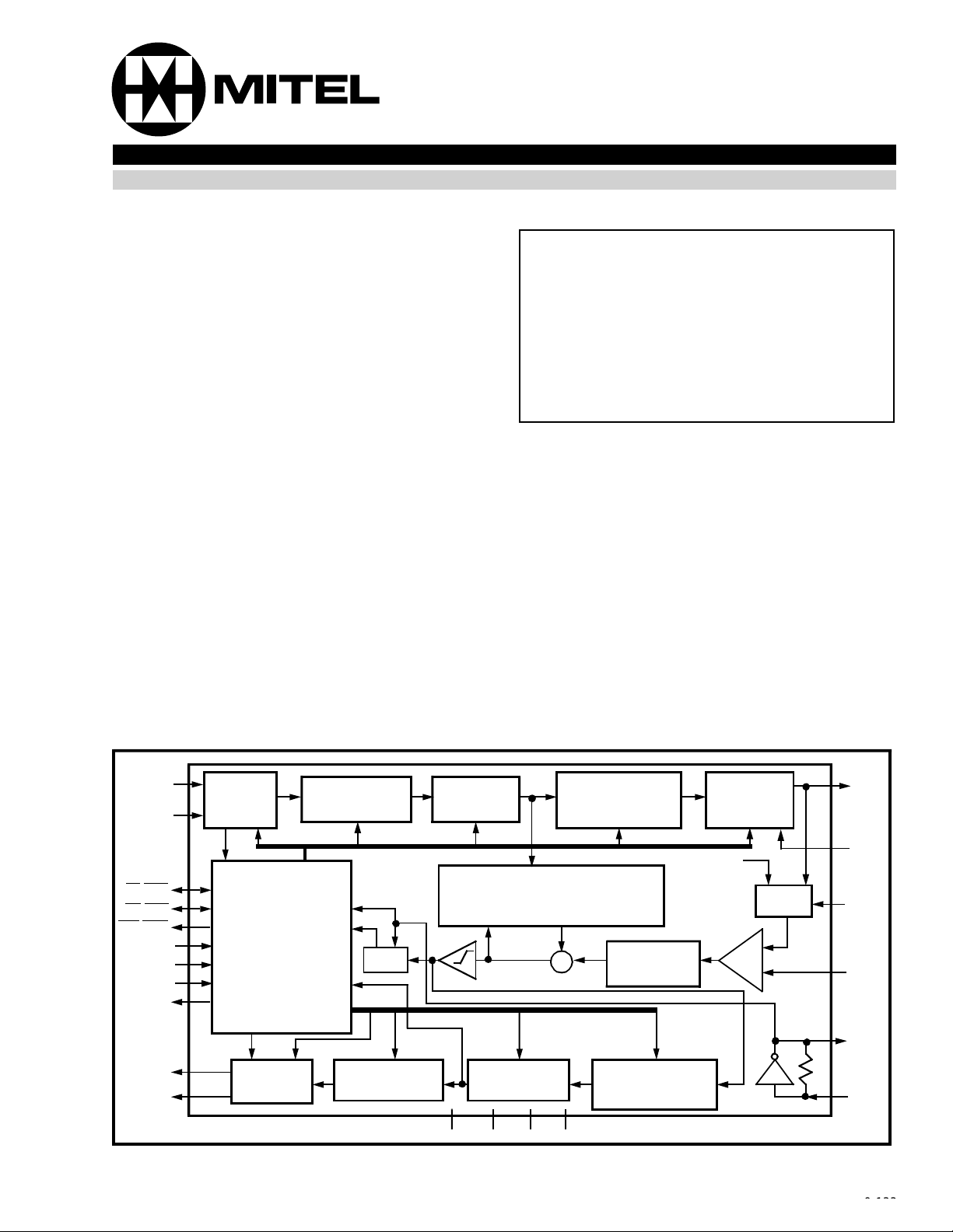
The MT9171 (DSIC) and MT9172 (DNIC) are multifunction devices capable of providing high speed,
full duplex digital transmission up to 160 kbit/s over
DSTi/Di
CDSTi/
CDi
/CLD
F0
C4/TCK
F0o/RCK
MS0
MS1
MS2
RegC
DSTo/Do
CDSTo/
CDo
Transmit
Interface
Control
Register
Transmit/
Clock
Receive
Timing &
Control
Status
Receive
Interfac e
Prescrambler Scrambler
Transmit
Timi ng
Master Clock
Phase Locked
Sync Detec t
Receive
DPLL
De-
Prescrambler
Error
Signal
V
DDVSSVBiasVRef
Figure 1 - Functional Block Diagram
Address
Echo Canceller
Echo Estimate
Descrambler
Differentially
Encoded Biphase
Transmitter
—
+
∑
Differenti all y
Encoded Biphase
Receive
Filter
Receiver
Transmit
Filter &
Line Driver
V
Bias
-1
+2
MUX
L
OUT
L
OUT
DIS
Precan
L
IN
OSC2
OSC1
9-1339-133
Page 2
MT9171/72 Advance Information
LOUT
VBias
VRef
MS2
MS1
MS0
RegC
/CLD
F0
CDSTi/CDi
CDSTo/CDo
VSS
1
2
3
4
5
6
7
8
9
10
11
22 PIN PDIP/CERDIP
22
21
20
19
18
17
16
15
14
13
12
VDD
LIN
TEST
LOUT DIS
Precan
OSC1
OSC2
/TCK
C4
F0o/RCK
DSTi/Di
DSTo/Do
LOUT
VBias
VRef
MS2
MS1
MS0
RegC
NC
/CLD
F0
CDSTi/CDi
CDSTo/CDo
VSS
1
2
3
4
5
6
7
8
9
10
11
12
24 PIN SSOP
24
23
22
21
20
19
18
17
16
15
14
13
MS2
MS1
MS0
RegC
F0
/CLD
VDD
LIN
TEST
LOUT DIS
Precan
OSC1
NC
OSC2
/TCK
C4
F0o/RCK
DSTi/Di
DSTo/Do
NC
NC
VBias
VRef
432
5
6
7
8
9
10
11
1213141516
CDSTi/CDi
CDSTo/CDo
28 PIN PLCC
LOUT
•
VSS
NC
1
DSTo/Do
VDD
28
17
DSTi/Di
LIN
27
/RCK
F0o
TEST
26
18
NC
25
24
23
22
21
20
19
NC
LOUT DIS
Precan
OSC1
OSC2
NC
/TCK
C4
Figure 2 - Pin Connections
Pin Description
Pin #
22 24 28
11 2 L
22 3 V
33 4 V
4,5,64,5,65,7,8MS2-MS0 Mode Select inputs (Digital). The logic levels present on these pins select the
77 9 RegCRegulator Control output (Digital). A 512 kHz clock used for switch mode power
89 10F0
9 10 12 CDS Ti/
10 11 13 CDSTo/
Name Description
OUT
Bias
Ref
Line Out. Transmit Signal output (Analog). Referenced to V
Internal Bias Voltage output. Connect via 0.33 µF decoupling capacitor to VDD.
Internal Reference V oltage output. Connect via 0.33 µF decoupling capacitor to
V
.
DD
Bias
.
various operating modes for a particular appl icati on. See Table 1 for the
operating modes.
supplies. Unused in MAS/MOD mode and should be left open circuit.
/CLD Frame Pulse/C-Channel Load (Digital). In DN mode a 244 ns wide negative
pulse input for the MASTER indicating the start of the active channel times of the
device. Output for the SLAVE indicating the start of the active channel times of
the device. Output in MOD mode providing a pulse indicating the sta rt of the Cchannel.
Control/Data ST-BUS In/Control/Data In (Digital). A 2.048 Mbit/ s serial cont rol
CDi
& signalling input in DN mode. In MOD m ode this is a contin uous bit strea m at
the bit rate selected.
Control/Data ST-BUS Out/Control/Data Out (Digi tal). A 2.048 Mbit/s serial
CDo
control & signalling out put in DN mo de. In MO D mode this is a conti nuous bit
stream at the bit rate selected.
9-134
Page 3
Advance Information MT9171/72
Pin Description (continued)
Pin #
Name Description
22 24 28
11 12 14 V
Negative Power Suppl y (0V ).
SS
12 13 15 DSTo/Do Data ST-BUS Out/Data Out (Digital). A 2.048 Mbit/s serial PCM/da ta out put in
DN mode. In MOD mode this is a continuous bit stream at the bit rate selected.
13 14 16 DS Ti/Di Data ST-BUS In/Data In (D i git al). A 2.048 Mbit /s serial PCM/ dat a input in DN
mode. In MOD mode this is a continuous bit stream at the bit rate selected.
14 15 17 F0o
/RCK Frame Pulse Out/Receive Bit Rate Clock output (Digital). In DN mode a 244 ns
wide negative pulse indicating the end of the active channel times of the device
to allow daisy chaining. In MOD mode provides the rece ive bit rate clock to the
system.
15 16 19 C4
/TCK Data Clock/Transmit Baud Rate Clock (Digital). A 4.096 M Hz TTL compatible
clock input for the MASTER and out put for the SLAVE in DN mode. For MOD
mode this pin provides the transmit bit rate clock to the system.
16 17 21 OSC2 Oscillator Output. CMOS Out put.
17 19 22 OSC1 Oscillator Input. CMOS Input. D.C. couple signals to this pin. Refer to D.C.
Electrical Characteristics for OSC1 input requirements.
18 20 23 Precan Precanceller Di sabl e. When held to Logic ’1
precanceller is forced to V
logic ’0’, the L
to the precanceller path is enabled and functions normally . An
OUT
thus bypassing the precanceller section. Wh en
Bias
’, the internal path from L
OUT
to the
internal pulldown (50 kΩ) is provided on this pin.
8,181,6,
NC No Connecti on . Leave ope n circuit
11,
18,
20,
25
19 21 24 L
OUT
DIS L
Disable. When held to logic “1”, L
OUT
logic “0”, L
functions normally. An internal pulldown (50 kΩ) is provided on this
OUT
is disabled (i.e., output = V
OUT
). When
Bias
pin.
20 22 26 TEST Test Pin. Connect to V
21 23 27 L
22 24 28 V
DD
Receive Signal input (A nalog ).
IN
Positi ve P ower Supply (+5V) input .
SS
.
9-135
Page 4
MT9171/72 Advance Information
AAAA
AAAA
AAAA
AAAA
AAAA
AAAA
AAAA
AAAA
AAAA
AAAA
AAAA
AAAA
AAAA
AAAA
AAAA
AAAA
AAAA
AAAA
AAAA
AAAA
AAAA
AAAA
AAAA
AAAA
AAAA
AAAA
AAAA
AAAA
AAAA
AAAA
AAAA
AAAA
AAAA
AAAA
AAAA
AAAA
AAAA
AAAA
AAAA
AAAA
AAAA
AAAA
AAAA
AAAA
AAAA
AAAA
AAAA
AAAA
AAAA
AAAA
AAAA
AAAA
AAAA
AAAA
AAAA
AAAA
AAAA
AAAA
AAAA
AAAA
AAAA
AAAA
AAAA
AAAA
AAAA
AAAA
AAAA
AAAA
AAAA
AAAA
AAAA
AAAA
AAAA
AAAA
AAAA
AAAA
AAAA
AAAA
AAAA
AAAA
AAAA
AAAA
AAAA
AAAA
AAAA
AAAA
AAAA
AAAA
AAAA
AAAA
AAAA
AAAA
AAAA
AAAA
AAAA
AAAA
AAAA
AAAA
AAAA
AAAA
AAAA
AAAA
AAAA
AAAA
AAAA
AAAA
AAAA
AAAA
AAAA
AAAA
AAAA
A
A
A
A
A
A
AAAA
A
A
A
A
A
A
A
AA
A
A
A
A
A
A
AAAA
AAAA
AAAA
AAAA
AAAA
AAAA
AAAA
AAAA
AAAA
AAAA
AA
AA
AA
AA
AA
AAAA
AAAA
AAAA
AAAA
AAAA
AAAA
AAAA
AAAA
AAAA
AAAA
AA
AA
AA
AA
AA
AAAA
AAAA
AAAA
AAAA
AAAA
AAA
AAA
AAA
AAA
AAA
AAAA
AAAA
AAAA
AAAA
AAAA
A
A
A
A
A
AAAA
AAAA
AAAA
AAAA
AAAA
AAA
AAA
AAA
AAA
AAA
AAAA
AAAA
AAAA
AAAA
AAAA
A
A
A
A
A
A
A
A
A
A
AA
A
A
A
A
AA
F0
C4
AAA
AAA
DSTi
DSTo
F0o
AAA
AAA
AAA
AAAA
AAAA
AAAA
AAAA
AAAA
B1
B1
B1
7
B1
7
B1
6
B1
6
B1
5
B1
5
B1
4
B1
4
B1
3
B1
3
B1
2
B1
2
B1
1
1
B1
0
0
B1
B1
7
7
Channel Time 0
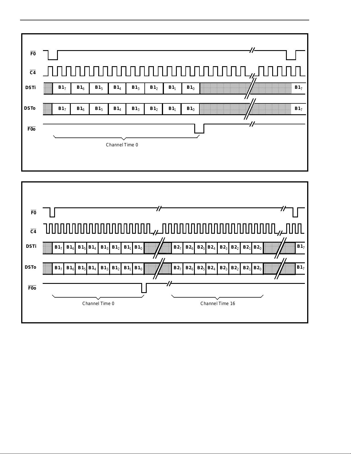
Figure 3 - DV Port - 80 kbit/s (Modes 2, 3, 6)
F0
C4
DSTi
DSTo
F0o
AAA
A
AAA
A
AAA
A
B17B16B15B14B13B12B11B1
AAA
A
AAA
A
AAA
A
AAA
A
B1
AAA
A
7B16B15B14B13B12B11B10
AAA
A
Channel Time 0
Figure 4 - DV Port - 160 kbit/s (Modes 2, 3, 6)
0
B27B26B25B24B23B22B21B2
B27B26B25B24B23B22B21B2
0
0
B1
B1
7
7
Channel Time 16
9-136
Page 5

Advance Information MT9171/72
L
Functional Description
The MT9171/72 is a device which has been
designed primarily as an interface for the Integrated
Services Digital Network (ISDN). However, it may be
used in practically any application that requires high
speed data transmission over two wires, including
smart telephone sets, workstations, data terminals
and com p uters.
). The data on the line is made up of information
OUT
from the DV and CD ports. The DNIC must combine
information received from both the DV and CD ports
and put it onto the line. At the same time, the data
received from the line must be split into the various
channels and directed to the proper ports. The
usable data rates are 72 and
144 kbit/s as required
for the basic rate interface in ISDN. Full duplex
transmission is made possible through on board
adaptive echo cancellation.
In the ISDN, the DNIC is ideal for providing the
interface at the U reference point. The device
supports the 2B+D channel format (two 64 kbit/s Bchannels and one 16 kbit/s D-channel) over two
wires as recommended by the CCITT. The line data
is converted to and from the ST-BUS format on the
system side of the network to allow for easy
interfacing with other components such as the Sinterface device in an NT1 arrangement, or to digital
PABX components.
Smart telephone sets with data and voice capability
can be easily implemented using the MT9171/72 as
a line interface. The device’s high bandwidth and
long loop length capability allows its use in a wide
variety of sets. This can be extended to provide full
data and voice capability to the private subscriber by
the installation of equipment in both the home and
central office or remote concentration equipment.
Within the subscriber equipment the MT9171/72
would terminate the line and encode/ decode the
data and voice for transmission while additional
electronics could provide interfaces for a standard
telephone set and any number of data ports
supporting standard data rates for such things as
computer communications and telemetry for remote
meter reading. Digital workstations with a high
degree of networking capability can be designed
using the DNIC for the line interface, offering up to
160 kbit/s data transmission over existing telephone
lines. The MT9171/72 could also be valuable within
existing computer networks for connecting a large
number of terminals to a computer or for
intercomputer links. The highest data rates existing
for terminal to computer links is 19.2 kbit/s over
conventional analog modems. With the DNIC, this
can be increased up to 160 kbit/s at a very low cost
per line for terminal to computer links and in many
cases this bandwidth would be sufficient for
computer to computer links.
Figure 1 shows the block diagram of the MT9171/72.
The DNIC provides a bidirectional interface between
the DV (data/voice) port and a full duplex line
operating at 80 or 160 kbit/s over a single pair of
twisted wires. The DNIC has three serial ports. The
DV port (DSTi/Di, DSTo/Do), the CD (control/data)
port (CDSTi/CDi, CDSTo/CDo) and a line port (L
IN
The DNIC has various modes of operation which are
selected through the mode select pins MS0-2. The
two major modes of operation are the MODEM
(MOD) and DIGITAL NETWORK (DN) modes. MOD
mode is a transparent 80 or 160 kbit/s modem. In
DN mode the line carries the B and D channels
formatted for the ISDN at either 80 or 160 kbit/s. In
the DN mode the DV and CD ports are standard STBUS and in MOD mode they are transparent serial
data streams at 80 or 160 kbit/s. Other modes
include: MASTER (MAS) or SLAVE (SLV) mode,
where the timebase and frame synchronization are
provided externally or are extracted from the line and
DUAL or SINGLE (SINGL) port modes, where both
the DV and CD ports are active or where the CD port
is inactive and all information is passed through the
DV port. For a detailed descript ion of the modes
“Operating Modes” section.
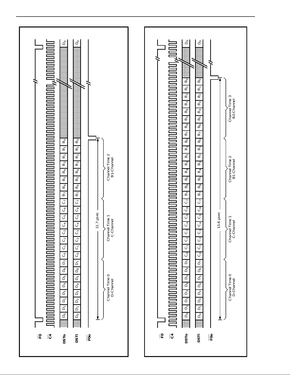
In DIGITAL NETWORK (DN) mode there are three
channels transferred by the DV and CD ports. They
are the B, C and D channels. The B1 and B2
channels each have a bandwidth of 64 kbit/s and are
used for carrying PCM encoded voice or data. These
channels are always transmitted and received
through the DV port (Figures 3, 4, 5, 6). The Cchannel, having a bandwidth of 64 kbit/s, provides a
means for th e s y s te m to co n tro l th e D N IC and for the
DNIC to pass status information back to the system.
The C-channel has a Housekeeping (HK) bit which is
the only bit of the C-channel transmitted and
received on the line. The 2B+D channel bits and the
HK bit are double-buffered. The D-channel can be
transmitted or received on the line with either an 8,
16 or 64 kbit/s bandwidth depending on the DNIC’s
mode of operation. Both the HK bit and the Dchannel can be used for end-to-end signalling or low
speed data transfer. In DUAL port mode the C and D
channels are accessed via the CD port (Figure 7)
while in SINGL port mode they are transferred
through the DV port (Figures 5, 6) along with the B1
and B2 channels.
,
see
9-137
Page 6
MT9171/72 Advance Information
A
A
A
A
A
A
A
A
A
A
A
A
A
A
A
A
A
A
A
A
A
A
A
A
A
A
A
A
A
A
A
A
A
A
A
A
A
A
A
A
A
A
A
A
A
A
A
A
A
A
A
A
A
A
A
A
A
A
A
A
A
A
A
A
A
A
A
A
A
A
A
A
A
A
A
A
A
A
A
A
A
A
A
A
A
A
A
A
A
A
A
A
A
A
A
A
A
A
A
A
A
A
A
A
A
A
A
A
A
A
A
A
A
A
A
A
A
A
A
A
A
A
A
A
A
AA
A
A
A
A
A
A
A
A
A
A
A
A
A
A
A
A
A
A
A
A
A
A
A
A
A
A
AA
AAA
AAA
AAA
AAA
AAA
AAA
AAA
AAA
AAA
AAA
AAA
AAA
AAA
AAA
AAA
AAA
AAA
AAA
AAA
AAA
0
0
D
D
AAA
A
AAA
A
AAA
A
AAA
A
AAA
A
AAA
A
AAA
A
AAA
A
AAA
A
AAA
A
AAA
A
AAA
A
AAA
A
AAA
A
AAA
A
AAA
A
0
0
B
B
1
1
B
B
2
2
B
B
3
3
B
B
4
4
B
B
5
5
B
B
6
6
B
B
7
7
B
B
0
0
B
B
1
1
B
B
2
2
B
B
3
3
B
B
4
4
B
B
5
5
B
B
6
6
B
B
7
7
B
B
7
7
C
C
6
6
C
C
5
5
C
C
4
4
C
C
3
3
C
C
2
2
C
C
1
1
C
C
0
0
C
C
7
7
D
D
6
6
D
D
5
5
D
D
4
4
D
D
3
3
D
D
2
2
D
D
1
1
D
D
0
0
D
D
AAA
A
AAA
A
AAA
A
AAA
A
DSTi
DSTo
15.6 µsec
F0o
B2-Channel
Channel Time 3
B1-Cha nnel
Channel Time 2
C-Channel
Figure 6 - DV Port - 16 0 k bit/s (Mo des 0 ,4)
Channe l Tim e 1
D-Channel
Channel Time 0
0
0
D
D
AAAA
AAAA
AAAA
AAAA
AAAA
AAAA
AAAA
AAAA
AAAA
AAAA
AAAA
AAAA
AAAA
AAAA
AAAA
AAAA
AAAA
AAAA
AAAA
AAAA
AAAA
AAAA
AAAA
AAAA
AAAA
AAAA
AAAA
AAAA
AAAA
AAAA
AAAA
AAAA
AAAA
AAAA
AAAA
AAAA
AAAA
AAAA
AAAA
AAAA
AAAA
AAAA
AAAA
AAAA
AAAA
AAAA
AAAA
AAAA
AAAA
AAAA
9-138
F0
C4
AAAA
AAAA
AAAA
AAAA
AAA
AAA
AAA
AAA
AAA
AAA
AAA
AAA
AAA
AAA
AAA
AAA
AAA
AAA
AAA
AAA
AAA
AAA
AAA
AAA
AAA
AAA
AAA
AAA
AAA
AAA
AAA
AAA
AAA
AAA
AAA
AAA
AAA
AAA
AAA
AAA
AAA
AAA
AAA
AAA
AAA
AAA
AAA
AAA
AAA
AAA
AAA
AAA
AAA
AAA
0
0
B
B
1
1
B
B
2
2
B
B
3
3
B
B
4
4
B
B
5
5
B
B
6
6
B
B
7
7
B
B
7
7
C
C
6
6
C
C
5
5
C
C
4
4
C
C
3
3
C
C
2
2
C
C
1
1
C
C
0
0
C
C
7
7
D
D
6
6
D
D
5
5
D
D
4
4
D
D
3
3
D
D
2
2
D
D
1
1
D
D
0
0
D
D
AAA
AAA
AAA
AAA
DSTi
DSTo
11.7 µsec
F0o
B1-Cha nnel
Channel Time 2
C-Channel
Figure 5 - DV Port - 80 kbit/s (Modes 0,4)
Channel Time 1
D-Channel
Channel Time 0
F0
C4
Page 7
Advance Information MT9171/72
AAAA
AAAA
AAAA
AAAA
AAAA
AAAA
AAAA
AAAA
AAAA
AAAA
AAAA
AAAA
AAAA
AAAA
AAAA
AAAA
AA
AAAA
AAAA
AAAA
AAAA
AAAA
AAAA
AAAA
AAAA
AAAA
AAAA
AAAA
AAAA
A
A
A
A
A
A
AAAA
AAAA
AAAA
AAAA
AAAA
AAAA
AAAA
AAAA
A
A
A
A
A
A
A
A
A
AAAA
AAAA
AAAA
AAAA
AAAA
AAAA
AAAA
AAAA
AAAA
AAAA
AAAA
AAAA
AA
AA
AA
AA
AA
AA
AAAA
AAAA
AAAA
A
AAAA
AAAA
AAAA
AAAA
AAAA
AAAA
AAAA
AAAA
AAAA
AAAA
AAAA
AAAA
AAAA
AAAA
AAAA
AAAA
AAAA
AAAA
AAAA
AAAA
AAAA
AAAA
AAAA
AAAA
AAAA
A
A
A
A
A
AAAA
AAAA
AAAA
AAAA
AAAA
AAAA
AAAA
AAAA
AAAA
AAAA
A
A
A
A
A
A
A
A
A
A
AAAA
AAAA
AAAA
AAAA
AAAA
AAAA
AAAA
AAAA
AAAA
AAAA
AA
AA
AA
AA
AA
AAAA
AAAA
AAAA
AAAA
AAAA
AAAA
AAAA
AAAA
AAAA
AAAA
AAAA
AAA
AAAA
AAAA
AAAA
AAAA
AAAA
AAAA
AAAA
AAAA
AAAA
AAAA
AAAA
AAAA
AAAA
AAAA
AAAA
AAAA
AAA
AAA
AAA
AAA
AAAA
AAAA
AAAA
AAAA
AAAA
AAAA
AAAA
AAAA
AAAA
AAAA
AAAA
AAAA
AAA
AAA
AAA
AAA
AAA
AAA
AAAA
AAAA
AAA
AAAA
AAAA
AAAA
AAAA
AAAA
AAAA
AAAA
AAAA
AAAA
AAAA
AAAA
AAAA
AAAA
AAAA
AAAA
AAAA
AAAA
AAAA
AAAA
AAAA
AAAA
AAAA
AAAA
AAAA
AAAA
AAA
AAA
AAA
AAA
AAA
AAAA
AAAA
AAAA
AAAA
AAAA
AAAA
AAAA
AAAA
AAAA
AAAA
AAA
AAA
AAA
AAA
AAA
A
A
A
A
A
A
A
A
A
A
A
AA
A
In DIGITAL NETWORK (DN) mode, upon entering
the DNIC from the DV and CD ports, the B-channel
data, D-channel D0 (and D1 for 160 kbit/s), the HK
bit of the C-channel (160kbit/s only) and a SYNC bit
are combined in a serial format to be sent out on the
line by the Transmit Interface (Figures 11, 12). The
SYNC bit produces an alternating 1-0 pattern each
frame in order for the remote end to extract the frame
alignment from the line. It is possible for the remote
end to lock on to a data bit pattern which simulates
this alternating 1-0 pattern that is not the true SYNC.
To decrease the probability of this happening the
DNIC may be programmed to put the data through a
prescrambler that scrambles the data according to a
predetermined polynomial with respect to the SYNC
bit. This greatly decreases the probability that the
SYNC pattern can be reproduced by any data on the
line. In order for the echo canceller to function
correctly, a dedicated scrambler is used with a
scrambling algorithm which is different for the SLV
and MAS modes. These algorithms are calculated in
such a way as to provide orthogonality between the
F0
near and far end data streams such that the
correlation between the two signals is very low.
For any two DNICs on a link, one must be in SLV
mode with the other in MAS mode. The scrambled
data is differentially encoded which serves to make
the data on the line polarity-independent. It is then
biphase encoded as shown in Figure 10. See “Line
Interface” section for more details on the encoding.
Before leaving the DNIC the differentially encoded
biphase data is passed through a pulse-shaping
bandpass transmit filter that filters out the high and
low frequency components and conditions the signal
for transmission on the line.
The composite transmit and receive signal is
received at L
. On entering the DNIC this signal
IN
passes through a Precanceller which is a summing
amplifier and lowpass filter that partially cancels the
near-end signal and provides first order antialiasing
for the rec eive d signa l. Inte rnal , part ial c ancell atio n
C4
CDSTo
CDSTi
F0o
CLD
TCK
AAA
AAA
C0C1C2C3C4C5C6C
AAA
AAA
AAA
AAA
C0C1C2C3C4C5C6C
AAA
AAA
AAA
3.9 µsec
Channel Time 0 Channel Time 16
62.5 µsec
7
7
D0D1D2D3D4D5D6D
D0D1D2D3D4D5D6D
125 µsec
Figure 7 - CD Port (Modes 2,6)
7
7
C
0
C
0
CDi
CDo
C
6
C
6
C
7
C
7
C
0
C
0
C
1
C
1
C
2
C
2
C
3
C
3
C
4
C
4
C
5
C
5
C
6
C
6
C
7
C
7
C
0
C
0
C
1
C
1
Figure 8 - CD Port (Modes 1,5)
9-139
Page 8

MT9171/72 Advance Information
of the near end signal may be disabled by holding
the Precan pin high. This mode simplifies the design
of external line transceivers used for loop extension
applications. The Precan pin features an internal
pull-down which allows this pin to be left
unconnected in applications where this function is
not required. The resultant signal passes through
a receive filter to bandlimit and equalize it. At this
point, the echo estimate from the echo canceller is
subtracted from the precancelled received signal.
This difference signal is then input to the echo
canceller as an error signal and also squared up by a
comparator and passed to the biphase receiver.
Within the echo canceller, the sign of this error signal
is determined. Depending on the sign, the echo
estimate is either incremented or decremented and
this new es tim a te is stored ba c k i n R AM.
The timebase in both SLV and MAS modes
(generated internally in SLV mode and externally in
MAS mode) is phase-locked to the received data
stream. This phase-locked clock operates the
Biphase Decoder, Descrambler and Deprescrambler
in MAS mode and the entire chip in SLV mode. The
Biphase Decoder decodes the received encoded bit
stream resulting in the original NRZ data which is
passed onto the Descrambler and Deprescrambler
where the data is restored to its original content by
performing the reverse polynomials. The SYNC bits
are extracted and the Receive Interface separates
the channels and outputs them to the proper ports in
the proper channel times. The destination of the
various channels is the same as that received on the
input DV and CD ports.
The Transmit/Receive Timing and Control block
generates all the clocks for the transmit and receive
functions and controls the entire chip according to
the control register. In order that more than one
DNIC may be connected to the same DV and
CD ports an F0o
the next device in a daisy chain that its channel
times are now active. In this arrangement only
signal is generated which signals
the first DNIC in the chain receives the system F0
with the following devices receiving its predecessor’s
F0o
.
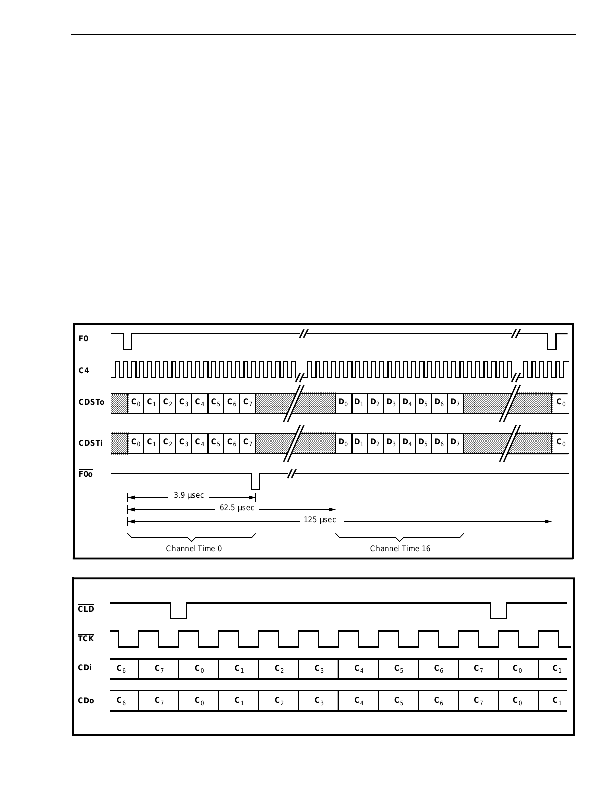
In MOD mode, all the ports have a different format.
The line port again operates at 80 or 160 kbit/s,
however, there is no synchronization overhead, only
transparent data. The DV and CD ports carry serial
data at 80 or 160 kbit/s with the DV port transferring
all the data for the line and the CD port carrying the
C-channel only. In this mode the transfer of data at
both ports is synchronized to the TCK
clocks for transmit and receive data, respectively.
The CLD
C-channel data on the CD port. It is used to load and
latch the input and output C-channel but has no
relationship to the data on the DV port.
Operating Modes (MS0-2)
The logic levels
MS0, MS1 and MS2 program the DNIC for different
operating modes and configure the DV and CD ports
accordingly. Table 1 shows the modes
corresponding to the state of MS0-2. These pins
select the DNIC to operate as a MASTER or SLAVE,
in DUAL or SINGLE port operation, in MODEM or
DIGITAL NETWORK mode and the order of the C
and D channels on the CD port. Table 2 provides a
description of each mode and Table 3 gives a pin
configuration according to the mode selected for all
pins that have variable functions. These functions
vary depending on whether it is in MAS or SLV, and
whether DN or MOD mode is used.
The overall mode of operation of the DNIC can be
programmed to be either a baseband modem
(MOD mode) or a digital network transceiver (DN
mode). As a baseband modem, transmit/receive
data is passed transparen tly thr ough the device at 80
signal goes low to indicate the start of the
present on the mode select pins
and RCK
Mode Selec t Pins
MS2 MS1 MS0 SLV MAS DUAL SINGL MOD DN D-C C-D ODE
00 0 0 E E E E E
001 1 E E E XXE
01 0 2 E E E E E
01 1 3 E E E E E
10 0 4 E E E E E
101 5E E E XXE
11 0 6 E E E E E
11 1 7 E E E E
E=Enabled X=Not Applicable
Blanks are disabled
9-140
Mode
Ta ble 1. Mode Select Pins
Operating Mod e
Page 9

Advance Information MT9171/72
or 160 kbit/s by the DV port. The CD port transfers
the C-channel and D-Channel also at 80 or 160
kbit/s.
In DN mode, both the DV and CD ports operate as
ST-BUS streams at 2.048 Mbit/s. The DV port
transfers data over pins DSTi and DSTo while on the
CD port, the CDSTi and CDSTo pins are used. The
SINGL port option only exists in DN mode.
In MOD mode, DUAL port operation must be used
and the D, B1 and B2 channel designations no
longer exist. The selection of SLV or MAS will
determine which of the DNICs is using the externally
Mode Function
- The chip timebase is extracted from the received line data and the ext ernal 10. 24 MHz
- The timebase is derived from the externall y supplied data clocks and 10.24 MHz clock
- Both the CD and DV ports are active with the CD port transferring the C&D channels
- Baseband operation at 80 or 160 kbits/s. The line data is received and transmitted
- Intended for use in the digital network with the DV and CD ports operating at
SLV
MAS
DUAL
SIN GL
MOD
DN
SLAVE
crystal is phase locked to it to provide clocks for the entire device and are output for the external
system to synchronize to.
MASTER
which must be frequency locked. Th e transmit data is synchronized to the system timing with the
receive data recovered by a clock extracted from the receive data and resynchronized to the system
timing.
DUAL PORT
and the DV port transferring the B1& B2 channels.
SINGLE PORT - The B1& B2, C and D channels are all transferred through the DV port. The CD
port is disabled and CDSTi should be pulled high.
MODEM
through the DV port at the baud rate selected. The C-channel is transferred through the CD port
also at the baud rate and is synchronized to t he CLD
DIGITAL NETWORK
2.048 Mbits/s and the lin e at 80 or 160 kbits/s configured according to the applica ble ISDN
recommendation.
supplied clock and which is phase locking to the data
on the line. Due to jitter and end to end delay, one
end must be the master to generate all the timing for
the link and the other must extract the timing from
the receive data and synchronize itself to this timing
in order to recover the synchronous data. DUAL port
mode allows the user to use two separate serial
busses: the DV port for PCM/data (B channels) and
the CD port for control and signalling information (C
and D channels). In the SINGL port mode, all four
channels are concatenated into one serial stream
and input to the DNIC via the DV port. The order of
the C and D channels may be changed only in DN/
DUAL mode. The DNIC may be configured to
output.
D-C D BEFORE C-CHANNEL
C-D C BEFORE D-CHANNEL
OUTPUT DATA ENABLE
ODE
Mode
#
0F0
1CLD
2F0
3F0
4F0
5CLD
6F0
7F0
impedance state. This is intended for power-up reset to avoid bus contention and possible damage
to the device during the initial random state in a daisy chain configu ra tio n of DNICs. In all the other
modes of operation DV and CD ports are enabled during the appropriate channel times.
F0
/CLD F0o/RCK C4/TCK
Name Input/Outp ut Name Inp ut/ Outp ut Name Input/O utp ut
Output RCK Output TCK Outp ut
Output F0o Outp ut C4 Output
Output RCK Output TCK Outp ut
Output F0o Outp ut C4 Output
- The D-channel is transferred before the C-channel following F0.
- The C-channel is transferred before the D-channel following F0.
- When mode 7 is selected, the DV and CD ports are put in high
Table 2. Mode Definitions
Input F0o Output C4 Input
Input F0o Output C4 Input
Input F0o Output C4 Input
Input F0o Output C4 Input
Ta ble 3. Pin Configurations
9-141
Page 10

MT9171/72 Advance Information
transfer the D-channel in channel 0 and the Cchannel in channel 16 or vice versa. One other
feature exists; ODE, where both the DV and CD
ports are tristated in order that no devices are
damaged due to excessive loading while all DNICs
are in a random state on power up in a daisy chain
arrangement.
DV Port (DSTi/Di, DSTo/Do)
The DV port transfers data or PCM encoded voice to
and from the line according to the particular mode
selected by the mode select pins. The modes
affecting the configuration of the DV port are MOD or
DN and DUAL or SINGL. In DN mode the DV port
operates as an ST-BUS at 2.048 Mbit/s with 32, 8 bit
channels per frame as shown in Figure 9. In this
mode the DV port channel configuration depends
upon whether DUAL or SINGL port is selected.
When DUAL port mode is used, the C and D
channels are passed through the CD port and the B1
and B2 channels are passed through the DV port. At
80 kbit/s only one channel of the available 32 at the
DV port is utilized, this being channel 0 which carries
the B1-channel. This is shown in
kbit/s, two channels are used, these
Figure 3. At 160
being 0 and 16
carrying the B1 and B2 channels, respectively. This
is shown in Figure 4. When SINGL port mode is
used, channels B1, B2, C and D are all passed via
the DV port and the CD port is disabled. See CD port
description for an explanation of the C and D
channels.
The D-channel is always passed during channel t ime
0 followed by the C and B1 channels in channel
times 1 and 2, respectively for 80 kbit/s. See Figure
5. For 160 kbit/s the B2 channel is added and
occupies channel time 3 of the DV port. See Figure
6. For all of the various configurations the bit orders
are shown by the respective diagram. In MOD mode
the DV and CD ports no longer operate at 2.048
Mbits/s but are continuous serial bit streams
operating at the bit rate selected of 80 or 160 kbit/s.
While in the MOD mode only DUAL port operation
can be used.
In order for more than one DNIC to be connected to
any one DV and CD port, making more efficient use
of the busses, the DSTo and CDSTo outputs are put
into high impedance during the inactive channel
times of the DNIC. This allows additional DNICs to
be cascaded onto the same DV and CD ports. When
used in this way a signal called F0o
is used as an
indication to the next DNIC in a daisy chain that its
channel tim e is n o w ac tive . O nly th e fi rs t D NI C in the
chain receives the system frame pulse and all
others receive the F0o
from its predecessor in
the chain. This allows up to 16 DNICs to be
cascaded.
CD Port (CDSTi/CDi, CDSTo/CDo)
The CD port is a serial bidirectional port used only in
DUAL port mode. It is a means by which the DNIC
receives its control information for things such as
setting the bit rate, enabling internal loopback tests,
sending status information back to the system and
transferring low speed signalling data to and from
the line.
The CD port is composed of the C and D-Channels.
The C-channel is used for transferring control and
status information between the DNIC and the
system. The D-channel is used for sending and
receiving signalling information and lower speed
data between the line and the system. In DN/DUAL
mode the DNIC receives a C-channel on CDSTi
while transmitting a C-channel on
CDSTo. Fifteen
channel times later (halfway through the frame) a Dchannel is received on CDSTi while a D-channel is
transmitted on CDSTo. This is shown in Figure 7.
The order of the C and D bytes in DUAL port mode
can be reversed by the mode select pins. See Table
1 for a listing of the byte orientations.
The D-channel exists only in DN mode and may be
used for transferring low speed data or signalling
ST-BUS
9-142
F0
Chan nel
31
Channel0Channel1Channel
Significant
Bit (First)
Most
2
Bit 7 Bit 6 Bit 5 Bit 4 Bit 3 Bit 2 Bit 1 Bit 0
Figure 9 - ST-BUS Format
125 µsec
• • • • • • • •
Channel
3.9 µsec
29
Channel30Channel31Channel
0
Least
Significant
Bit (Last)
Page 11

Advance Information MT9171/72
information over the line at 8, 16 or 64 kbit/s (by
using the DINB feature). The information passes
transparently through the DNIC and is transmitted to
or received from the line at the bit rate selected in
the Control Register.
If the bit rate is 8 0 kbit/s, o nly D0 is tran smitted a nd
received. At 160 kbit/s, D0 and D1 are transmitted
and receiv ed . W h e n th e DI NB bit i s set i n th e C o nt rol
Register the entire D-channel is transmitted and
received in the B1-channel timeslot.
The C-channel is used for transferring control and
status information between the DNIC and the
system. The Control and Diagnostics Registers are
accessed through the C-channel. They contain
information to control the
DNIC and carry out the
diagnostics as well as the HK bit to be transmitted on
the line as described in Tables 4 and 5. Bits 0 and 1
of the C-channel select between the Control and
bit 0 bit 1 bit 2 bit 3 bit 4 bit 5 bit 6 bit 7
Diagnostics Register. If these bits are 0, 0 then the
C-channel information is written to the Control
Register (Table 4). If they are 0, 1 the C-
channel is
written to the Diagnostics Register (Table 5).
The Diagnostics Register Reset bit (bit 2) of the
Control Register determines the reset state of the
Diagnostics Register. If, on writing to the Control
Register, this bit is set to logic “0”, the Diagnostics
Register will be reset coincident with the frame
pulse. When this bit is logic “1”, the Diagnostics
Register will not be reset. In order to use the
diagnostic features, the Diagnostics Register must
be continuously written to. The output C-channel
sends status information from the Status Register to
the system along with the received HK bit as shown
in Table 6.
In MOD m ode, the CD port is no longe r an ST-BUS
but is a serial bit stream operating at the bit rate
Reg Sel-1 Reg Sel-2 DRR BRS DINB PSEN ATTACK TxHK
Default Mode Selection (Refer to Table 4a)
Bit Name Description
0 Reg Sel-1 Register Select-1. Must be set to ’0’ to select the Control Registe r.
1 Reg Sel-2 Register Select-2. Must be set to ’0’ to select the Control Registe r.
2 DRR Diagnostics Register Reset. Writing a "0" to this bit will cause a diagnostics register reset
to occur coincident with the next frame pulse as in the MT8972A. When this bit is a logic
"1", the Diagnostics Register will not be reset.
3 B RS Bit Rate Select. When set to ’0’ selects 80 kbit/s. When set to ’1’, selects 160 kbit/s.
4DINB
➁
D-Channel in B Timeslot. When ’0’, the D-channel bits (D0 or D0 and D1) corresponding
to the selected bit rate (80 or 160 kbit/s) are transmitted during the normal D-cha nnel bit
times. When set to ’1’, the entire D-channel (D0-D7) is transmitted during the B1-channel
timeslot on the line providing a 64 kbit/s D-channel link.
5 PSEN
➁
Prescrambler/Deprescrambler Enable. When set to ’1’, the data prescrambler and
deprescrambler are enabled. When set to ’0’, the data prescrambler and deprescrambler
are disabled.
➁
6ATTACK
Convergence Speedup. When set to ’1’, the echo canceller will converge to the reflection
coefficient much faster. Used on power-up for fast convergence.
➀
When ’0’, the echo
canceller will require the normal amount of time to converge to a reflection coefficient.
7 TxHK
➁
Transmit Housekeeping. When set to ’0’, logic zero is transmitted over the line as
Housekeeping B it. When set to ’1’, logic one is transmitt ed over the line as
Housekeeping B it.
Table 4. Control Register
Notes:
➀ Suggested use of ATTACK:
-At 160 k b it/s f ul l c on v er g en ce re qu ir e s 85 0 ms with ATTACK he ld h igh fo r t he fi r st 24 0 fra me s or 30 m s.
-At 80 kb it /s fu ll conve rge nc e r eq ui res 1 .75 s with ATTA CK he ld h igh fo r t he fi r st 48 0 frames or 60 m s.
➁ When bits 4-7 o f the Control Reg is te r a re a ll s et to one, the DNIC o pe rates in o ne o f th e default m od es a s de fined in Table 4a,
dependin g up on th e s tatus of bit-3.
9-143
Page 12

MT9171/72 Advance Information
C-Channel
(Bit 0-7)
XXX01111 00000000 01000000 Default Mode-1
Internal Control
Regis ter
Internal Diagnosti c
Register
Description
➂
: Bit rate is 80 kbit/s. ATTACK ,
PSEN, DINB, DRR and all diagnostics are disabled.
TxHK=0.
XXX11111 00010000 01000000 Default Mode-2
➃
Bit rate is 160 kbit/ s. ATTA CK,
PSEN, DINB, DRR and all diagnostics are disabled.
TxHK=0.
Table 4a. Default Mode Selection
Notes:
➂ Default Mod e 1 ca n als o be s elected by ty in g CDSTi/CD i p in lo w w h en DN IC is operating i n d ua l mode.
➃ Defaul t M od e 2 can als o be s elected by ty in g CDSTi/CD i p in h igh when DN IC is operating i n d ua l mode.
bit 0 bit 1 bit 2 bit 3 bit 4 bit 5 bit 6 bit 7
Reg Sel-1 Reg Sel-2 Loopback FUN PSWAP DLO Not Used
Default Mode Selection
(Refer to Table 4a)
Bit Nam e Description
0 Reg Sel-1 Register Select-1. Must be set to ’0’ to select the Diagnostic Register.
1 Reg Sel-2 Register Select-2. Must be set to ’1’ to select the Diagnostic Register.
2,3 Loopback Bit 2
Bit 3
0 0 All loopback testing fun ction s disabled. Normal operation .
4FUN
➀
0 1 DSTi internally looped back into DSTo for system diagnostics.
10L
is internally looped back into LIN for system diagnostics.
OUT
1 1 DSTo is internally looped back into DSTi for end-to-end testing.
Force Unsync. When set to ’1’, the DNIC is forced out-of- s ync to test the SYNC
➁
➂
recovery circuitry. When set to ’0’, the operation continues in synchronization.
5 PSWAP
➀
Polynomial Swap. When set to ’1’, the scrambli ng and descrambling polynom ia ls
are interchanged (use for MAS mode only). When set to ’0’, the polynomials retain
their normal designations.
6DLO
➀
Disable Line Out. When set to ’1’, the signal on L
’0’, L
pin functions normall y.
OUT
is set set to V
OUT
. When set to
Bias
7 Not Used Must be set to ’0’ for normal operation.
Table 5. Diagnostic Register
Notes:
➀ When bits 4-7 of the Diagnostic Register are all set to o ne, the DNIC operates in one o f the default modes as defined in Table 4a,
depend in g up on th e s t a tu s of bi t- 3.
➁ Do not use L
to LIN loopback i n DN/ SLV mode.
OUT
➂ Do not u se D STo to DSTi loopb ack in M O D/M AS m o de .
, L
selected. It continues to transfer the C-channel but
Line Port (L
IN
OUT
)
the D-channel and the HK bit no longer exist. DUAL
port operation must be used in MOD mode. The Cchannel is clocked in and out of the CD port by TCK
and CLD with TCK defining the bits and CLD the
channel boundaries of the data stream as shown in
Figure 8.
The line interface is made up of L
L
driving the transmit signal onto the line and L
OUT
and LIN with
OUT
receiving the composite transmit and receive signal
from the line. The line code used in the DNIC is
Biphase and is shown in Figure 10. The scrambled
NRZ data is differentially encoded meaning the
previous differential encoded output is XOR’d with
the current data bit which produces the current
output. This is then biphase encoded where
IN
9-144
Page 13

Advance Information MT9171/72
01234567
SYNC CHQual Rx HK Future Functionality ID
Status
Register
Name Functio n
0 SYNC Synchronization - When set this bit indicates that synchronization to the received
line data sync patt ern has been acqui red. For DN mode only.
1-2 CHQual Channel Quality - These bits provide an estimat e of the receiver’s margin against
noise. The farther this 2 bit value is from 0 the better the SNR.
3 Rx
HK Housekeeping - This bit is the received housekeeping (HK) bit from the far end.
4-6 Future Fu ture Fu ncti on al ity. These bits return Logic 1 when read.
7 ID This bit provides a hardware identifier for the DNIC revision. The MT9171/72 will
return a logic “0” for this bit. (Logic “1” returned for MT8972A.)
Table 6. Status Registe r
transitions occur midway through the bit cell with a
negative going transition indicating a logic "0" and a
positive going transition indicating a logic "1".
The frame format of the transmit data on the line is
shown in Figures 11 and 12 for the DN mode at 80
and 160 kbit/s. At 80 kbit/s a SYNC bit for frame
recovery, one bit of the D-channel and the B1-
There are some major reasons for using a biphase
line code. The power density is concentrated in a
spectral region that minimizes dispersion and
channel are transmitted. At 160 kbit/s a SYNC bit,
the HK bit, two bits of the D-channel and both B1 and
B2 channels are transmitted.
differential attenuation. This can shorten the line
response and reduce the intersymbol interference
which are critical for adaptive echo cancellation.
There are regular zero crossings halfway through
every bit cell or baud which allows simple clock
extraction at the receiving end. There is no D.C.
content in the code so that phantom power feed may
be applied to the line and simple transformer
If the DINB bit of the Control Register is set, the
entire D-channel is transmitted during the B1-
channel timeslot. In MOD mode the SYNC, HK and
D-channel bits are not transmitted or received but
rather a continuous data stream at 80 or 160 kbit/s is
present. No frame recovery information is present on
the line in MOD mode.
coupling may be used with no effect on the data. It is
bipolar, making data reception simple and providing
a high signal to noise ratio. The signal is then passed
through a bandpass filter which conditions the signal
for the line by limiting the spectral content from
0.2f
Baud
to 1.6f
and on to a line driver where it is
Baud
made available to be put onto the line biased at
. The resulting transmit signal will have a
V
Bias
distributed spectrum with a peak at 3/4f
transmit signal (L
L
DIS pin high or by writing DLO (bit 6) of the
OUT
) may be disabled by holding the
OUT
Baud
. The
Diagnostics Register to logic “1”. When disabled,
is forced to the V
L
OUT
level. L
Bias
DIS has an
OUT
internal pull-down to allow this pin to be left not
connected in applications where this function is not
required. The receive signal is the above transmit
signal superimposed on the signal from the remote
end and any reflections or delayed symbols of the
near end signal.
9-145
Page 14

MT9171/72 Advance Information
Bits
Data
Bit 7 Bit 6 Bit 5 Bit 4 Bit 3 Bit 2 Bit 1 Bit 0
11100100
NRZ Data
Differential
Encoded
Differential
Encoded
Biphase
Transmit
Line Signal
Note: Last bit sent was a logic 0
V
Bias
F0
F0
L
OUT
B1
7
SYNC D
Figure 11 - Frame Format - 80 kbit/s (Modes 0, 2, 3, 4, 6)
Figure 10 - Data & Line Encoding
B1
0
B1
0
B1
1
B1
2
B1
3
B1
4
B1
5
B1
6
SYNC
7
L
9-146
OUT
SYNC HK0 D1D0B10B11B12B13B14B15B16B17B20B21B22B23B24B25B26B27SYNC
Figure 12 - F rame F orma t - 160 kbit/s (Mode s 0, 2, 3, 4, 6)
Page 15

Advance Information MT9171/72
Applications
Typical connection diagrams are shown in Figures
13 and 14 for the DN mode as a MASTER and
SLAVE, respectively. L
coupling transformer through a resistor R2 and
capacitors C2 and C2’ to match the line
characteristic impedance. Suggested values of R2,
C2 and C2’ for 80 and 160 kbit/s operation are
provided in Figures 13 and 14. Overvoltage
protection is provided by R1, D1 and D2. C1 is
present to properly bias the received line signal for
the L
input. A 2:1 coupling transformer is used to
IN
couple to the line with a secondary center tap for
optional phantom power feed. Varistors have been
shown for surge protection against such things as
lightning strikes.
DV Port ST-BUS
CD Port ST-BUS
Master Clocks
Mode Select
Lines
+5V
{
{
{
0.33 µF
0.33 µF
is connected to the
OUT
MT9171/72
DSTi
DSTo
CDSTi
CDSTo
F0
C4
MS0
MS1
MS2
V
Ref
V
Bias
L
OUT
L
IN
OSC1
OSC2
F0o
To Next DNIC
NC
C2’ = 1.5 nF
R2 = 390Ω
R1 = 47Ω
D.C. coupled,
Frequency locked
10.24 MHz clock.
Refer to AC Electrical
Characteristics
Clock Timing
DN Mode.
If the scramblers power up with all zeros in them,
they are not capable of randomizing all-zeros data
sequence. This increases the correlation between
the transmit and receive data which may cause loss
of convergence in the echo canceller and high bit
error rates.
In DN mode the insertion of the SYNC pattern will
provide enough pseudo-random activity to maintain
convergence. In MOD mode the SYNC pattern is not
inserted. For this reason, at least on ”1” must be fed
into the DNIC on power up to ensure that the
scramblers will randomize any subsequent all-zeros
sequence.
For 80 kbit/s: C2’ = 3.3 nF
Line Feed
Voltage
1.0 µF
≈ V
IN
Bias
68 Volts
(Typ)
2.5 Joules
0.02 Watt
C2 = 22 nF
C1 = 0.33 µF
+5V
D1 = D2 = MUR405
2 : 1
D2
Note: Low leakage diodes (1 & 2) are required so
that the DC voltage at L
DV Port ST-BUS
CD Port ST-BUS
Master Clocks
Mode Select
Lines
+5V
0.33 µF
0.33 µF
Figure 13 - Typical Connection Diagram - MAS/DN Mode, 160 kbit/s
C2’ = 1.5 nF
MT9171/72
{
{
{
DSTi
DSTo
CDSTi
CDSTo
F0
C4
MS0
MS1
MS2
V
Ref
V
Bias
L
OUT
L
OSC1
OSC2
R2 = 390Ω
R1 = 47Ω
IN
10.24 MHz XTAL
C2 = 22 nF
C3=33pF=C4
+5V
D1 = D2 = MUR405
D2
Note: Low leakage diodes (1 & 2) are required so
that the DC voltage at L
2:1
1.0 µF
C1 = 0.33 µF
IN
Figure 14 - Typical Connection Diagram - SLV/DN Mode, 160 kbit/s
For 80 kbit/s: C2’ = 3.3 nF
68 Volts
(Typ)
2.5 Joules
0.02 Watt
≈ V
Supply
Bias
9-147
Page 16

MT9171/72 Advance Information
Absolute Maximum Ratings** - Voltages are with respect to ground (V
) unless otherwise stated.
SS
Parameter Symbol Min Max Units
1 S uppl y Voltage V
2 Voltage on any pin (other than sup p ly) V
3 Current on any pin (other than supply) I
4 S to rage Temperature T
5 P ackage Po wer Dissipati on
** Excee di ng these values may cause pe rm anen t damage . Function al operation under these condition s is not implie d.
(Derate 16mW/°C above 75°C) P
DD
Max
Max
ST
Diss
Recommended Operating Conditions† - Voltages are with respect to ground (V
-0.3 7 V
-0.3 VDD+0.3 V
-65 +150 °C
) unless otherwise stated.
SS
Characteristics Sym Min Typ* Max Units Test Conditions
1 Operating Supply Voltage V
2 Operating Temperature T
3 Input High Voltage (except OSC1) V
4 Input Low Voltage (except OSC1) V
* Ty p ical figures are at 25°C and are for design aid only: not guaranteed and not subject to producti on testing.
† Parameters over recommended temperature & power supply voltage ranges.
DC Electrical Characteristics† - Voltages are with respect to ground (V
4.75 5.00 5 .25 V
DD
OP
-40 +85 °C
2.4 V
IH
IL
0 0.4 V fo r 400 mV noise m argin
DD
SS
V for 400 mV noise margin
) unless otherwise stated.
40 mA
750 mW
Characteristics Sym Min Typ* Max Units Test Conditions
1
2 Output High Voltage (ex OSC2) V
3 Output High Current
Operating Supply Current I
DD
2.4 V IOH=10mA
OH
I
OH
10 mA Source current. VOH=2.4V
10 mA
(except OSC2)
O
4 Output High Current - OS C2 I
U
T
5 Output Low Voltage (ex OSC2) V
P
6 Output L ow Current
U
(except OSC2)
T
S
7 Output Low Current - OSC2 I
8 High Imped. Output Leakage I
9 Output Voltage (V
10
11
Input High Voltage (ex OSC1) V
(V
Ref
Bias
)
)
12 Input Low Voltage (ex OSC 1) V
13 Input High Voltage (OSC1) V
I
N
14 Input Low Voltage (OSC 1) V
P
U
15 Input Leakage Curren t I
T
16 Input Pulld own Impedan ce
S
L
DIS and Preca n
OUT
17 Input Leakage Curren t for
Z
I
OH
I
OL
OL
OZ
V
IOSC
10 µA Source current VOH=3.5V
OL
0.4 V IOL=5mA
5 7.5 mA Sink current. VOL=0.4V
10 µA Sink current. VOL=1.5V
10 µAVIN=VSS to V
V
O
Bias
-1.8
VDD/2
2.0 V
IH
IL
4.0 V
IHo
ILo
IL
PD
30 kΩ
0.8 V
1.0 V
10 µAVIN=VSS to V
V
V
20 µA
OSC1 Input
* Ty p ical figures are at 25°C and are for design aid only: not guaranteed and not subject to producti on testing.
† Parameters over recommended temperature & power supply voltage ranges.
DD
DD
9-148
Page 17

Advance Information MT9171/72
AC Electrical Characteristics† - Voltages are with respect to ground (V
) unless otherwise stated.
SS
Characteristics Sym Min Typ* Max Units Test Conditions
1
Input Voltage (L
IN)
V
IN
2 Input Current (LIN)IIN-10 +10 µAf
3 Input Impedance (L
I
N
4 Crystal/Clock Frequency f
P
5 Crystal/Clock Tolerance T
U
T
6a Crystal/Clock Duty Cycle
S
6b Crystal/Clock Duty Cycle
)ZIN20 40 kΩ f
IN
C
-100 0 +1 00 ppm
C
➀
➀
DC
DC
C
C
10.24 MHz
40 50 60 % Norm al temp. & V
45 50 55 % Recom me nded at max./
5.0 V
pp
=160 kHz
Baud
=160 kHz
Baud
min. tem p. & V
7 Crystal/Clock Loading C
8
9 Load Resistance (L
10 Load Capacitan ce (L
11 Output Voltage (L
† Timing is over recommended temperature & power supply voltages.
* Ty p ical figures are at 25°C and are for design aid only: not guaranteed and not subject to producti on testing.
➀ Duty cycle is measured at V
Output Capacitance (L
O
U
T
P
U
T
S
DD
(V
Bias
(V
Bias
/2 volts.
, V
, V
OUT
OUT
Ref
OUT
Ref
OUT
)
)
)C
)
)
)V
R
C
L
o
Lout
Lout
o
0.1
3.2 4.3 4.6 V
33 50 pF From OSC1 & OSC2 to VSS.
8pF
500
100
Ω
kΩ
20 pFµFCapacitance to V
R
pp
= 500Ω, C
Lout
AC Electrical Characteristics† - Clock Timing - DN Mode (Figures 16 & 17)
DD
DD
Bias
Lout
.
= 20pF
.
Characteristics Sym Min Typ* Max Units Test Conditions
1C4
2C4
3 Frame P ulse Se tup Time t
4 Frame Pulse Hold Time t
5 Frame Pulse Widt h t
6 10.24 MH z Clock Jitter (wrt C4
† Timing is over recommended temperature & power supply voltages.
* Ty p ical figures are at 25°C and are for design aid only: not guaranteed and not subject to producti on testing.
Notes: 1) When operating as a SLAVE the C4 clock has a 40% duty cycle.
F0b
C4
ST-BUS
BIT CELLS
Clock Period t
Clock Width High or Low t
2) When operating in MAS/DN Mode, the C4
=2.5xfC4). The relative p ha s e b et w ee n the se t w o c lo c ks (Φ in Fig. 17) i s no t c r it ic al an d may vary fr o m
F
C
0 ns to t
. How eve r, the rel ati ve j itt er m u st be less tha n JC (see Fi gu re 1 7 ).
C4P
Channel 31
Bit 0
C4P
C4W
F0S
F0H
F0W
)J
C
Channel 0
Bit 7
244 ns
122 ns In Master Mode - Note 1
50 ns
50 ns
244 ns
-15 +15 ns Note 2
and Oscillator clocks must be externally frequency-locke d (i.e.,
Channel 0
Bit 6
Figure 15 - C4 Clock & Frame Pu lse Alig nmen t for ST-BUS Strea ms
9-149
Page 18

MT9171/72 Advance Information
t
C4P
2.0V
C4
0.8V
F0
2.0V
0.8V
t
F0S
t
F0W
t
F0H
t
C4W
Figure 16 - C4 Clock & Frame Pulse Alignment for ST-BUS Streams in DN Mode
2.0V
C4
OSC1
0.8V
3.0V
2.0V
Figure 17 - Frequency Locking for the C4
Φ
J
C
and OSC1 Clocks in MAS/DN Mode
AC Electrical Characteristics† - Clock Timing - MOD Mode (Figure 18)
Characteristics Sym
80 kbit/s 160 kbit/s
Min Typ* M ax Min Typ* Max
t
C4W
Units
Test
Conditions
1TCK
2
3
4CLD
5CLD
6CLD
7CLD
† Timing is over recommended temperature & power supply voltage ranges.
* Ty p ical figures are at 25°C, for desi gn aid only: not guaranteed and not subject to producti on testing.
/RCK Clock Period t
/RCK Clock Width
TCK
/RCK Clock Transition Time
TCK
to TCK Setup Time
to TCK Hold Time
Width Low
Period
RCK
TCK
CLD
2.4V
0.4V
2.4V
0.4V
2.4V
0.4V
CP
t
CW
t
CT
t
CLDS
t
CLDH
t
CLDW
t
CLDP
t
CLDS
t
CLDW
12.5 6.25 µs
6.25 3.125 µs
20 20 ns CL=40pF
3.125 1.56 µs
3.125 1.56 µs
6.05 2.925 µs
t
CLDH
8xt
CP
t
CP
8xt
CP
t
CP
t
CW
µs
t
t
CW
CT
t
CT
Note 1: TCK and CLD are generated on chip and provide the data clocks for the CD port and the transmit section of the
DV port. RCK
and may be skewed with respect to TCK
Note 2: At the slave end TCK
The rising edge of TCK
, also generated on chip, is extracted from the receive data and only clocks out the data at the Do output
due to end-to-end delay.
is phase locked to RCK.
will lead the rising edge of RCK by approximately 90o.
Figure 18 - RCK, TCK & CLD Timing For MOD Mode
9-150
Page 19

Advance Information MT9171/72
AC Electrical Characteristics† - Data Timing - DN Mode (Figu re 19)
Characteristics Sym Min Typ* Max Units Test Conditions
1 DSTi/CDSTi Data Setup Time t
2 DS Ti/CDSTi Data Hold Time t
3a DS To/CDSTo Data Delay t
3b DS To/CDSTo High Z to Data Delay t
† Timing is over recommended temperature & power supply voltage ranges.
* Ty p ical figures are at 25°C, for de sign aid only: not guarante ed and not subject to prod ucti on testing.
Bit
Stream
2.0V
C4
0.8V
2.0V
DSTi
CDSTi
DSTo
CDSTo
0.8V
2.4V
0.4V
t
t
ZTD
RS
RH
TD
ZTD
TD
30 -10 ns
50 10 ns
60 120 ns CL=40pF
60 140 ns CL=40pF
Bit Cell
t
RS
t
RH
Figur e 19 - Da ta Ti mi ng F or DN M ode
AC Electrical Characteristics† - Data Timing - MOD Mode (Figur e 20 )
Characteristics Sym
1 Di/CDi Data Setup Time t
2 Di/CDi Data Hold Time t
3 Do Data Delay Time t
4 CDo Data Delay Time t
† Timing is over recommended temperature & power supply voltage ranges.
* Ty p ical figures are at 25°C, for de sign aid only: not guarante ed and not subject to prod ucti on testing.
DS
DH
RD
TD
80 kbit/s 160 kbit/s
Min Typ* Max Min Typ* Max
Units
150 150 ns
4.5 2.5 µs
70 70 ns CL=40pF
70 70 ns CL=40pF
Performance Characteristics of the MT9171 DSIC
t
TD
Test
Conditions
Characteristics Sym Min Typ* Max Units Test Conditions
1 Allowable Attenuation for Bit Error
Rate of 10
-6
(Note 1)
2 Line Length at 80 kbit/s -24 AWG
-26 AWG
3 Line Length at 160 kbit/s -24 AWG
-26 AWG
A
L
80
L
160
03025dBSNR≥16.5dB (300kHz
fb
3.0
km attenuati on - 6.9 dB/k m
2.2
3.0
km attenuati on - 8.0 dB/k m
2.2
Performance Characteristics of the MT9172 DNIC
Characteristics Sym Min Typ* Max Units Test Conditions
1 Allowable Attenuation for Bit Error
Rate of 10
-6
(Note 1)
2 Line Length at 80 kbit/s -24 AWG
A
L
80
-26 AWG
3 Line Length at 160 kbit/s -24 AWG
L
160
-26 AWG
Note 1: Atte nu ation mea s ure d from M a st er L
* Ty p ical figures are at 25°C, for de sign aid only: not guarante ed and not subject to prod ucti on testing.
to Slave LIN at 3/4b au d fr eq ue n c y.
OUT
04033 dBSNR≥16.5dB (300kHz
fb
5.0
km attenuat ion - 6.9 dB/km
3.4
4.0
km attenuat ion - 8.0 dB/km
3.0
bandlimited noise)
attenuati on - 10.0 dB /km
attenuati on - 11.5 dB/km
bandlimited noise)
attenuation - 10.0 dB / km
attenuation - 11.5 dB/km
9-151
Page 20

MT9171/72 Advance Information
9-152
Figure 20 - Data Timing for Master Modem Mode
Page 21

Advance Information MT9171/72
2.4V
TCK
0.4V
CDI
CDo
RCK
t
¼ t
CP
2.0V
Di
DS
0.8V
t
TD
2.4V
0.4V
t
DH
t
TD
Do
2.4V
0.4V
Figure 21 - Data Timing for Slave Modem Mode
9-153
Page 22

MT9171/72 Advance Information
Notes:
9-154
 Loading...