

Page 1
MT91600
Programmable SLIC
Preliminary Information
Features
• Transformerless 2W to 4W conversion
• Controls battery feed to line
• Programmable line impedance
• Programmable network balance impedance
• Off-hook and dial pulse detection
• Ring ground over-current protection
• Programmable gain
• Programmable constant current feed
• -22V to -72V battery operation
Applications
Line interface for:
• PABX/ONS
• Intercoms
• Key Telephone Systems
• Control Systems
DS5057 ISSUE 7 August 1999
Package Information
MT91600 28 Pin SSOP Package
-40°C to +85°C
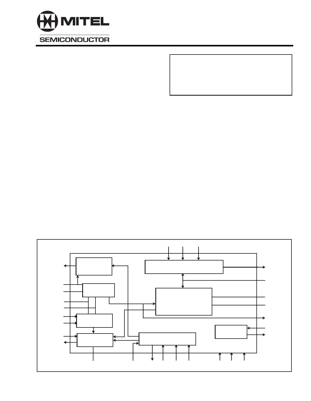
Description
The Mitel MT91600 provides an interface between a
switching system and a subscriber loop, mainly for
short loop SLIC applications. The functions provided
by the MT91600 include battery feed, programmable
constant current, 2W to 4W conversion, off-hook and
dial pulse detection, user definable line and network
balance impedance’s and the capability of
programming the audio gain externally. The device is
fabricated as a CMOS circuit in a 28 pin SSOP
package.
TD
TF
TIP
RING
RF
C3A
C3B
RV
RD
Tip Drive
Controller
Line Sense
Over-Current
Protection Circuit
Ring Drive
Controller
X3 X2 X1
Audio Gain & Network
Balance Circuit
2 W to 4 W
Conversion & Line
Impedance
Loop Supervision
Figure 1 - Functional Block Diagram
Relay
Driver
VX
VR
Z3
Z2
Z1
RLYC
RLYD
VEEGNDVDDC2BC2AC1SHKVREFIC
1
Page 2
MT91600 Preliminary Information
VDD
TD
TF
TIP
RING
VREF
RF
RV
RD
C3A
C3B
C2B
C2A
1
2
3
4
5
6
7
IC
8
9
10
11
12
13
14
28
27
26
25
24
23
22
21
20
19
18
17
16
15
VEE
GND
RLYD
RLYC
SHK
C1
X2
VR
X3
VX
X1
Z3
Z2
Z1
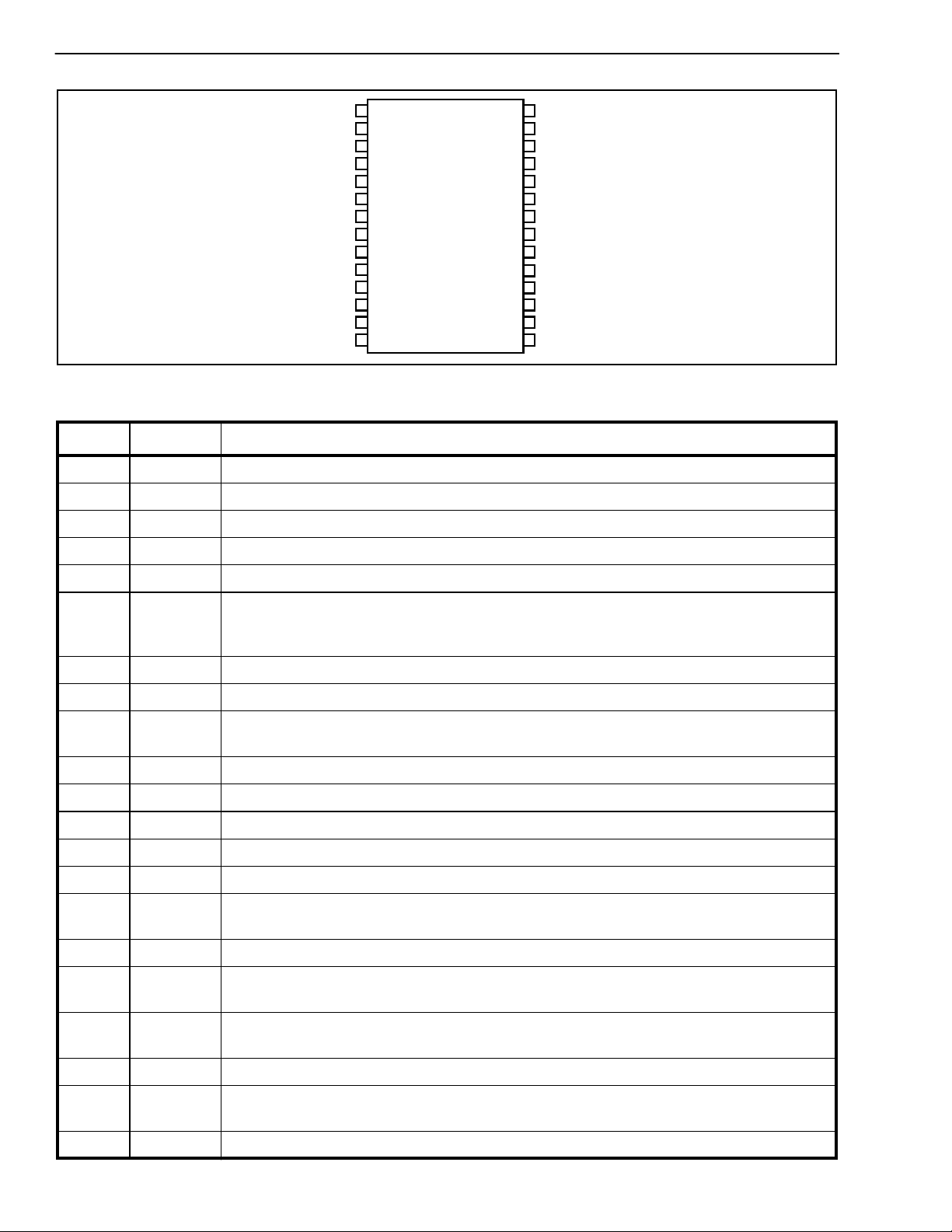
Figure 2 - Pin Connections
Pin Description
Pin # Name Description
1 VDD Positive supply rail, +5V.
2TDTip Drive (Output). Controls the Tip transistor.
3TFTip Feed. Connects to the Tip transistor and to the TIP lead via the Tip feed resistor.
4 TIP Tip. Connects to the TIP lead of the telephone line.
5 RING Ring. Connects to the RING lead of the telephone line.
6 VREF Reference Voltage (Input). This pin is used to set the subscribers loop constant
current. Changing the input voltage sets the current to any desired value within the
working limits. VREF is related to VLC.
7ICInternal Connection (Input). This pin must be connected to GND for normal operation.
8RFRing Feed. Connects to the RING lead via the Ring feed resistor.
9RVRing Voltage and Audio Feed.Connects directly to the Ring drive transistor and also to
Ring Feed via a relay.
10 RD Ring Drive (Output). Controls the Ring transistor.
11 C3A A filter capacitor for over-current protection is connected between this pin and GND.
12 C3B A filter capacitor for over-current protection is connected between this pin and GND.
13 C2B A capacitor for loop current stability is connected between this pin and C2A.
14 C2A A capacitor for loop current stability is connected between this pin and C2B.
15 Z1 Line Impedance Node 1. A resistor of scaled value "k" is connected between Z1 and
Z2. This connection can not be left open circuit.
16 Z2 Line Impedance Node 2. This is the common connection node between Z1 and Z3.
17 Z3 Line Impedance Node 3. A network either resistive or complex of scaled value "k" is
connected between Z3 and Z2. This connection can not be left open circuit.
18 X1 Gain Node 1. This is the common node between Z3 and VX where resistors are
connected to set the 2W to 4W gain.
19 VX Transmit Audio (Output). This is the 4W analog signal to the SLIC.
20 X3 Gain Node 3. This is the common node between VR and the audio input from the
CODEC or switching network where resistors are fitted to sets the 4W to 2W gain
21 VR Receive Audio (Input). This is the 4W analog signal to the SLIC.
2
Page 3

Preliminary Information MT91600
Pin Description (continued)
Pin # Name Description
22 X2 Gain Node 2. Networks, either resistive or complex, are connected between this node,
VR and GND to set the Network Balance Impedance for the SLIC.
23 C1 A filter capacitor for ring trip is connected between this pin and GND.
24 SHK Switch Hook (Output). This pin indicates the line state of the subscribers telephone.
The output can also be used for dial pulse monitoring. SHK is high in off-hook state.
25 RLYC Relay Control (Input). An active high on this pin will switch RLYD low.
26 RLYD Inverted Output of RLYC. It is used to drive the bipolar transistor that drives the relay
(see Figure 5.)
27 GND Ground. Return path for +5V and -5V. This should also be connected back to the
return path for the loop battery, LGND and relay drive ground RLYGND.
28 VEE Negative supply rail, -5V.
Functional Description
The MT91600 is the analog SLIC for use in a 4 Wire
switched system. The SLIC performs all of the
normal interface functions between the CODEC or
switching system and the analog telephone line such
as 2W to 4W conversion, constant current feed,
ringing and ring trip detection, current limiting, switch
hook indication and line and network balance
impedance setting using minimal external
components.
Refer to Figure 5 for MT91600 components
designation.
2 Wire to 4 Wire Conversion
The hybrid performs 2 wire to 4 wire conversion by
taking the 4 wire signal from an analog switch or
voice CODEC, a.c. coupled to VR, and converting it
to a 2 wire differential signal at tip and ring. The 2
wire signal applied to tip and ring by the telephone is
converted to a 4 wire signal, a.c. coupled to Vx which
is the output from the SLIC to the analog switch or
voice CODEC.
4W to 2W gain:
Gain 4 - 2 = 20*Log [0.891 * (R14 / R15)]
Impedance Programming
The MT91600 allows the designer to set the device’s
impedance across TIP and RING, (ZTR), and
network balance impedance, (ZNB), separately with
external low cost components.
For a resistive load, the impedance (ZTR) is set by
R11 and R18. For a complex load, the impedance
(ZTR) is set by R11, R18, R19 & C8 (see Figure 5.)
The network balance, (ZNB), is set by R16, R17 & C3
(see Figure 5.)
The network balance impedance should be
calculated once the 2W - 4W gain has been set.
Line Impedance
For optimum performance, the characteristic
impedance of the line, (Zo), and the device’s
impedance across TIP and RING, (ZTR), should
match. Therefore:
Gain Control
It is possible to set the Transmit and Receive gains
by the selection of the appropriate external
components.
The gains can be calculated by the formulae:
2W to 4W gain:
Gain 2 - 4 = 20*Log [ R13 / R12]
Zo = Z
TR
The relationship between Zo and the components
that set ZTR is given by the for mula:
Zo / ( R1+R2) = kZo / R11
where kZo =Z
ZLZ = R18, for a resistive load.
ZLZ = [R18 + (R19 // C8)], for a complex load.
LZ
3
Page 4

MT91600 Preliminary Information
The value of k can be set by the designer to be any
value between 20 and 250. Three rules to ensure the
correct operation of the circuit:
(A) R18 + R19 > 50kΩ
(B) R1 = R2.
(C) R11 > =50kΩ
It is advisable to place these components as close
as possible to the SLIC.
Network Balance Impedance
The network balance impedance, (ZNB), will set the
transhybrid loss performance for the circuit. The
balance of the circuit is independent of the 4 - 2 Wire
gain but is a function of the 2 - 4 Wire gain.
The method of setting the values for R16 and R17 is
given by the for mula:
R17 = [1.782 * Zo/ ( Zo+ZNB) * ( R13 / R12 )]
R17 + R16 [1 + R13 / R12]
where ZNB is the network balance impedance of the
SLIC and Zo is the line impedance.
The MT91600’s programmable current range is
between 18mA to 32mA.
Line Drivers & Overcurrent Protection
The Line Drivers control the external Battery Feed
circuit which provide power to the line and allows bidirectional audio transmission.
The loop supervision circuitry provides bias to the
line drivers to feed a constant current while the overcurrent protection circuitry prevents the ring driver
from causing the ring transistor to overload.
The line impedance presented by the Line Driver
circuitry is determined by the external network,
which may be purely resistive or complex, allowing
the circuit to be configured for use in any application.
The impedance can also be fixed to one value and
modified to look like a different value by reflecting an
impedance through the SLIC from an intelligent
CODEC or DSP module.
There is long term protection on the RING output
against accidental short circuits that may be applied
either across TIP/RING to GND or RING to GND.
This high current will be sensed and limited to a
value that will protect the circuit.
(R16 + R17) >= 50kΩ
It is advisable to place these components as close
as possible to the SLIC.
Loop Supervision & Dial Pulse
Detection
The Loop Supervision circuit monitors the state of
the phone line and when the phone goes "Off Hook"
the SHK pin goes high to indicate this state. This pin
reverts to a low state when the phone goes back "On
Hook" or if the loop resistance is too high for the
circuit to continue to support a constant current.
The SHK output can also be monitored for dialing
information when used in a dial pulse system.
Constant Current Control
The SLIC employs a feedback circuit to supply a
constant feed current to the line. This is done by
sensing the sum of the voltages across the feed
resistors, R1 and R2, and comparing it to the input
reference voltage, Vref, that determines the constant
current feed current.
In situations where an accidental short circuit occurs
either across TIP/RING to GND or RING to GND, an
excessive amount of current will flo w through the ring
drive transistor, Q3. Although the MT91600 will
sense this high current and limit it, if the power rating
of Q3 is not high enough, it may suffer permanent
damage. In this case, a power sharing resistor, R23,
can be inserted (see Figure 5) to dissipate some of
the power. Capacitor C13 is inserted to provide an
a.c. ground point. The criteria for selecting a value
for the power sharing resistor R23 can be found in
the application section of this datasheet.
Ringing and Ring Trip Detection
Ringing is applied to the line by disconnecting pin 8,
RF, from pin 9, RV, and connecting it to a ringing
source which is battery backed. This may be done by
use of an electro-mechanical relay. The SLIC is
capable of detecing an Off Hook condition during
ringing by filtering out the large A.C. component by
use of the external components connected to pin 23.
This filter allows an Off Hook condition to be
monitored at SHK, pin 24.
4
Page 5
Preliminary Information MT91600
When using DTMF signalling only i.e. pulse dialling
is not used, the capacitor, C7, can be permanently
connected to ground and does not require to be
switched out during dialling.
Power up Sequence
The circuit should be powered up in the following
order: AGND, VEE, VDD, V
BAT.
Application
The following Application section is intended to
demonstrate to the user the methods used in
calculating and selecting the external programming
components in implementing the MT91600 as an
analog line interface in a communication system.
The programming component values calculated
below results in the optimum performance of the
device.
Refer to Figure 5 for MT91600 components
designation.
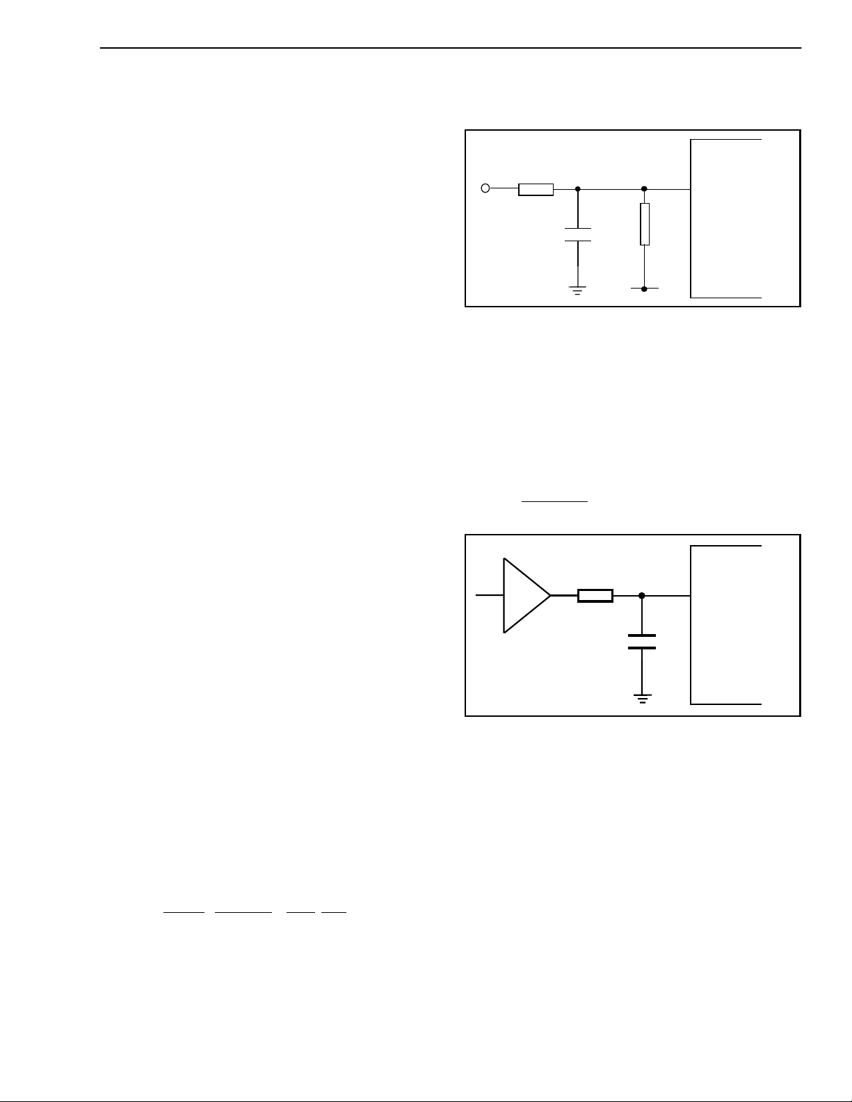
From Figure 3 with R1 = R2 = 220Ω
For I
V
LC
= 25mA, VLC = 0V, Vbat=-48V
LOOP
R3
43kΩ
R4
C9
100nF
130kΩ
V
BAT
6
V
REF
MT91600
Figure 3 - Resistor Divider
C9 is inserted to ensure pin 6, Vref, remains at a.c.
ground. 100nF is recommended.
I
can also be set by directly driving Vref with a
LOOP
low impedance voltage source. (See Figure 4). It is
recommended that a small resistor be placed in
series with the Vref pin. In this case:
I
= 1.07 * Vs where, Vs < 0
LOOP
(R1 +R2)
Component Selection
Feed Resistors (R1, R2)
The selection of feed resistors, R1 and R2, can
significantly affect the performance of the MT91600.
It is recommended that their values fall in the range
of:
200Ω <= R1 <= 250Ω
where, R1 = R2
The resistors should have a tolerance of 1% (0.15%
matched) and a power rating of 1 Watt.
Loop Current Setting (R3, R4, C9)
By using a resistive divider network, (Figure 3), it is
possible to maintain the required voltage at Vref to
set I
the following relationship:
I
LOOP
(R1 +R2)
where, F = R4 / (R4 + R3)
. The loop current programming is based on
LOOP
= - [ F * VLC + G * V
] * Ko * H
BAT
G = R3 / (R4 +R3)
Ko= 200000 / (200000 + (R4//R3) )
H = 1.07
I
is in Ampere
LOOP
2kΩ
Vs
C9
100nF
6
V
REF
MT91600
Figure 4 - Direct Voltage
Calculating Component Values For AC
Transmission
There are five parameters a designer should know
before starting the component calculations. These
five parameters are:
1) characteristic impedance of the line Z
2) network balance impedance Z
NB
o
3) value of the feed resistors (R1 and R2)
4) 2W to 4W transmit gain
5) 4W to 2W receive gain
The following example will outline a step by step
procedure for calculating component values. Given:
5
Page 6

MT91600 Preliminary Information
Zo = 600Ω, ZNB= 600Ω, R1=R2= 220Ω
Gain 2 - 4 = -1dB, Gain 4 - 2 = -1dB
Step 1: Gain Setting (R12, R13, R14, R15)
Gain 2 - 4 = 20 Log [ R13 / R12]
-1 dB = 20 Log [R13 / R12]
∴ R12 = 112.2kΩ, R13 = 100kΩ.
Gain 4 - 2 = 20 Log [0.891 * [R14 / R15)]
-1 dB = 20 Log [0.891 * [R14 / R15)]
∴ R14 = 100kΩ, R15 = 100kΩ.
Step 2: Impedance Matching (R11, R18, R19, C8)
a) Zo / ( R1+R2) = kZo / R11
600/(220+220) = (k*600)/R11
let k = 125
∴ R11 = 55kΩ.
b) In general,
Given Zo = 220Ω + (820Ω // 120nF)
Zo / ( R1+R2) = kZo / R11 (Equation 1)
where, kZo = [R18 + (R19 // C8)]
Choose a standard value for C8 to find a suitable
value for k.
Since 1nF exists, let C8 = 1nF then,
k = 120nF / C8
k = 120nF / 1nF
∴ k =120
R18 = k * 220Ω
R18 = 120 * 220Ω
R18 = 26400
R19 = k * 820Ω
R19 = 120 * 820
R19 = 98400
∴ R18 = 26k4Ω, R19 = 98k4Ω
kZo =Z
where:
ZLZ = R18, for a resistive load.
ZLZ = [R18 + (R19 // C8)], for a complex load.
Since we are dealing with a resistive load in this
example ZLZ = R18, and therefore:
kZo = R18
(125 * 600)= R18
∴ R18 = 75kΩ.
Step 3: Network Balance Impedance (R16, R17)
R17 = [1.782 * Zo/ ( Zo+ZNB) * ( R13 / R12 )]
R17 + R16 [1 + R13 / R12)]
R17 = 0.4199
R17 + R16
set R17 = 100kΩ, R16 becomes 138kΩ.
∴ R16 = 138kΩ, R17 = 100kΩ.
Complex Line Impedance, Z
LZ
o
From (Equation 1)
R11 = k * (R1 + R2)
R11 = 120 * (220Ω + 220Ω)
∴ R11 = 52k8Ω
Power Sharing Resistor (R23)
To determine the value of R23, use the following
equations:
R23(max)= |Vbat(min)| - 100 - (2*R2 + Lr + DCRP)
30mA
R23(min)= |Vbat(max)| - Pd(max) - R2
40mA 1.6mA
where,
Vbat(min/max) = the expected variation of Vbat.
R2 = the feed resistor.
Lr = maximum DC loop resistance.
DCRP = DC resistance of the phone set.
Pd(max) = the maximum power dissipation of the
ring drive transistor Q3.
In situations where the characteristic impedance of
the line Zo is a complex value, determining the
component values for impedance matching (R11,
R18, R19, C8) is as follows:
6
If R23(max) > R23(min), then set R23 to be the
geometric center:
R23 = Square Root (R23(max) * R23(min))
Page 7

Preliminary Information MT91600
If R23(max) < R23(min), then a violation has
occurred. Pd(max) will have to be increased.
A numerical example:
Given:
R2 = 220Ω
Lr = 325Ω (2.5km of 28 gauge wire, averaged at
65Ω/km)
DCRP = 200Ω
Pd(max) = 1.5W
Vbat = -48V +/- 10% (i.e. -43V to -53V)
Therefore:
R23(max) = (43/30mA) - 100 - (2 * 220 + 325 + 200)
= 1433.3 - 100 - 965
R23(max) = 368.3Ω
R23(min) = (53/40mA) - (1.5/1.6mA) - 220
= 1325 - 937.5 - 220
R23(min) = 167.5 Ω
R23 = Square Root ( 368.3 * 167.5 )
R23 = 248.4Ω
7
Page 8

MT91600 Preliminary Information
VEE
VDD
C7
C6
K1b
727281
VRLY
K1
RLYC
Q4
SHK
C4
VDD
VEE GND IC C1
SHK
24
RLYC
25
26
RLYD
D1
V
LC
V
D2a
BAT
R3
VREF
6
Q1
C9
C12
TD
2
R4
V
BAT
23
X2
VR
X3
VX
X1
22
21
20
19
18
R14
R16
C11
R13
R15
C3
R17
VRIN
VX
D2b
R22
TF
3
MT91600
R12
R1
TIP
RING
R5
~
90 Vrms
V
BAT=-48V
Q3
PR1
K1a
R2
R9
V
BAT
D3a
R6
R8
R21
R20
C5
VDD
D3b
R7
TIP
4
RING
5
RF
8
9
RV
RD C3A C3B C2B C2A
10
Q2
C1
C10
C2
17
Z3
Z2
16
Z1
15
14131211
R10
Resistive Load Z
Z
LZ
R11
Impedance Z
Complex Load Z
o
LZ
o
R18
C13
R23
V
BAT
R18
R19
C8
Figure 5 - Typical application
8
Page 9

Preliminary Information MT91600
Component List* for a Typical Application with a Resistive 600Ω Line Impendance - Refer to
Figure 5 for component designation and recommended configuration
Resistor Values
R1 220Ω 1% (0.15% matched), 1W R2 220Ω 1% (0.15% matched), 1W
R3 43kΩ R4 130kΩ
R5 220Ω R6 75kΩ
R7 3kΩ R8 1kΩ
R9 1kΩ R10 560kΩ
R11 55kΩ R12 112kΩ
R13 100kΩ R14 100kΩ
R15 100kΩ R16 138kΩ
R17 100kΩ R18 75kΩ
R19 0Ω R20 2kΩ
R21 2kΩ R22 1kΩ
R23 248Ω
Capacitor Values
C1 100nF, 5% C2 300nF, 5%
C3 100pF, 5% C4 33nF, 20%
C5 3.3nF, 5% C6 1uF, 20%, 16V
C7 100nF, 20% C8 0F
C9 100nF, 20% C10 100nF, 5%
C11 47pF, 20% C12 33nF, 10%
C13 100nF 20%
Diodes and Transistors
D1 BAS16 or equivalent D2a/b BAV99 dual diode or equivalent
D3a/b BAV99 dual diode or equivalent Q1 2N2222 or MPSA42 or MMBTA42
Q2 2N2907 or MPSA92 or MMBTA92 Q3 2N2222 or MPSA42 or MMBTA42
Q4 2N2907 or MPSA92 or MMBTA92
Note: All resistors are 1/4 W, 1% unless otherwise indicated.
*Assumes Zo = ZNB = 600Ω, Gain 2 - 4 = -1dB, Gain 4 - 2 = -1dB.
Decoupling capacitors, (1uF, 100V, 20%), can be added to VDD, VEE, V
PSRR performance.
BAT
and V
to provide improved
RLY
K1 = Electro-mechanical relay, 5V, DPDT/2 FORM C
PR1 = This device must always be fitted to ensure damage does not occur from inductive loads.For
simple applications, PR1 can be replaced by a single TVS, such as 1.5KE220C, across tip and ring. For
applications requiring lightning and mains cross protection further circuitr y will be required and the following
protection devices are suggested: P2353AA, P2353AB (Teccor), THBT20011, THBT20012, THBT200S (SGSThomson), TISP2290, TSSP8290L (T.I.)
9
Page 10

MT91600 Preliminary Information
Absolute Maximum Ratings*
Parameter Sym Min Max Units Comments
.
1 DC Supply Voltages V
V
V
DD
EE
BAT
-0.3
-6.5
-80
+6.5
+0.3
+0.3
V
V
V Limited by the Drive
transistor, Q3.
2 Ringing Voltages Vring 100 Vrms Superimposed on V
3 Voltage setting for Loop Current V
4 Overvoltage Tip/GND Ring/GND,
REF
-20 +0.3 V Note 1
200 V MAX 1ms (with power on)
BAT
Tip/Ring
5 Ringing Current Iring 30 mA. RMS
6 Ring Ground over-current 45 mA Note 2
7 Storage Temp Tstg -65 +150 ˚C
8 Package Power Dissipation Pdiss 0.10 W +85˚C max, V
BAT
= -48V
9 ESD Rating 500 V Human Body Model
Note 3
*Exceeding these values may cause permanent damage. Functional operation under these conditions is not implied.
Note 1: Voltage at Vref pin set by VLC and potential divider.
Note 2: Tip and Ring must not be shorted together and to ground at the same time.
Note 3: The device contains circuitry to protect the inputs from static voltage up to 500V. However, precautions should be taken to avoid
static charge build up when handling the device.
Recommended Operating Conditions
Parameter Sym Min Typ
‡
Max Units Test Conditions
1 Operating
Supply Voltages
2 Ringing Voltage Vring 0 50 V
V
V
V
DD
EE
BAT
4.75
-5.25
-72
5.00
-5.00
-48
5.25
-4.75
-22
V
V
V
RMS
3 Voltage setting for Loop Current VREF -10.3 V I
4 Operating Temperature To -40 +25 +85 ˚C
‡ Typical figures are at 25˚C with nominal supply voltages and are for design aid only
†Electrical Characteristics are over Recommended Operating Conditions unless otherwise stated.
‡Typical figures are at 25°C with nominal + 5V supplies and are for design aid only.
Note 4: 16 to 68 Hz superimposed on a V
BAT
.
Note 4
= 25mA,
LOOP
R1=R2=220Ω
V
= -48V
BAT
10
Page 11

Preliminary Information MT91600
DC Electrical Characteristics
†
Characteristics Sym Min Typ‡Max Units Test Conditions
1 Supply Current I
I
I
BAT
DD
EE
25
11
8.5
45
mA
mA
mA
2 Power Consumption PC 60 90 mW Standby/Active
3 Constant Current Line
Feed
4 Programmable Loop
I
LOOP
I
LOOP
22 25 28 mA V
18 32 mA
= -10.3V
REF
Test circuit as Fig. 6
V
= -48V
BAT
Current Range
5 Operating Loop
(inclusive of Telephone
Set)
6 Off Hook Detection
Threshold
R
LOOP
1200
450
Ω
Ω
SHK 20 mA V
I
LOOP
V
BAT
I
LOOP
V
BAT
REF
V
BAT
= 18mA
= -48V
= 18mA
= -22V
= -10.3V
= -48V
See Note 5. I
7RLYC
Input Low Voltage
Input High Voltage
Vil
Vih
2.0
0.4 0.7 V
V
lil = 50µA
lih = +50µA
LOOP
= 25mA
8 SHK
Output Low Voltage
Output High Voltage
8 Dial Pulse Distortion ON
OFF
†
Electrical Characteristics are over Recommended Operating Conditions unless otherwise stated.
‡
Typical figures are at 25°C with nominal +5V and are for design aid only.
Note 5: Off hook detection is related to loop current.
Vol
Voh
2.7
+4
+4
0.4 V
V
ms
ms
Lol = 8mA
Loh = -0.4mA
11
Page 12

MT91600 Preliminary Information
AC Electrical Characteristics
Characteristics Sym Min Typ
†
‡
Max Units Test Conditions
1 Ring Trip Detect Time Tt 100 300 mS
2 Output Impedance at VX 10 Ω
3 Gain 4-2 @ 1kHz -1.3 -1 -0.8 dB Note 6
Test circuit as Fig. 8
4 Gain Relative to 1kHz ±0.15 dB 300Hz - 3400Hz
5 Transhybrid Loss THL 20 25 dB Note 6
300Hz - 3400Hz
Test circuit as Fig. 8
6 Gain 2-4 @ 1kHz -1.3 -1 -0.8 dB Note 6
Test circuit as Fig. 7
7 Gain Relative to 1kHz ±0.15 dB 300Hz to 3400Hz
8 Return Loss at 2-Wire RL 20 30
dB
Note 6
300Hz - 3400Hz
Test circuit as Fig. 10
9 Total Harmonic Distortion
@2W
@VX
THD
0.3
0.3
1.0
1.0
%
%
3dBm, 1kHz @ 2W
1Vrms, 1KHz @ 4W
10 Common Mode Rejection
2 wire to Vx
CMR 35 42 dB Input 0.5Vrms, 1KHz
Test circuit as Fig. 9
11 Longitudinal to Metallic Balance LCL 55 dB 200Hz to 3400Hz
Test circuit as Fig. 9
12 Metallic to Longitudinal Balance 58
48
13 Idle Channel Noise
Nc
@2W
@VX
14 Power Supply Rejection
PSRR
12
12
dB
dB
dBrnC
dBrnC
200Hz to 1000Hz
1000Hz to 3400Hz
Cmessage Filter
Cmessage Filter
Ratio at 2W and VX
Vdd
V ee
†
Electrical Characteristics are over Recommended Operating Conditions unless otherwise stated.
‡
Typical figures are at 25°C with nominal +5V and are for design aid only.
Note 6: Assumes Zo = ZNB = 600Ω and both transmit and receive gains are programmed externally to -1dB, i.e. Gain 2-4 = -1dB , Gain 4-2
= -1dB.
23
23
dB
dB
0.1Vp-p @ 1kHz
Mechanical Information
Refer to the latest copy of the Mitel data book for details of the outline for the 28 Pin SSOP package.
12
Page 13

Preliminary Information MT91600
Test Circuits
Figures 6,7,8,9,10 are for illustrating the principles involved in making measurements and do not necessarily
reflect the actual method used in production testing.
TIP
I
Loop
Z
o
RING
SLIC
6
R4
V
BAT
R3
C9
V
LC
Figure 6 - Loop current programming
20
TIP
Z
o
__
2
SLIC
o
RING
V
TR
V
S
~
Z
__
2
19
18
17
R15
R13
R12
V
X
Gain = 20*Log(VX/VTR)
Gain = 20*Log(VTR/VS)
THL = 20*Log(VX/VS)
Figure 7 - 2-4 Wire Gain
19
TIP
22
21
o
RING
V
TR
Z
SLIC
20
R16 R17
C11
R14
Figure 8 - 4-2 Wire Gain & Transhybrid Loss
R15
V
~
X
C3
V
S
13
Page 14

MT91600 Preliminary Information
V
S
~
Long. Bal. = 20*Log(VTR/VS)
CMR = 20*Log(VX/VS)
R
V
S
~
R
R15
V
X
__
__
TIP
Z
o
2
V
TR
Z
o
2
RING
SLIC
20
19
Figure 9 - Longitudinal Balance & CMR
20
TIP
Z
o
V
Z
RING
SLIC
17
16
15
R15
R19
R18
C8
R11
Gain = 20*Log(2*VZ/VS)
Figure 10 - Return Loss
14
Page 15

Pin 1
Package Outlines
E
A
L
H
e
D
A
2
A
1
B
Notes:
1) Not to scale
2) Dimensions in inches
3) (Dimensions in millimeters)
4) Ref. JEDEC Standard M0-150/M0118 for 48 Pin
5) A & B Maximum dimensions include allowable mold flash
C
20-Pin 24-Pin 28-Pin 48-Pin
Dim
Min Max Min Max Min Max Min Max
A 0.079
(2)
A10.002
(0.05)
B 0.0087
(0.22)
C 0.008
D 0.27
(6.9)
E 0.2
(5.0)
e 0.025 BSC
A20.065
(1.65)
H 0.29
(7.4)
L 0.022
(0.55)
0.013
(0.33)
(0.21)
0.295
(7.5)
0.22
(5.6)
(0.635 BSC)
0.073
(1.85)
0.32
(8.2)
0.037
(0.95)
- 0.079
0.002
(0.05)
0.0087
(0.22)
0.31
(7.9)
0.2
(5.0)
0.025 BSC
(0.635 BSC)
0.065
(1.65)
0.29
(7.4)
0.022
(0.55)
(2)
0.013
(0.33)
0.008
(0.21)
0.33
(8.5)
0.22
(5.6)
0.073
(1.85)
0.32
(8.2)
0.037
(0.95)
0.002
(0.05)
0.0087
(0.22)
0.39
(9.9)
0.2
(5.0)
0.025 BSC
(0.635 BSC)
0.065
(1.65)
0.29
(7.4)
0.022
(0.55)
0.079
(2)
0.013
(0.33)
0.008
(0.21)
0.42
(10.5)
0.22
(5.6)
0.073
(1.85)
0.32
(8.2)
0.037
(0.95)
0.095
(2.41)
0.008
(0.2)
0.008
(0.2)
0.62
(15.75)
0.291
(7.39)
0.025 BSC
(0.635 BSC)
0.089
(2.26)
0.395
(10.03)
0.02
(0.51)
0.110
(2.79)
0.016
(0.406)
0.0135
(0.342)
0.010
(0.25)
0.63
(16.00)
0.299
(7.59)
0.099
(2.52)
0.42
(10.67)
0.04
(1.02)
Small Shrink Outline Package (SSOP) - N Suffix
General-11
Page 16

http://www.mitelsemi.com
World Headquarters - Canada
Tel: +1 (613) 592 2122
Fax: +1 (613) 592 6909
North America Asia/Pacific Europe, Middle East,
Tel: +1 (770) 486 0194 Tel: +65 333 6193 and Africa (EMEA)
Fax: +1 (770) 631 8213 Fax: +65 333 6192 Tel: +44 (0) 1793 518528
Fax: +44 (0) 1793 518581
Information relating to products and services furnished herein by Mitel Corporation or its subsidiaries (collectively “Mitel”) is believed to be reliable. However, Mitel assumes no
liability for errors that may appear in this publication, or for liability otherwise arising from the application or use of any such information, product or service or for any infringement of
patents or other intellectual property rights owned by third parties which may result from such application or use. Neither the supply of such information or purchase of product or
service conveys any license, either express or implied, under patents or other intellectual property rights owned by Mitel or licensed from third parties by Mitel, whatsoever.
Purchasers of products are also hereby notified that the use of product in certain ways or in combination with Mitel, or non-Mitel furnished goods or services may infringe patents or
other intellectual property rights owned by Mitel.
This publication is issued to provide information only and (unless agreed by Mitel in writing) may not be used, applied or reproduced for any purpose nor form par t of any order or
contract nor to be regarded as a representation relating to the products or services concerned. The products, their specifications, services and other information appearing in this
publication are subject to change by Mitel without notice. No warranty or guarantee express or implied is made regarding the capability, performance or suitability of any product or
service. Information concerning possible methods of use is provided as a guide only and does not constitute any guarantee that such methods of use will be satisfactory in a specific
piece of equipment. It is the user’s responsibility to fully determine the performance and suitability of any equipment using such information and to ensure that any publication or
data used is up to date and has not been superseded. Manufacturing does not necessarily include testing of all functions or parameters. These products are not suitable for use in
any medical products whose failure to perform may result in significant injury or death to the user. All products and materials are sold and services provided subject to Mitel’s
conditions of sale which are available on request.
M Mitel (design) and ST-BUS are registered trademarks of MITEL Corporation
Mitel Semiconductor is an ISO 9001 Registered Company
Copyright 1999 MITEL Corporation
All Rights Reserved
Printed in CANADA
TECHNICAL DOCUMENTATION - NOT FOR RESALE
 Loading...