

Page 1
CMOS
MT9126
Quad ADPCM Transcoder
Preliminary Information
Features
• Full duplex transc ode r with four e ncod e
channels a nd fou r de code c hanne ls
• 32 kb/s, 24 kb/s and 16 kb/s ADPCM coding
complying with ITU-T (previously CCITT) G.726
(without 40 kb/s), and ANSI T1.303-1989
• Low power o perat ion, 25 m W ty pical
• Asynchronous 4.096 M Hz m aster clock
operation
• SSI and ST-BUS interface options
• Transparent PCM b ypass
• Transparent ADP CM bypa ss
• Linear PCM cod e
• No microprocessor control requi red
• Simple inter face t o Code c devi ces
• Pin select a ble µ−Law or A-Law o perat ion
• Pin selectable ITU-T or signed magnitude PCM
coding
• Single 5 vol t pow er suppl y
Applications
• Pair gain
• Voice mail systems
• Wireless telephony systems
ISSUE 2 May 1995
Ordering Information
MT9126AE 28 Pin Plastic D IP
MT9126AS 28 Pin SOIC
-40 °C to +85 °C
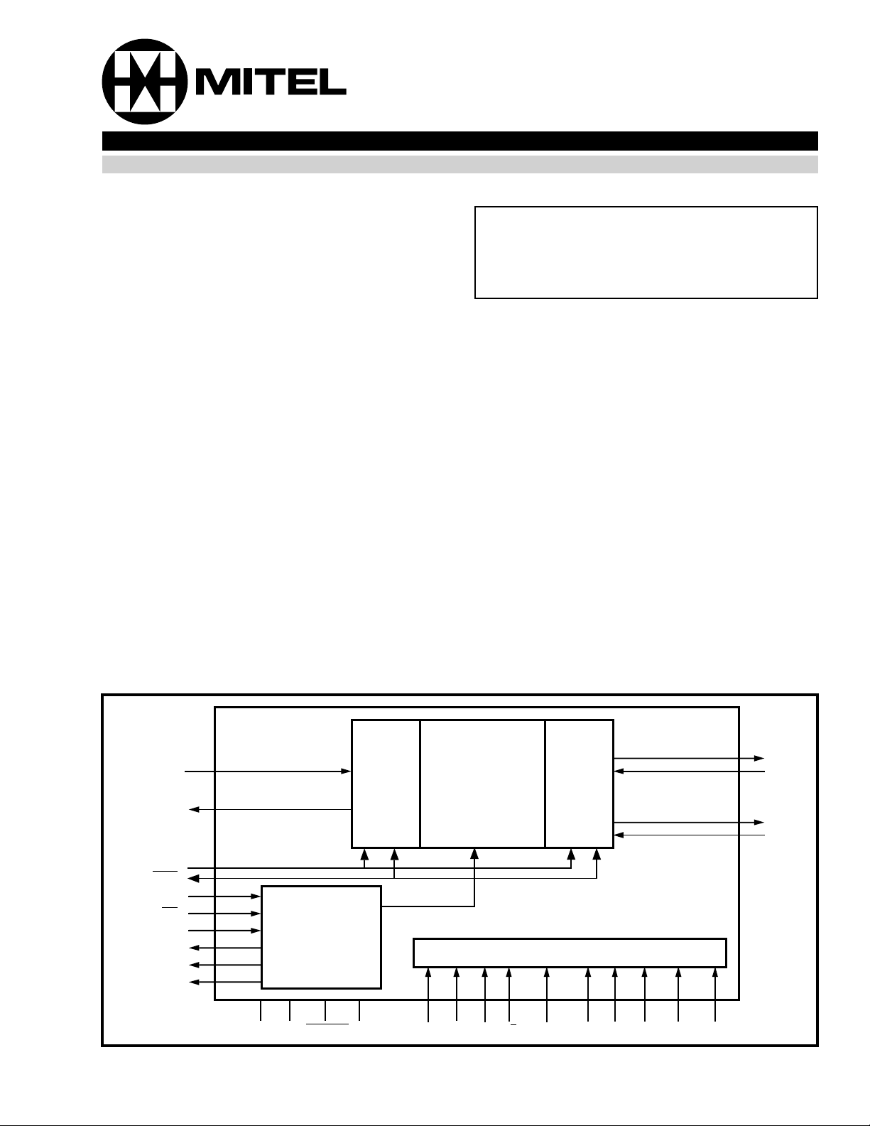
Description
The Quad ADPCM Transcoder is a low power,
CMOS device capable of four encode and four
decode functions per frame. Four 64 kbit/s PCM
octets are co mpressed into fou r 32, 2 4 or 16 kbit/s
ADPCM words, and four 32, 24 or 16 kbit/s ADPCM
words are expanded into four 64 kbit/s PCM octets.
The 32, 24 and 16 kbit/s ADPCM transcoding
algorithms utilized conform to ITU-T
Recommendation G.726 (excluding 40 kbit/s), and
ANSI T1.303 - 1 989 .
Switching, on-the-fly, between 32 kbit/s and 24 kbit/s
ADPCM, is possible by controlling the appropriate
mode select (MS1 - MS6) control pins. All optional
functions of the device are pin selectable allowing a
simple interface to industry standard codecs, digital
phone devices and Layer 1 transceivers. Linear
coded PCM is provided to facilitate external DSP
functions .
ADPCMi
ADPCMo
ENB1
ENB2/F0od
BCLK
F0i
MCLK
C2o
EN1
EN2
Timing
VDD VSS PWRDN
Full Duplex
ADPCM
I/O
Quad
PCM
I/O
Transcoder
Control Decod e
IC MS1 MS2
FORMAT MS5MS4MS3 MS6 LINEAR SEL
A/µ
Figure 1 - Functional Block Diagram
PCMo1
PCMi1
PCMo2
PCMi2
8-33
Page 2
MT9126 Preliminary Information
EN1
MCLK
F0i
C2o
BCLK
PCMo1
PCMi1
VSS
LINEAR
ENB2/F0od
ENB1
PCMo2
PCMi2
SEL
1
2
3
4
5
6
7
8
9
10
11
12
13
14
28
27
26
25
24
23
22
21
20
19
18
17
16
15
EN2
MS6
MS5
MS4
ADPCMo
ADPCMi
VDD
MS3
MS2
MS1
IC
PWRDN
FORMAT
A/µ
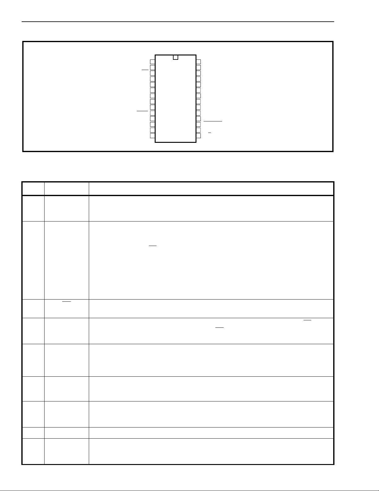
Figure 2 - Pin Connections
Pin Description
Pin # Name Description
1 EN1 Enable Strobe 1 (Output). This 8 bit wide, active high strobe is active during the B1
PCM channel in ST-BUS mode. Becomes a single bit, high true pulse when LINEA R=1.
In SSI mode this output is high impedance.
2 MCLK Master Clock (in pu t). This is a 4.096 MHz (minim um ) input clock utilized by the
transcoder function; it must be supplied in both ST-B US and SSI modes of operation.
In ST-BUS mode the C4
ST-BUS clock is applied to this pin. This synchronous clock is
also used to control the data I/O flow on the PCM and ADP CM input/out put pins
according to ST-BUS requirements.
In SSI mode this master clock input is derived from an external sour ce and may be
asynchronous with respect to the 8 kHz frame. MCLK rates greater than 4.096 MHz are
acceptable in this mode since the data I/O rate is governed by BCLK.
3F0i
4 C2o 2.048 MHz Clock (Ou tput). This ST-BU S mode bit clock output is the MCLK (C4
Frame Pulse (Input). Frame synchronization pulse input for ST-BUS operation. SSI
operation is enabled by connecting this pin to V
SS
.
) input
divided by two, inverted, and synchronized to F0i
. This output is high-impedance during
SSI operation.
5 BC LK Bit Clock (In put). 128 kHz to 4096 kHz bit clock input for both PCM and ADPCM p orts;
used in SSI mode only. The falling edge of this clock latches data into ADPCMi, PCM i1
and PCMi2. The rising edge clocks data out on ADPCMo, PCMo1 and PCMo2. This input
must be tied to V
for ST-BUS operation.
SS
6 PCMo1 Serial P CM Stream 1 (Outpu t). 128 kbit /s to 4096 kbit/s seri al companded/ linear PCM
output stream. Data are clocked out by rising edge of BCLK in SSI mode. Clocked out by
MCLK divided by two in ST-B US mode. See Figure 1 4.
7 PCMi1 Serial PCM Stream 1 (Input). 128 kbit/s to 4096 kbit/s serial companded/line ar PCM
input stream. Data are clocked in on falling edge of BCLK in SSI mode. Clocked in at the
3/4 bit position of MCLK in ST-B US m ode. See Figure 14.
8V
SS
Digital Groun d. Nomi nally 0 volts.
9 LINEAR Linear PCM Selec t (Inpu t ). When tied to V
bit linear PCM. Linear PCM operates only at a bit rate of 2048 kbit/s. Companded PCM is
selected when this pin is tied to V
8-34
SS
the PCM I/O ports (PCM 1, PCM 2) are 16-
DD
. See Figures 5 & 8.
Page 3
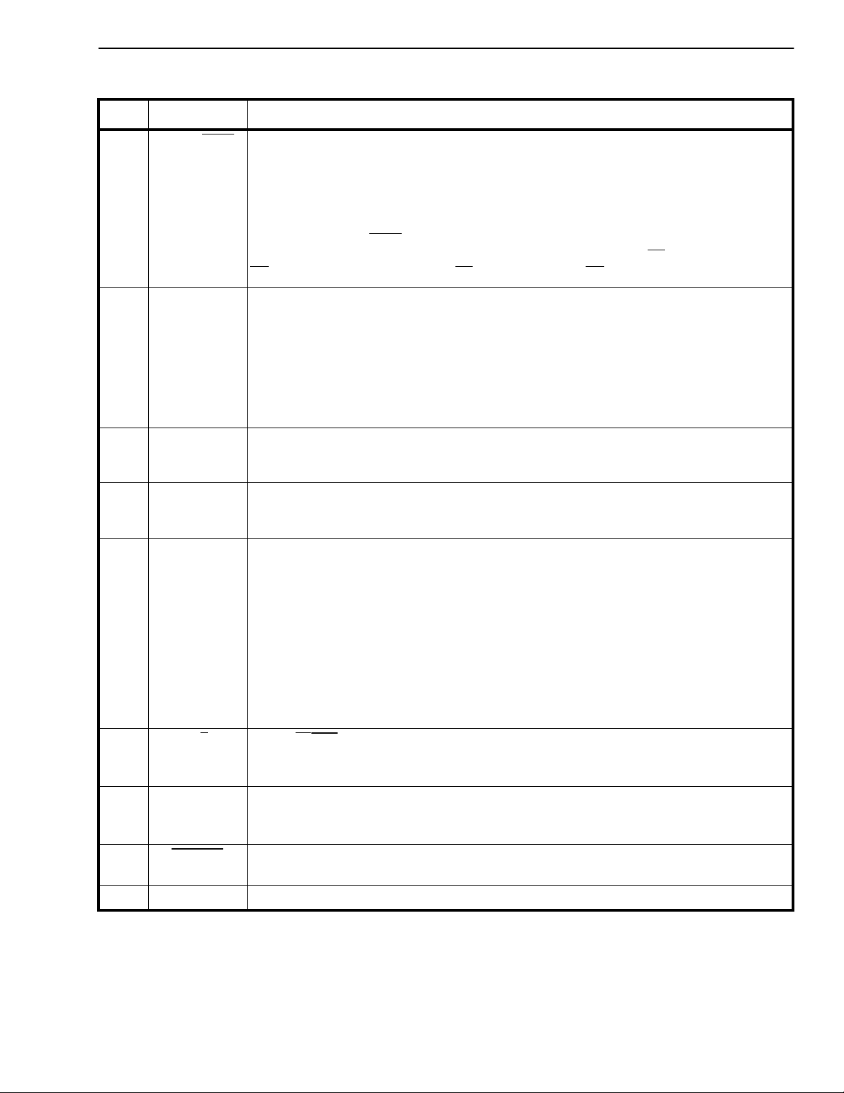
Preliminary Information MT9126
Pin Description
Pin # Name Description
10 ENB2/F0od PCM B-Chann el Enab le Strob e 2 (Input) / Dela yed Fr ame Pu lse (Outpu t).
SSI operation: ENB2 (Input). An 8-bit wide enable strobe input defining B2 channel
(AD)PCM data. A valid 8-bit strobe must be present at this input for SSI opera tion. See
Figures 4 & 6.
ST-BUS operation: F0od
EAR=0, this becomes a delayed frame pulse outp ut occurring 64 C4
and when LINEAR = 1 at 128 C4 clock cycles after F0i . See Figures 7, 8, 9 & 14.
F0i
(Output). This pin is a delayed frame strobe output. When LIN-
clock cycles after
11 EN B1 PCM B-Channel Enab le Strobe 1 (Inp ut).
SSI operation: An 8-bit wide enable strobe input defining B1 channel (AD)PCM dat a. A
valid 8-bit strobe must be present at this input for SSI operation.
ST-BUS operation: When tied to V
nels is enabled. When tied to V
transparent bypass of the ST-BUS D- and C- chan-
SS
the ST-BUS D-channel and C-channel output timeslots
DD
are forced to a high-impedance state.
12 PCMo2 Serial P CM Stream 2 (Outpu t). 128 kbit/s to 4096 kbit/s serial co mpanded/line ar PCM
output stream. Clocked out by rising edge of BCLK in SSI mode . Clocked out by MCLK
divided by two in ST-BUS m ode. See Figure 14.
13 PCMi2 Serial PCM Stream 2 (Input). 128 kbit/s to 4096 kbit/s serial companded/linear PCM input
stream. Data bit s are clocked in on falling edge of BCLK in SS I mode. Clo cked in at the
3/4 bit position of MCLK in ST-B US m ode. See Figure 14.
14 SEL SELECT (Input ).
PCM bypass mode: Wh en SE L=0 the PCM 1 port is selected for PC M bypass operation
and when SEL=1 the PCM2 port is selected for PCM bypass operati on.
See Figures 6 & 9.
16 kbit/s transcoding mode:
SSI Operation - in 16 kbit/s transcoding mode, the ADPCM words are assigned to the I/O
timeslot define d by ENB2 when SEL=1 and by ENB 1 when SEL= 0. See Fig ure 4.
ST-BUS operation- in 16 kbit/s transcoding mode, the ADPCM words are assigned to the
B2 timeslot when SEL=1 and to the B1 timeslot when SEL=0. See Figure 9.
15 A/µ
A-Law/µ−Law Select (Input). This input pin selects µ−Law comp anding when set to
logic 0, and A-Law companding when set t o logic 1. This control is for all channels .This
input is ignored in Linear mode during which it may be tied to V
or VDD.
SS
16 FORMAT FORMAT Selec t (Inpu t). Selects ITU-T P CM codin g when high and Sign-M agnit ude
PCM coding when low. This control is for all chann els.T his input is ignored in Linear
or VDD.
SS
17 PWRDN
mode during which it may be tied to V
Power-down (Input). An active low reset forcing the device into a low power mode
where all outputs are high-impedance and device operation is halted.
18 IC Internal Connection (Input). Tie to V
for normal operation.
SS
8-35
Page 4

MT9126 Preliminary Information
Pin Description
Pin # Name Description
19
20
21
MS1
MS2
MS3
Mode Selects 1, 2 and 3 (Inputs). Mode selects for all four encoders.
MS3
MS2 MS1 MODE
0 0 0 32 kbit/s ADPCM
0 0 1 24 kbit/s ADPCM
0 1 0 16 kbit/s ADP CM in EN1/ENB 1 when SEL =0
in EN2/ENB2 when SEL=1
0 1 1 ADPCM Bypass for 32 kbit/s and 24 kbit/s
1 0 0 ADPCM Bypass for 16 kbit/s
1 0 1 PCM Bypass (64 kbit/s) to PCM1 if SEL=0, PCM2 if SEL=1
1 1 0 Algorithm reset (IT U-T opt ional reset)
1 1 1 ADPCMo disable
22 V
DD
Positive Power Supply. Nominally 5 volts +/-10%
23 ADPCMi Serial ADPCM Stream ( Input). 128 kbit/s to 4096 kbit/s serial ADPCM word input
stream. Data bit s are clocked in on falling edge of BCLK in SS I mode and clo cke d in on
the 3/4 bit edge of MCLK in ST-BUS mod e.
24 ADPCMo Serial ADPCM Stream (Output). 128 kbit/s to 4096 kbit/s serial ADPCM word outpu t
stream. Data bits are clocked out by rising edge of BCLK in SSI mode and clocked out by
MCLK divided by two in ST-B US mode.
25
26
27
MS4
MS5
MS6
Mode Selects 4, 5 and 6 (Inputs). Mode selects for all four decoders.
MS6
MS5 MS4 MODE
0 0 0 32 kbit/s ADPCM
0 0 1 24 kbit/s ADPCM
0 1 0 1 6 kbit/s ADP CM in EN1/ENB 1 when SEL =0
in EN2/ENB2 when S EL=1
0 1 1 ADPCM Bypass for 32 kbit/s and 24 kbit/s
1 0 0 ADPCM Bypass for 16 kbit/s
1 0 1 P CM Bypass (64 kbit/s) to PCM1 if SEL=0, PCM2 if SEL=1
1 1 0 A lgo rithm reset (IT U-T opt ional reset)
1 1 1 PCMo1/2 disable
28 EN2 Enable Strobe 2 (Output). This 8 bit wide, active high strobe is acti ve during the B2
PCM channel in ST-BUS mode. Forced to high impedance when LINE AR=1.
Notes:
All unused inputs should be connected to logic low or high unless otherwise stated. All outputs should be left open circuit when not used.
All inputs have TTL compatible logic levels except for MCLK which has CMOS compatible logic levels and PWRDN
trigger compatible logic levels.
All outputs are CMOS with CMOS logic levels (See DC Electrical Characteristics).
which has Schmitt
8-36
Page 5

Preliminary Information MT9126
Functional Description
The Quad-channel ADPCM Transcoder is a low
power, CMOS device capable of four encode and
four decode operations per frame. Four 64 kbit/s
channels (PCM octets) are compressed into four 32,
24 or 16 kbit/s ADPCM channels (ADPCM words),
and four 32, 24 or 16 kbit/s ADPCM channels
(ADPCM words) are expanded into four 64 kbit/s
PCM channels (PCM octets). The ADPCM
transcoding algorithm utilized conforms to ITU-T
recommendation G.726 (excluding 40 kb/s), and
ANSI T1.303 - 1989. Switching on-the-fly between
32 and 24 kbit/s transcoding is possible by toggling
the appropriate mode select pins (supports T1
robbed-bit signalling).
All functions supported by the device are pin
selectable. The four encode functions comprise a
common group controlled via Mode Select pins MS1,
MS2 and MS3. Similarily, the four decode functions
form a second group commonly controlled via Mode
Select pins MS4, MS5 and MS6. All other pin
controls are common to the entire transcoder.
Serial (AD)PCM D ata I /O
Serial data transfer to/from the Quad ADPCM
transcoder is provided through one ADPCM and two
PCM ports (ADPCMi, ADPCMo, PCMi1, PCMo1,
PCMi2, PCMo2). Data is transferred through these
ports according to either ST-BUS or SSI
requirements. The device determines the mode of
operation by monitoring the signal applied to the F0i
pin. When a valid ST-BUS frame pulse (244nSec low
going pulse) is applied to the F0i
will assume ST-BUS operation. If F0i
continuously to V
operation. Pin functionality in each of these modes is
described in the following sub-sections.
ST-BUS Mode
During ST-BUS operation the C2o, EN1, EN2 and
outputs become active and all serial timing is
F0od
derived from the MCLK (C4
BCLK inpu t i s tie d to V
the transcoder will assume SSI
SS
. (See Figures 7, 8 & 9.)
SS
Basic Rate “D” and “C” Chan nels
pin the transcoder
is tied
) and F0i inputs while the
The device requires 25 mWatts (MCLK= 4.096 MHz)
typically for four channel transcode operation. A
minimum master clock frequency of 4.096 MHz is
required for the circuit to complete four encode
channels and four decode channels per frame. For
SSI operation a master clock frequency greater than
4.096 MHz and asynchronous, relative to the 8 kHz
frame, is allowed.
The PCM and ADPCM serial busses support both
ST-BUS and Synchronous Serial Interface (SSI)
operation. This allows serial data clock rates from
128 kHz to 4096 kHz, as well as compatibility with
Mitel’s standard Serial Telecom BUS (ST-BUS). For
ST-BUS operation, on chip channel counters provide
channel enable outputs as well as a 2048 kHz bit
clock output which may be used by down-stream
devices utilizing the SSI bus interface.
Linear coded PCM is also supported. In this mode
the encoders compress, four 14-bit, two’s
complement (S,S,S,12,...,1,0), uniform PCM
channels into four 4, 3 or 2 bit ADPCM channels.
Similarly, the decoder expands four 4, 3 or 2 bit
ADPCM channels into four 16-bit, two’s complement
(S,14,...,1 ,0), uniform PCM chann els. The da ta rate
for both ST-BUS and SSI operation in this mode is
2048 kbit/s.
In ST-BUS mode, when ENB1 is brought low,
transparent transport of the ST-BUS "Basic Rate Dand C-channels" is supported through the PCMi1
and PCMo1 pins. This allows a microprocessor
controlled device, connected to the PCMi/o1 pins, to
access the "D" and "C" channels of a transmission
device connected to the ADPCMi/o pins. When
ENB1 is brought high, the “D” and “C” channel
outputs are tristated. Basic Rate “D” and “C”
channels are not supported in LINEAR mode.(See
Figure 7.)
SSI Mode
During SSI operation the BCLK, ENB1 and ENB2/
F0od
inputs become active. The C2o, EN1, and EN2
outputs are forced to a high-impedance state except
during LINEAR operation during which the EN1
outp u t rema ins active. (See Figures 4, 5 & 6.)
The SSI port is a serial data interface, including data
input and data output pins, a variable rate bit clock
input and two input strobes providing enables for
data transfers. There are three SSI I/O ports on the
Quad ADPCM; the PCMi/o1 PCM port, the PCMi/o2
PCM port, and the ADPCMi/o port. The two PCM
ports may transport 8-bit companded PCM or 16-bit
linear PCM. The alignment of the channels is
determined by the two input strobe signals ENB1
and ENB2/F0od
strobes (ENB1 and ENB2/F0od
. The bit clock (BCLK) and input
) are common for all
8-37
Page 6

MT9126 Preliminary Information
three of the serial I/O ports. BCLK can be any
frequency between 128 kHz and 4096 kHz
synchronized to the input strobes. BCLK may be
discontinuous outside of the strobe boundaries
except when LINEAR=1. In LINEAR mode, BCLK
must be 2048 kHz and continuous for 64 cycles after
the ENB1 rising edge and for the duration of ENB2/
.
F0od
Mode Select Operation (MS1, MS2, MS3,
MS4, MS5, MS6)
Mode Select pins MS1, MS2 and MS3 program
different bit rate ADPCM coding, bypass, algorithmic
reset and disable modes for all four encoder
functions simultaneously. When 24 kbit/s ADPCM
mode is selected bit 4 is unused while in 16 kb/s
ADPCM mode all ADPCM channels are packed
contiguously into one 8-bit octet. Mode Select pins
MS4, MS5 and MS6 operate in the same manner for
the four decode functions. The mode selects must be
set up according to the timing const raints illustrated
in Figures 16 and 17.
16 kbit/s ADPCM Mode
When SEL is set to 0, the 8-bit PCM octets of the B1,
B2, B3 and B4 channels (PCMi1 and PCMi2) are
compressed into four 2-bit ADPCM words on
ADPCMo during t he EN B1 time slot i n SSI mo de a nd
during the B1 timeslot in ST-BUS mode. Similarily,
the four 2-bit ADPCM words on ADPCMi are
expanded into four 8-bit PCM octets (on PCMo1 and
PCMo2) during the ENB1/B1 times lot. (S ee Figu re s 4
& 7.)
When SEL is set to 1, The same conversion takes
place as described when SEL = 0 except that the
ENB2/B2 timeslots are utilized.
A-Law or µ-Law 8-bit PCM are received and
transmitted most significant bit first starting with b7
and ending with b0. ADPCM data are most
significant bit first starting with I1 and ending with I2.
ADPCM BYPASS (32 and 24 kbit/s)
32 kbit/s ADPCM Mode
In 32 kbit/ s ADPCM mode, the 8-bit PCM o ctets of
the B1, B2, B3 and B4 channels (PCMi1 and PCMi2)
are compressed into four 4-bit ADPCM words on
ADPCMo. C o nv e rsel y, the 4-bit ADPC M words of the
B1, B2, B3 and B4 channels from ADPCMi are
expanded into four 8-bit PCM octets on PCMo1 and
PCMo2. The 8-bit PCM octets (A-Law or µ-Law ) are
transferred most significant bit first starting with b7
and ending with b0. ADPCM words are transferred
most significant bit first starting with I1 and ending
with I4 (See Figures 4 & 7). Reference ITU-T G .726
for I-bit definition s.
24 kbit/s ADPCM Mode
In 24 kbit/s mode PCM octets are transcoded into 3bit words rather than the 4-bit words utilized in 32
kbit/s ADPCM. This is useful in situations where
lower bandwidth transmission is required. Dynamic
operation of the mode select control pins will allow
switching from 32 kbit/s mode to 24 kbit/s mode on a
frame by frame basis. The 8 bit PCM octets (A-Law
or µ-Law) are transferred most significant bit first
starting with b7 and ending with b0. ADPCM words
are transferred most significant bit first starting with
I1 and ending with I3 (I4 becomes don’t care). (See
Figures 4 & 7.)
In ADPCM bypass mode the B1 and B2 channel
ADPCM words are bypassed (with a two-frame
delay) to/from the ADPCM port and placed into the
most significant nibbles of the PCM1/2 port octets.
Note that the SEL pin performs no function for these
two modes (See Figures 6 & 9). LINEAR, FORMAT
and A/µ
In 32 kb/s ADPCM bypass mode, Bits 1 to 4 of the
B1, B2, B3 and B4 channels from PCMi1 and PCMi2
are trans parently pas sed, with a two frame delay, to
the same channels on ADPCMo. In the same
manner, the B1, B2, B3 and B4 channels from
ADPCMi are transparently passed, with a two frame
delay, to the same channels on PCMo1 and PCMo2
pins. Bits 5 to 8 are don’t care. This feature allows
two voice terminals, which utilize ADPCM
transcoding, to communicate through a system
without incurring unnecessary transcode
conversions. This arrangement allows byte-wide or
nibble-wide transport through a switching matrix.
24 kb/s ADPCM bypass mode is the same as 32 kb/s
mode bypass excepting that only bits 1 to 3 are
bypassed and bits 4 to 8 are don’t care.
pins are ignored in bypass mode.
ADPCM BYPASS (16 kbit/s)
When SEL is set to 0, only bits 1 and 2 of the B1, B2,
B3 and B4 PCM octets (on PCMi1 and PCMi2) are
bypassed, with a two frame delay, to the same
channels on ADPCMo during the ENB1 timeslot in
SSI mode and during the B1 timeslot in ST-BUS
8-38
Page 7

Preliminary Information MT9126
mode. Similarily, the four 2-bit ADPCM words on
ADPCMi are transparently bypassed, with a two
frame delay, to PCMo1 and PCMo2 during the ENB1
or B1 t i m eslot . Bits 3 - 8 are don’t c a re. (See Figures 6
& 9.)
When SEL is set to 1, the same bypass occurs as
described when SEL = 0 except that the ENB2 or B2
timeslots are utilized.
LINEAR, FORMAT and A/µ
pins are ignored in
bypass mode.
PCM BYPASS
When SEL is set to 0, the B1 and B2 PCM channels
on PCMi1 are transparently passed, with a twoframe delay, to the same channels on the ADPCMo.
Simiarily, the two 8-bit words which are on ADPCMi
are transparently passed, with a two-frame delay, to
channels B1 and B2 of PCMo1 while PCMo2 is set
to a high- impeda nce s tate.(See Figures 6 & 9.)
When SEL is set to 1, the B3 and B4 channels on
PCMi2 are transparently passed, with a two frame
delay, to the same channels on ADPCMo. Similarily,
the two 8-bit words which are on ADPCMi are
transparently passed, with a two-frame delay, to
channels B3 and B4 of PCMo2. In this case PCMo1
is always high-impedance if ENB1 = 0. If E NB1 = 1
during ST-BUS operation then the D and C channels
are active on PCMo1.
LINEAR, FORMAT and A/µ
pins are ignored in
bypass mode.
Algorithm Reset Mode
While an algorithmic reset is asserted the device will
incrementally converge its internal variables to the
'Optional reset values' stated in G.726. Algorithmic
reset requires that the master clock (MCLK) and
frame pulse (ENB1/2 or F0i
) remain active and that
the reset condition be valid for at least four frames.
Note that this is not a power down mode; see
PWRDN
for this fun c ti o n.
ADPCMo & PCMo1/2 Disable
When the decoders are programmed for PCMo1/2
disable (MS4 to MS6 set to 1) the PCMo1/2 outputs
are high impedance during the B Channel timeslots
and also, during ST-BUS operation, the D and C
channel timeslots according to the state of ENB1.
Therefore convergence is maintained. The encode
processing function and data I/O remain active.
Whenever any combination of the encoders or
decoders are set to the disable mode the following
outputs remain active. A) ST-BUS mode: ENB2/
, EN1, EN2 and C2o. Also the “D” and “C”
F0od
channels from PCMo1 and A DPCMo remain act ive if
ENB1 is set to 0. If ENB1 is brought high then
PCMo1 and ADPCMo are fully tri-stated. B) SSI
mode: When used in the 16-bit linear mode, only the
EN1 output remains active. For complet e chip power
down see PWRDN
.
Other Pin Controls
16 Bit Linear PCM
Setting the LINEAR pin to logic one causes the
device to change to 16-bit linear (uniform) PCM
transmission on the PCMi/o1 and PCMi/o2 ports.
The data rate for both S T-BUS and SSI operation in
this mode is 2048 kbit/s and all decode and encode
functions are aff ected by this pin. In SSI mode, the
input channel strobes ENB1 and ENB2/F0od
active for 8 cycles of BCLK for an ADPCM transfer.
The EN1 output is high for one BCLK period at the
end of the frame (i.e., during the 256
th
BCLK period).
In ST-BUS mode, the output strobes EN1 and ENB2/
F0od
are adjusted to accommodate the required
PCM I/O streams. The EN1 output becomes a single
bit high true pulse during the last clock period of the
frame (i.e., the 256
becomes a delayed, low true frame-pulse (F0od)
output occuring during the 64
th
bit period) while ENB2/F0od
th
bit period after the
EN1 rising edge.
Linear PCM on PCMi1 and PCMi2, are received as
14-bit, two’s complement data with three bits of sign
extension in the most significant positions (i.e.,
S,S,S,12,...1,0) for a total of 16 bits. The linear PCM
data transmitted from PCMo1 and PCmo2 are 16-bit,
two’s complement data with one sign bit in the most
significa nt p os iti o n ( i.e ., S,14,13,...1 ,0 )
remain
When the encoders are programmed for ADPCMo
disable (MS1 to MS3 set to 1) the ADPCMo output is
set to a high impedance state and the internal
encode function remains active. Therefore
convergence is maintained. The decode processing
function and data I/O remain active.
32 and 24 kbi t/s AD PCM mod e
In 32 kbit/s and 24 kbit/s linear mode, the 16-bit
uniform PCM dual-oct ets of the B1, B2, B3 and B4
channels (from PCMi1 and PCMi2) are compressed
into four 4-bit words on ADPCMo. The four 4-bit
ADPCM words of the B1, B2, B3 and B4 channels
8-39
Page 8

MT9126 Preliminary Information
from ADPCMi are expanded into four 16-bit uniform
PCM dual-octets on PCMo1 and PCMo2. 16-bit
uniform PCM are received and transmitted most
significant bit first starting with b15 and ending with
b0. ADPCM data are transferred most significant bit
first starting w ith I1 and e nding with I4 for 32 kbit/s
and ending with I3 for 24 kbit/s operation (i.e., I4 is
don’t care).(See Figures 5 & 8.)
16 kbit/sADPCM mode
When SEL is set to 0, the four, 2-bit ADPCM words
are transmitted/received on ADPCMo/i during the
ENB1 time-slot in SSI mode and during the B1
timeslot in ST-BUS mod e. When SEL is set to 1, the
four, 2-bit ADPCM words are transmitted/received
on ADPCMo /i dur ing the ENB2 time slot in SSI mode
and during the B2 timeslot in ST-BUS mode. (See
Figures 5 & 8.)
PCM Law Control (A/µ
, FORMAT)
The PCM companding/coding law invoked by the
transcoder is controlled via the A/µ
and FORM AT
pins. ITU-T G.711 companding curves, µ-Law and
A-Law, are selected by the A/µ
pin (0=µ-Law;
1=A-Law). Per sample, digital code assignment can
conform to ITU-T G.711 (when FORMAT=1) or to
Sign-Magnitude coding (when FORMAT=0). Table 1
illustrates th es e ch o ice s.
FORMAT
and assuming that clocks are applied to the MCLK
and BCLK pins, the internal clocks will still not begin
to operate until the first frame alignment is detected
on the ENB1 pin for SSI mode or on the F0i
pin fo r
ST-BUS mode. The C2o clock and EN1, EN2 pins
will not start operation until a valid frame pulse is
applied to the F0i
pin. If the F0i pin remains low for
longer than 2 cycles of MCLK then the C2o pin will
top toggling and will stay low. If the F0i
pin is held
high then the C2o pin will continue to operate. In STBUS mode the EN1 and EN2 pins will stop toggling if
the frame pulse (F0i
) is not applied every frame.
Master Clock (MCLK)
A minimum 4096 kHz master clock is required for
execution of the transcoding algorithm. The
algorithm requires 512 cycles of MCLK during one
frame for proper operation. For SSI operation this
input, at the MCLK pin, may be asynchronous with
the 8 kHz frame provided that the lowest frequency
and deviation due to c lock jitter still meets the strobe
period requirement of a minimum of 512 t
25%t
(see Figure 3). For example, a system
C4P
producing large jitter values can be accommodated
by running an over-speed MCLK that will ensure a
minimum 512 MCLK cycles per frame is obtained.
The minimum MCLK period is 61 nSec, which
translates to a maximum frequency of 16.384 MHz.
Extra MCLK cycles (>512/frame) are acceptable
since the transcoder is aligned by the appropriate
strobe signals each frame.
C4P
-
01
ITU-T (G.711)
(A/µ
= 0) (A/µ = 1)
PCM Code
Sign-
Magnitude
= 0 or 1
A/µ
+ Full Scale 1111 1111 1 000 00 00 1010 1010
+ Zero 1 000 0000 1111 1111 1101 0101
- Zero 0000 0000 0111 1111 0101 0101
- Full Scale 0 111 1111 0000 0000 0010 1010
Table 1 - Companded PCM
Power Down
Setting the PWRDN
pin low will asynchronously
cause all internal operation to halt and the device to
go to a power down condition where no internal
clocks are running. Output pins C2o, EN1, EN2,
PCMo1, PCMo2 and ADPCMo and I/O pin F0od
ENB2 are forced to a high-impedance state.
Foll owing the reset (i.e. , PWR DN
pin brought high)
ENB1
MCLK
512 t
C4P
- 25%t
C4P
Minimum
Figure 3 - MCLK Minimum Requirement
Bit Clock (BCLK)
For SSI operation the bit rate, for both ADPCM and
PCM ports, is determined by the clock input at BCLK.
BCLK must be eight periods in duration and
synchronous with the 8 kHz frame inputs at ENB1
and ENB2. Data is sampled at PCMi1/2 and at
ADPCMi concurrent with the falling edge of BCLK.
Data is available at PCMo1/2 and ADPCMo
concurrent with the rising edge of BCLK. BCLK may
be any rate between 128 kHz and 4096 kHz. For ST-
/
BUS operation BCLK is ignored (tie to V
bit rate i s in te rn a ll y s et to 2 0 48 kbit/s.
) and the
SS
8-40
Page 9

Preliminary Information MT9126
BCLK
ENB1
ENB2/F0od
PCMi/o1
PCMi/o2
32 kb/s
ADPCM i/o
24 kb/s
ADPCM i/o
16 kb/s
X = undetermined logic level output; don’t care input
Outputs high impedance outside of channel strobe boundaries
Two frame delay from data input to data output
Figure 4 - SSI 8-Bit Companded PCM Relative Timing
BCLK
EN1
(2.048 MHz only)
...
B1 B2
765 34 210
765 34 210
B3 B4
765 34 210765 34 210
1234
1234
B1
123x
B1 B2
12
123x
B3 B4
1212 12121212 12
1234
B2
123x
B1 B2 B3 B4
B3
SEL = 0
Notes:
S = 3 bits sign extension
µ−Law is 13 bit 2’s complement data (bits 0 -12)
A-Law is 12 bit 2’s compl eme nt da ta ( shifted l eft on ce and utilizing
bits 1 - 12, bit 0 not defined)
1234
B4
123x
SEL = 1
SEL for 16 kb/s only
ENB1
ENB2/F0od
SSS 12 11 10 9 8 7 6 5 4 3 2 1 0 SSS 12 11 10 9 8 7 6 5 4 3 2 1 0
PCMi/o1
B1
PCMi/o2
32 kb/s
ADPCM i/o
24 kb/s
ADPCMi/o
16 kb/s
X = undetermined logic level output; don’t care input
Outputs high impedance outside of channel strobe boundaries
Two frame delay from data input to data output
1234 1234 1234 1234
12
B
4
1
SEL = 1
B3
12 12 12
B2B3B
B1 B2
123x 123x 123x 123x
12
12 12 12
B
B2B3B
1
SEL = 0
Figure 5 - SSI 1 6-Bi t L ine ar PCM Rel a tive Timi ng
B4
B2
SSS 12 11 10 9 8 7 6 5 4 3 2 1 0
B3
1234 1234
SSS 12 11 10 9 8 7 6 5 4 3 2 1 0
B4
B3 B4
123x 123x
12
12 12 12
B
B2B3B
4
1
4
SEL = 1
SEL for 16 kb/s only
8-41
Page 10

MT9126 Preliminary Information
BCLK
ENB1
ENB2/F0od
PCMi/o1
ADPCMo/i
PCMi/o2
PCMi/o1
ADPCMo/i
PCMi/o2
765 34 210
B1 B2
765 34 210
SEL = 0
765 34 210
765 34 210
SEL = 1
B3 B4
765 34 210
123 x4 xxx
B1 B2
765 34 210
123 x4 xxx
123412341234 1234
B3 B4
123 x4 xxx
123 x4 xxx
SSI PCM
Bypass
32 kb/s using bits 1 2 3 4
24 kb/s where bit 4 = x
SSI ADPCM
Bypass
PCMi/o1
ADPCM o/i
121212121212 1212
B1 B2 B3 B4 B1 B2 B3 B4
PCMi/o2
12x xx xxx12x xx xxx
X = undetermined logic level output; don’t care input
Outputs high impedance outside of channel strobe boundaries
Two frame delay from data input to data output
Figur e 6 - SS I PC M an d ADP CM By pas s R elat iv e Tim ing
8-42
12x xx xxx
B1
12x xx xxx
SEL = 0
B3 B4
B2
SEL = 1
16 kb/s
Page 11

Preliminary Information MT9126
AAAA
AAAA
AAAA
AAAA
A
A
AAAA
AAAA
AAAAAA
AAAA
AAAA
AAAAAA
AAAA
AAAA
AAAAAA
AAAA
AAAA
AAAA
AAAA
AAAA
AAAA
AAAA
AAAA
AAAA
A
AAAA
A
A
MCLK (C4)
F0i
ENB2/F0od
C2o (output)
EN1 (output)
EN2 (output)
AAA
AAAA
AAAA
PCMi1
PCMo1
01
01
AAA
AAA
AAAA
AAAA
AAAA
AAAA
AAAA
AAAA
AAAA
76543
7654
3210
210
7654
7654
3
210
B1 B2DC
3210
7654
3210
76543210
AAA
AAAA
PCMi2
AAAA
transparent relay of D- and C- channels
AAA
AAAA
AAAA
AAA
AAAA
01
01
AAA
AAA
AAA
AAA
AAAA
AAAA
AAAA
AAAA
AAAA
PCMo2
ADPCMi
ADPCMo
AAA
AAAA
AAA
AAAA
X = undetermined logic level output; don’t care input
Outputs high impedance outside of channel boundaries
Two frame delay from data input to data output
outputs=High impedance
AAAA
AAAA
inputs = don’t care
AAAA
AAAA
AAAA
AAAA
AAAA
AAAA
when ENB1=0
AAAA
AAAA
AAAA
AAAA
AAAA
AAAA
AAAA
AAAA
AAAA
AAAA
AAAA
AAAA
7654
AAAA
D
AAAA
AAAA
AAAA
AAAA
7654
AAAA
AAAA
AAAA
3210
C
3210
32 kb/s is shown
In 24 kb/s, bit 4 becomes “X”
16 kb/s
SEL operates fo r
16 kb/s only
AAAA
AAA
7654
321
0
7654321
B3
AAAA
AAA
AAAA
AAA
7654
123 4
123 4
B1
121 21212121 21212
B1 B2 B4B3
121 21
321
0
7654321
B1
1234
B2
1234
123 41234
B3
123 41234
SEL=0 SEL=1
B2 B4B3
B1 B2 B4B3
B1 B2 B4B3
121 21
212
0
B4
0
B4
212
Figure 7 - ST-BUS 8-bit Companded PCM Relative Tim ing
8-43
Page 12

MT9126 Preliminary Information
A
A
A
A
A
A
A
A
A
A
A
A
A
A
A
A
A
A
A
A
A
A
A
A
A
A
A
A
A
A
A
A
A
A
A
A
A
A
A
A
A
A
A
A
A
A
A
A
A
A
A
A
A
A
A
A
A
A
A
A
A
A
A
A
A
A
A
A
A
A
A
A
A
A
A
A
A
A
A
A
A
A
A
A
A
A
A
AAAA
AAAA
A
AAAA
AAAA
AAAA
A
AAAA
A
A
A
A
A
A
A
A
A
A
A
A
AAAA
AAAA
AAAA
AAAA
AAAA
A
AA
AAAA
AAAA
AAAA
AAAA
AAAA
A
AA
AAAA
AAAA
AAAA
AAAA
AAAA
AAAA
AAAA
AAAA
AAAA
A
AAA
AAAA
AAAA
AAAA
AAAA
AAAA
AAAA
AAAA
AAAA
AAAA
A
AAA
AAAA
AAAA
AAAA
AAAA
A
AAA
AAAA
AAAA
AAAA
AAAA
A
AAA
MCLK (C4i)
F0i
C2o
(output)
EN1
F0od/ENB2
SSS 12 11 10 9 8 7 6 5 4 3 2 1 0
PCMi/o1
AAA
AAAA
AAA
PCMi/o2
ADPCMi/o
(32/24 kb/s)
AAA
AAA
AAA
AAA
AAA
AAA
AAAA
AAAA
AAAA
AAAA
AAAA
AAAA
AAAA
bit 4 = x at 24 kbit/s
AAAA
AAAA
AAAA
ADPCMi/o
(16 kb/s)
AAAA
AAAA
AAA
AAAA
AAAA
AAAA
AAAA
AAAA
AAAA
X = undetermined logic level output; don’t care input
Outputs high impedance outside of channel boundaries
Two frame delay from data input to data output
outputs = High impedance
AAA
AAA
inputs = don’t care
AAA
AAAA
AAAA
AAAA
AAAA
AAAA
Note: D &C channels not supported in this mode.
Figur e 8 - ST-BUS 16- bit Li nea r PC M Rela tiv e Ti ming
8-44
SSS 12 11 10 9 8 7 6 5 4 3 2 1 0
B1 B2
AAAA
AAAA
AAAA
AAAA
AAAA
AAAA
AAAA
AAAA
AAAA
AAAA
AAAA
AAAA
AAAA
AAAA
AAAA
AAAA
AAAA
AAAA
AAAA
AAAA
AAAA
AAAA
AAAA
AAAA
AAAA
AAAA
AAAA
AAAA
AAAA
AAAA
AAAA
AAAA
AAAA
AAAA
AAAA
AAAA
AAAA
AAAA
AAAA
AAAA
AAAA
AA
AA
AA
AA
AAAA
AAAA
AAAA
AAAA
AAAA
AAAA
AAAA
1234 1234 1234 123 4
B1 B2
12
12 12 12
A
B
B2B3B
A
A
A
1
SEL = 0
AAAA
AAAA
AAAA
AAAA
12
B
4
1
SEL = 1
AAAA
AAAA
AAAA
AAAA
B3
12 12 1 2
B2B3B
AAAA
AAAA
AAAA
AAAA
AAAA
AAAA
AAAA
AAAA
AAAA
AAAA
AAAA
AAAA
AAAA
AAAA
AAAA
AAAA
AAAA
AAAA
AAAA
AAAA
AAAA
AAAA
AAAA
AAAA
AAAA
AAAA
AAAA
AAAA
AAAA
AAAA
AAAA
AAAA
SSS 12 11 10 9 8 7 6 5 4 3 2 1 0 SSS 12 11 10 9 8 7 6 5 4 3 2 1 0
AAA
AAA
B4
AAA
AAA
4
AAAA
AAAA
AAAA
AAAA
AAA
AAA
AAA
AAA
AAAA
AAAA
AAAA
AAAA
AAAA
AAAA
AAAA
AAAA
B3
AAAA
AAAA
AAAA
AAAA
AAAA
AAAA
AAAA
AAAA
AAAA
AAAA
AAAA
AAAA
AAAA
AAAA
AAAA
AAAA
AAAA
AAAA
AAAA
AAAA
AAAA
AAAA
AAAA
AAAA
AAAA
AAAA
AAAA
AAAA
AAAA
AAAA
AAAA
AAAA
AAAA
AAAA
AAAA
AAAA
AAAA
AAAA
AAAA
AAAA
AAAA
AAAA
AAAA
AAAA
AAAA
AAAA
AAAA
AAAA
SEL operated for
16kb/s only
B4
AAAA
AAAA
AAAA
AAAA
AAAA
AAAA
AAAA
AAAA
AAAA
AAAA
AAAA
AAAA
AAAA
AAAA
AAAA
AAAA
AAAA
AAAA
AAAA
AAAA
AAAA
AAAA
AAAA
AAAA
AA
AA
AA
AA
AA
AA
AA
AA
AA
AA
AA
AA
Page 13

Preliminary Information MT9126
A
A
A
A
A
A
A
A
AAAA
AAAA
A
AAAA
A
A
AAAA
AAAA
AAAA
AAAA
AAAA
AAAA
AAAA
AAAA
A
AAAA
AAAA
AAAA
A
AAAA
AAAA
AAAA
A
AAAA
AAAA
AAAA
A
AAAA
AAAA
AAAAAA
AAAA
AAAAAA
A
A
A
A
A
A
A
A
A
A
AAAA
AAAA
AAAA
A
AA
AAAA
AAAA
AAAA
AAAA
AAAA
AAAA
AAAA
AAAA
AAAA
A
AAA
AAAA
AAAA
AAAA
AAAA
AAAA
AAAA
AAAA
AAAA
AAAA
A
AAA
AAAA
AAAA
AAAA
A
AA
A
A
MCLK
F0i
ENB2/F0od
C2o
EN1 (output)
EN2 (output)
AAA
AAAA
AAAA
AAAA
PCMi1
AAA
AAAA
AAAA
AAAA
A
A
7 6 5 4 3 2 1 0 7 6 5 4 3 2 1 00 1 7 6 5 4 3 2 1 0
P
C
M
B
y
p
a
s
s
A
D
P
C
M
B
y
p
a
s
s
PCMo1
PCMi2
PCMo2
ADPCMi
ADPCMo
PCMi/o1
PCMi/o2
ADPCMi/o
32 kb/s
24 kb/s bit 4 = X
ADPCMi/o
(16 kb/s)
PCMi/o1
AAA
AAAA
AAAA
AAAA
AAAA
AAAA
AAA
AAAA
SEL=0
AAA
AAAA
AAAA
AAAA
AAAA
AAAA
AAAA
AAAA
AAAA
AAAA
SEL=1
AAA
AAAA
AAAA
AAAA
AAAA
AAAA
AAAA
AAAA
AAAA
AAAA
AAA
AAAA
AAAA
AAAA
A
AAA
AAAA
AAAA
AAAA
AAAA
AAAA
AAAA
AAAA
AAAA
A
AAAA
A
AAAA
7 6 5 4 3 2 1 0
AAAA
AAAA
AAAA
AAAA
AAAA
AAAA
AAAA
AAAA
AAAA
AAA
7 6 5 4 3 2 1 0
AAA
AAA
AAAA
AAAA
AAAA
AAAA
C
AAAA
AAAA
AAAA
AAAA
AAAA
AAAA
AAAA
AAAA
AAAA
AAAA
AAAA
AAAA
0 1 7 6 5 4 3 2 1 0
AAA
AAAA
AAAA
AAA
AAAA
0
1
AAA
AAAA
D
AAA
AAAA
AAAA
AAA
AAA
AAA
AAAA
AAAA
AAAA
AAAA
AAAA
AAAA
AAAA
AAAA
AAAA
AAAA
AAA
AAA
AAA
01
AAAA
AAAA
AAAA
DC
CD
AAA
AAAA
AAAA
AAA
01
01
AAA
AAA
AAA
AAAA
AAAA
AAAA
AAAA
AAAA
AAAA
7 6 5 4 3 2 1 0
AAA
AAA
AAA
7 6 5 4 3 2 1 0
B1 B2DC
7 6 5 4 3 2 1 0 7 6 5 4 3 2 1 00 1 7 6 5 4 3 2 1 0
7 6 5 4 3 2 1 0 7 6 5 4 3 2 1 0
AA
B3
AA
7 6 5 4 3 2 1 0 7 6 5 4 3 2 1 0
B4
7 6 5 4 3 2 1 0 7 6 5 4 3 2 1 00 1 7 6 5 4 3 2 1 0
B1/B3 B2/B4DC
7 6 5 4 3 2 1 0 7 6 5 4 3 2 1 0
B2B1
1 2 3 4
B3 B4
AA
AA
AA
AA
1 2 3 4
xxxx
xxx
1 2 3 4
1 2 3 4
x
1 2 3 4 1 2 3 4 1 2 3 4 1 2 3 4
B1 B2
SEL=0
B1
B2 B4B3
1 2 1 2 1 2 1 2
B1
1 2 x x x x x x
B3 B4
SEL=1
B1 B2 B4B3
1 2 1 2 1 2 1 2
B2
1 2 x x x x x x
xxxx
xxxx
PCMi/o2
AAA
AAAA
AAAA
AAA
AAAA
AAA
AAAA
X = undetermined logic level output; don’t care input
Outputs high impedance outside of channel boundaries
Two frame delay from data input to data output
outputs = High impedance
AAAA
AAAA
inputs = don’t care
AAA
AAA
AAA
AAA
AAAA
AAAA
AAAA
AAAA
AAAA
AAAA
AAAA
AAAA
D
AAAA
AAAA
AAAA
AAAA
AAAA
AAAA
AAAA
AAAA
AAAA
AAAA
AAAA
AAAA
AAAA
AAAA
AAAA
AAAA
C
AAAA
AAAA
AAAA
AAAA
AAAA
AAAA
AAAA
AAAA
AAAA
AAAA
AAAA
AAAA
B3
AA
AA
AA
1 2 x x x x x x
AA
B4
1 2 x x x x x x
Figure 9 - ST-BUS PCM an d ADP CM B ypass Rela tive Timin g
8-45
Page 14

MT9126 Preliminary Information
A
A
A
A
A
A
A
A
A
A
A
AA
AA
Processing Delay Through the Device
In order to accommodate variable rate PCM and
ADPCM interfaces, the serial input and output
streams require a complete frame to load internal
shift registers. Internal frame alignment of the
encoding/decoding functions are taken from either of
the F0i or ENB1 & ENB2 input strobes depending
upon the device operating mode (i.e., ST-BUS or
SSI). The encoding/decoding of all channels then
takes one frame to complete before the output
buffers are loaded. This results in a two frame
transcoding delay. The two frame delay also applies
to the D and C channels and to the PCM and
ADPCM by p a s s f u n ction s . (Se e Figure 10.)
Note: When changing the relative positions of the
ENB1 and ENB2 strobes, precaution mu st be taken
to ensure that two conditions are met. They are:
1) There must be at least 512 master clock cycles
between consecutive rising edges of ENB1. This
condition also holds true for ENB2.
2) The ENB1 strobe must alternate with the ENB2
stro be .
Violation of these requirements may cause noise on
the output channels.
Applications
Figure 11 depicts an ISDN line card utilizing the
MT8910 ’U’ interface transciever and MT9126
ADPCM transcoder. This central office application
implements the network end of a Pair-Gain system.
Figure 12 shows Mitel devices used to construct the
remote Pair-Gain loop terminator.
Figure 13 depicts an ADPCM to linear PCM
converter for applications where further, value
added, functions are being performed via digital
signal processor. Access to linear coded PCM
reduces the overhead of the DSP by removing the
need for a companded to linear conversion. The
linear PCM capability of the ADPCM transcoder in
conjunction with the frame alignment signal EN1
allows direct connection to the serial port of both
Motorola and Texas Instruments Digital Signal
Processors. Daisy-chaining via the delayed frame
strobe output ensures that the ADPCM array is
distributed over the complete 2048 kbit bandwidth. If
the DSP has a second serial port then access to the
processed PCM can be had directly. For processors
with only one serial port the MT8920 connected to
the DSP parallel port will provide serial access by
parallel to serial conversion. The same daisychained arrangement of Quad ADPCM transcoders
will provide a general system resource for PCMADPCM conversion by setting the device to nonlinear operation.
frame n-1 frame n frame n+1
PCMi1/2
ADPCMo
ENB1 or ENB2
F0i
MS1 or 4
Where MS2, 3, 5, 6 = 0
This diagram shows the conversion sequence from PCM to ADPCM. The same pipelining occurs in the
reverse ADPCM to PCM direction.
Total delay from data input to data output = 2 frames.
8-46
Byte "x"
PCM Byte "X" latche d into device
during frame n-1
32 kb/s 24 kb/s 32 kb/s
PCM Byte "X" processed according
to MSn input states latched during
frame n
ADPCM Word "X" output from
Word "x"
Figure 10 - Data Throughput
device during frame n+1
Page 15

Preliminary Information MT9126
AAAA
AAAA
AAAA
AAAA
AAAA
AAAA
AAAA
AAAA
AAAA
AAAA
AAAA
AAAA
AAAA
AAAA
AAAA
AAAA
AAAA
AAAA
AAAA
AAAA
AAAA
AAAA
AAAA
AAAA
AAAA
AAAA
AAAA
AAAA
AAAA
AAAA
AAAA
AAAA
AAAA
AAAA
AAAA
AAAA
AAAA
AAAA
A
A
A
A
A
A
A
A
A
A
A
A
A
A
A
A
A
A
A
AAAA
AAAA
AAAA
AAAA
AAAA
AAAA
AAAA
AAAA
AAAA
AAAA
AAAA
AAAA
AAAA
AAAA
AAAA
AAAA
AAAA
AAAA
AAAA
AAAA
AAAA
AAAA
AAAA
AAAA
AAAA
AAAA
AAAA
AAAA
AAAA
AAAA
AAAA
AAAA
AAAA
AAAA
AAAA
AAAA
AAAA
AAAA
AAAA
AAAA
AAAA
AAAA
AAAA
AAAA
AAAA
AAAA
AAAA
AAAA
AAAA
AAAA
AAAA
AAAA
AAAA
AAAA
AAAA
AAAA
AAAA
AAAA
AAAA
AAAA
AAAA
AAAA
AAAA
AAAA
AAAA
AAAA
AAAA
AAAA
AAAA
AAAA
AAAA
AAAA
AAAA
AAAA
AAAA
AAAA
AAAA
AAAA
AAAA
AAAA
AAAA
AAAA
AAAA
AAAA
AAAA
AAAA
AAAA
AAAA
AAAA
AAAA
AAAA
AAAA
AAAA
AAAA
AAAA
AAAA
AAAA
AAAA
AAAA
AAAA
AAAA
AAAA
AAAA
AAAA
AAAA
AAAA
AAAA
AAAA
AAAA
AAAA
AAAA
AAAA
AAAA
AAAA
AAAA
AAAA
AAAA
AAAA
AAAA
AAAA
AAAA
AAAA
AAAA
AAAA
AAAA
AAAA
AAAA
AAAA
AAAA
AAAA
AAAA
AAAA
AAAA
AAAA
AAAA
AAAA
AAAA
AAAA
AAAA
AAAA
AAAA
AAAA
AAAA
AAAA
AAAA
AAAA
AAAA
AAAA
AAAA
AAAA
AAAA
AAAA
AAAA
AAAA
AAAA
AAAA
AAAA
AAAA
AAAA
AAAA
AAAA
AAAA
AAAA
AAAA
AAAA
AAAA
AAAA
AAAA
AAAA
AAAA
AAAA
AAAA
AAAA
AAAA
AAAA
AAAA
AAAA
AAAA
AAAA
AAAA
AAAA
AAAA
AAAA
AAAA
AAAA
AAAA
AAAA
AAAA
AAAA
AAAA
AAAA
AAAA
AAAA
AAAA
AAAA
AAAA
AAAA
AAAA
AAAA
AAAA
AAAA
AAAA
AAAA
AAAA
AAAA
AAAA
AAAA
AAAA
AAAA
AAAA
AAAA
AAAA
AAAA
AAAA
AAAA
AAAA
AAAA
AAAA
AAAA
AAAA
AAAA
AAAA
AAAA
AAAA
AAAA
AAAA
AAAA
AAAA
AAAA
AAAA
AAAA
AAAA
AAAA
AAAA
AAAA
AAAA
AAAA
AAAA
AAAA
AAAA
AAAA
AAAA
AAAA
AAAA
AAAA
AAAA
AAAA
AAAA
AAAA
AAAA
AAAA
AAAA
AAAA
AAAA
AAAA
AAAA
AAAA
AAAA
AAAA
AAAA
AAAA
AAAA
AAAA
AAAA
AAAA
AAAA
AAAA
AAAA
AAAA
AAAA
AAAA
AAAA
AAAA
AAAA
AAAA
AAAA
AAAA
AAAA
AAAA
AAAA
AAAA
AAAA
AAAA
AAAA
AAAA
AAA
AAA
AAA
AAA
AAA
AAA
AAA
AAA
AAA
AAA
AAA
AAA
AAA
AAA
AAA
AAA
AAA
AAA
AAA
F0i
8
9
1
0
T
F0b
C4b
DSTo
DSTi
M
F0od
LIN+
LINLOUTLOUT+
T
2
R
C4i
MT9126
PCMi1
PCMo1
PCMi2
PCMo2
F0i
MCLK
ADPCMi
ADPCMo
F0od
F0i
PCMi1
1
TR
PCMi2
PCMo1
8
R
T
F0od
F0i
F0od
F0i
F0od
C4i
PCMi1
PCMo2
C4i
PCMi2
PCMo2
C4i
PCMi1
PCMo2
C4i
PCMi2
PCMo1
1
2
PCMo1
8
F0i
MT8980
F0i
ST1i
ST1o
C4i
ST2i
DX
ST2o
Figure 11 - ISDN Line Card with 32 kbit/s ADPCM
8-47
Page 16

MT9126 Preliminary Information
3
282726
EN2
MS6
MT9126
MCLK
EN1
1
2
C4b
DSTi
F0b
MS5
F0i
3
DSTo
24232221201918
25
MS4
ADPCMi
ADPCMo
PCMo1
BCLK
C2o
4
567
5V
VDD
PCMi1
or
MT8910
MT8972
10.24 MHz
MicroController
3
3
, CS1, CS2, CS3, CS4
Static Control:
SLIC Functions
Optional QADPCM
Intel MCS- 51
Motorola SPI
Nat Semi Microwire
functional control
, RC1/2 - 8 x 2 SLIC’s
16
16 control/status lines are:
LR1/2, ESE1/2, SHK1/2
8
3
D-Channel acces s through CODEC1 Microport as well as C-
9 control lines for QADPCM, some optional
8 signals for microport are:
DATA1, DATA2, SCLK, IRQ
Channel control of MT8910/MT8972
15
16
17
IC
MS2
MS1
MS3
PWRDN
A/µ
FORMAT
Reset
1
8
VSS
LINEAR
ENB2/F0od
9
ENB1
101112
8
SEL
PCMi2
PCMo2
13
14
Serial Micro-port
5V
11
12
13
14
15
16
17
2
10
201918
MT9160
123456789
5V
11
12
13
14
15
16
17
3
10
201918
MT9160
123456789
5V
11
12
13
14
15
16
17
4
10
MT9160
M+
VBias
1
VRef
M-
VSSA
PWRSTICA/µ/IRQ
5V
Din
Dout
VDD
STB/F0i
HSPKR-
HSPKR+
CLOCKin
VSSDCSSCLK
DATA1
DATA2
201918
MT9160
123456789
Figure 12 - Pair Gain Remote Terminal utilzing Mitel Components
meter signal
I/P
120VDC ring
4
38
voltage
37
15
-24VDC
120VDC ring
DCRI
VBAT
-24VDC
DCRI
GND
voltage
16
11
13
18
19
SLIC 2
MH88622
Pair Gain
1
GND
Pins
5,8,9,17,23,32,33,36
2
20
28
39
30
40
14
21
27
5V
22
7
34
3
252616
-5V
meter signal
I/P
VX1
RF1
VR1
SLIC 1
MH88622
Pair Gain
TIP1
RF2
RING1
VX2
RF3
VR2
RG1
RG2
ESTi
ESI2
VDD
RING2
VDD
TIP2
5V
VBAT
VEE
VEE
-5V
8-48
Page 17

Preliminary Information MT9126
System Frame pulse
System 4.096MHz
MT9126
C2o F0i
MCLK (C4i)
PCMo1
PCMo2 ADPCMo
ADPCMi
PCMi1
PCMi2
LINEAR
EN1 ENB2/F0o
d
+5v
MT8920
S
T
P
A
STPA
ST-BUS
port
0
X
R
Q
S
S
F
F
IR
TI DSP
2nd serial port
if available
CLKR
CLKX
DR
DX
MT9126
C2o F0i
MCLK (C4i)
PCMo1
PCMo2 ADPCMo
ADPCMi
PCMi1
PCmi2
LINEAR
EN1 ENB2/F0o
MT9126
C2o F0i
MCLK (C4i)
PCMo1
PCmo2 ADPCMo
ADPCMi
PCMi1
PCMi2
LINEAR
EN1 ENB2/F0o
MT9126
C2o F0i
MCLK (C4i)
PCMo1
PCMo2 ADPCMo
ADPCMi
PCMi1
PCMi2
LINEAR
EN1 ENB2/F0o
d
d
d
+5v
+5v
+5v
Figure 13 - ST-BUS to DSP P latform
ADPCM BUS
8-49
Page 18

MT9126 Preliminary Information
Absolute Maximum Ratings*
Parameter Symbol Min Max Units
1 Supply Voltage V
2 Voltage on any I/O pin V
3 C o ntinuous Current on any I/O pin I
4 S torage Temperature T
5 P ackage Power Dissipat ion P
* Excee ding these values may cause pe rman ent dama ge. Functi onal operati on under these cond ition s is not implie d.
DD-VSS
| V
i
o
| I
i
o
ST
D
Recommended Operating Conditions - Voltages are with respect to ground (V
Characteristics Sym Min Typ
1 Supply Voltage V
DD
4.5 5.0 5.5 V
2 TTL Input High Voltage 2.4 V
3 TTL Input Low Voltage V
SS
4 CMOS Input High Voltage 4.5 V
5 CMO S Input Low Voltage V
6 Operat ing Temperature T
‡ Typical figures are at 25°C and are for design aid only: not guaranteed and not subject to producti on testing.
A
SS
-40 +85 °C
DC Electrical Characteristics - Voltages are with respect to ground (V
‡
Max Uni ts Test Conditions
DD
0.4 V 400mV noise margin
DD
0.5 V
) unless otherwise stated.
SS
-0.3 7.0 V
VSS-0.3 VDD+ 0.3 V
-65 150 °C
) unless otherwise stated.
SS
V 400mV noise margin
V
±20 mA
500 mW
Characteristics Sym Min Typ‡Max Units Test Conditions
1 Supply Current I
2 Input HIGH voltage (TTL) V
3 Input LOW voltage (TTL) V
M
4
5 Input LOW voltage (CMO S) V
6 Input leakage current I
Input HIGH vol tage (CM OS ) V
C
L
K
IH/IIL
I
CC
DD
IH
IL
IHC
ILC
2.0 V
3.5 V
0.1 10 µAVIN=VSS to V
100 µA
5
0.8 V
1.5 V
mA
PWRDN
PWRDN
7 High level output volta ge VOH 2.4 V IOL=5.0mA
8 Low level output voltage V
9 High impedance leakage I
10 Output capacit an ce C
11 I nput capacitance C
P
12
‡ Typical figures are at 25°C and are for design aid only: not guaranteed and not subject to producti on testing.
* DC Electrical Characteristics are over recommended temperature and supply voltage.
Positive Threshold Voltage
W
Hysteresis
R
D
Negative Threshold Voltage
N
OL
OZ
V+
V
V-
o
i
10 pF
3.7
H
1.0
0.4 V IOL=5.0mA
110µAVIN=VSS to V
8pF
V
V
1.3
V
= 0
= 1, clocks active
DD
DD
8-50
Page 19

Preliminary Information MT9126
AC Electrical Characteristics† - Serial PCM/ADPCM Interfaces (see Figure 14)
Voltages are with respect to ground (VSS) unless otherwise stated.
Characteristics Sym Min Typ
†
Max Units Test Conditions
1 BCLK Clock High t
2 BCLK Clock Low t
3 BCLK Period t
4 Data Output Delay (excluding first
bit) t
5 Output Active to High Z t
6 Strobe Signal Setup t
BCH
BCL
BCP
DD
AHZ
SSS
80 ns
80 ns
200 7900 ns
60 ns CL=150pF//RL=1K
60 ns CL=150pF//RL=1K
80 t
BCL
-
ns
80
7 Strobe Signal Hold t
SSH
80 t
BCL
-
ns
80
8 Data Input Setup t
9 Data Input Hold t
10 Strobe to Dat a Delay (first bit ) t
11 F0i
12 F0i
13 MCLK (C4i
Setup t
Hold t
) duty cycle tH/t
DIS
DIH
SD
F0iS
F0iH
L
50 ns
50 ns
60 ns CL=150pF//RL=1K
50 122 150 ns
50 122 150 ns
40 50 60 %
x100
14 F0od
15 F0od
16 MCLK (C4i
17 Data Output delay t
18 Data in Hold time t
19 Data in Setup time t
† Timing is over recommended temperature & power supply voltages.
‡ Typical figures are at 25°C and are for design aid only: not guaranteed and not subject to producti on testing.
Delay t
Pulse Width t
) period t
DFD
DFW
C4P
DSD
DSH
DSS
60 ns CL=150pF//RL=1K
244 ns CL=150pF//RL=1K
61 244.2 ns
95 ns CL=150pF//RL=1K
50 ns
50 ns
8-51
Page 20

MT9126 Preliminary Information
AAAA
AAAA
AAAA
AAAA
AAAA
AAAA
AAAA
AAAA
AAAA
AAAA
AAAA
AAAA
AAAA
AAAA
AAAA
AAAA
AAAA
AAAA
AAAA
AAAA
AAAA
AAAA
AAAA
AAAA
AAAA
AAA
AAAA
AAAA
AAAA
AAAA
AAAA
AAAA
AAAA
AAAA
AAAA
AAAA
AAAA
AAAA
AAAA
AAAA
AAAA
AAAA
AAAA
AAAA
AAAA
AAAA
AAAA
AAAA
AAAA
AAAA
AAAA
AAA
AAAA
AAAA
AAAA
AAAA
AAAA
AAAA
AAAA
AAAA
AAAA
AAAA
AAAA
AAAA
AAAA
AAAA
AAAA
AAAA
AAAA
AAAA
AAAA
AAAA
AAAA
AAAA
AAAA
AAAA
AAAA
AAAA
A
AAAA
AAAA
AAAA
AAAA
AAAA
AAAA
AAAA
AAAA
AAAA
AAAA
AAAA
AAAA
AAAA
AAAA
AAAA
AAAA
AAAA
AAAA
AAAA
AAAA
AAAA
AAAA
AAAA
AAAA
AAAA
AAAA
AAA
A
AAAA
AAAA
AAAA
AAAA
AAAA
AAAA
AAAA
AAAA
AAAA
AAAA
AAAA
AAAA
AAAA
AAAA
AAAA
AAAA
AAAA
AAAA
AAAA
AAAA
AAAA
AAAA
AAAA
AAAA
AAAA
AAA
AAAA
AAAA
AAAA
AAAA
AAAA
AAAA
AAAA
AAAA
AAAA
AAAA
AAAA
AAAA
AAAA
AAAA
AAAA
AAAA
AAAA
AAAA
AAAA
AAAA
AAAA
AAAA
AAAA
AAAA
AAAA
AAAA
AAAA
AAAA
AAAA
AAAA
AAAA
AAAA
AAAA
AAAA
AAAA
AAAA
AAAA
AAAA
AAAA
AAAA
AAAA
AAAA
AAAA
AAAA
AAAA
AAAA
AAAA
AAAA
AAAA
AAAA
AAAA
AAAA
AA
AAAA
AAAA
AAAA
AAAA
AAAA
AAAA
AAAA
AAAA
AAAA
AAAA
AAAA
AAAA
AAAA
AAAA
AAAA
AAAA
AAAA
AAAA
AAAA
AAAA
AAAA
AAAA
AAAA
AAAA
AAAA
AAAA
AA
AAAA
AAAA
AAAA
AAAA
AAAA
AAAA
AAAA
AAAA
AAAA
AAAA
AAAA
AAAA
AAAA
AAAA
AAAA
AAAA
AAAA
AAAA
AAAA
AAAA
AAA
AAAA
AAAA
AAAA
AAAA
AAAA
AAAA
AAAA
AAAA
AAAA
AAAA
AAAA
AAAA
AAAA
AAAA
AAAA
AAAA
AAAA
AAAA
AAAA
AAAA
AAA
BCLK
S
S
ENB1
I
or
ENB2
PCMi/ADPCMi
PCMo/ADPCMo
S
MCLK
T
B
U
S
F0i
F0od
t
t
F0iS
SSS
t
BCP
t
t
SD
DSS
H
t
F0iH
t
L
t
BCH
t
t
DSH
DIS
t
t
BCL
DIH
V
IH
V
t
AHZ
IL
V
IH
V
IL
V
IH
V
IL
V
OH
V
OL
V
IHC
V
ILC
V
IH
V
IL
V
OH
V
OL
t
SSH
t
DD
t
DSDt
t
C4P
t
t
DFW
DFD
t
DFD
Figure 14 - Serial Port Timing
AC Electrical Characteristics† - ST-BUS C2o Conversion
Voltages are with respect to ground (VSS) unless otherwise stated .
Characteristics Sym Min Typ
1 Delay MCLK falling to C2o rising t
2 Delay MCLK falling to Enable t
F0i
MCLK
(C4i
)
t
D1
C2o
EN1
EN2
t
D2
D1
D2
t
†
Max Units Test Conditions
100 ns 150pF //1K Load
100 ns 150pF //1K Load
D2
V
IH
V
IL
V
IHC
V
ILC
V
OH
V
OL
V
OH
V
OL
Figure 15 - ST-BUS Timing for External Signal Generation
8-52
Page 21

Preliminary Information MT9126
AAAA
AAAA
AAAA
AAAA
AAAA
AAAA
AAAA
AAAA
AAAA
AAAA
AAAA
AAAA
AAAA
AAAA
AAAA
AAAA
AAAA
AAAA
AAA
A
AAAA
AAAA
AAAA
AAAA
AAAA
AAAA
AAAA
AAAA
AAAA
AAAA
AAAA
AAAA
AAAA
AAAA
AAAA
AAAA
AAAA
A
AC Electrical Characteristics† - Mode Select Timing (see Figures 16 & 17)
Voltages are with respect to ground (VSS) unless otherwise stated.
Characteristics Sym Min Typ
†
Max Units Test Conditions
1 Mode Select S etup t
2 Mode Select H old t
SU
HOLD
500 ns MCLK=4096 kHz
500 ns
† Timing is over recommended temperature & power supply voltages.
‡ Typical figures are at 25°C and are for design aid only: not guaranteed and not subject to producti on testing.
t
SU
t
HOLD
MS1
to
MS6
ENB1 (input)
Figure 16 - SSI Mode Select Set-up and Hold Timing
t
SU
t
HOLD
V
IH
V
IL
V
IH
MS1
to
MS6
MCLK
F0i
Refer to Figure 14 for ST-BUS F0i timing.
Figure 17 - ST-BUS Mode Select Set-up and Hold Timing
V
IH
V
IL
8-53
Page 22

MT9126 Preliminary Information
Notes:
8-54
 Loading...