

Page 1
MT9075A
E1 Single Chip Transceiver
Preliminary Information
Features
• Combined PCM 30 framer, Line Interface Unit
(LIU) and link controllers in a 68 pin PLCC or
100 pin MQFP package
• Selectable bit rate data link access with
optional Sa bits HDLC controller (HDLC0) and
channel 16 HDLC controller (HDLC1)
• Enhanced performance monitoring and
programmable error insertion functions
• Low jitter DPLL for clock generation
• Operating under synchronized or free run mode
• Two-frame receive elastic buffer with controlled
slip direction indication
• Selectable transmit or receive jitter attenuator
• Intel or Motorola non-multiplexed parallel
microprocessor interface
• CRC-4 updating algorithm for intermediate path
points of a message-based data link application
• ST-BUS/GCI 2.048 Mbit/s backplane bus for
both data and signalling.
Applications
• E1 add/drop multiplexers and channel banks
• CO and PBX equipment interfaces
• Primary Rate ISDN nodes
• Digital Cross-connect Systems (DCS)
ISSUE 5 December 1997
Ordering Information
MT9075AP 68Pin PLCC
MT9075AL 100 Pin MQFP
-40°C to 85°C
Description
The MT9075A is a single chip device which
integrates an advanced PCM 30 framer with a Line
Interface Unit (LIU).
The framer interfaces to a 2.048 Mbit/s backplane
and provides selectable rate data link access with
optional HDLC controllers for Sa bits and channel 16.
The LIU interfaces the framer functions to the PCM
30 transformer-isolated four wire line.
The MT9075A meets or supports the latest ITU-T
Recommendations including G.703, G.704, G.706,
G.732, G.775, G.796, G.823 for PCM 30, and I.431
for ISDN primary rate. It also meets or supports ETSI
ETS 300 166 and BS 6450.
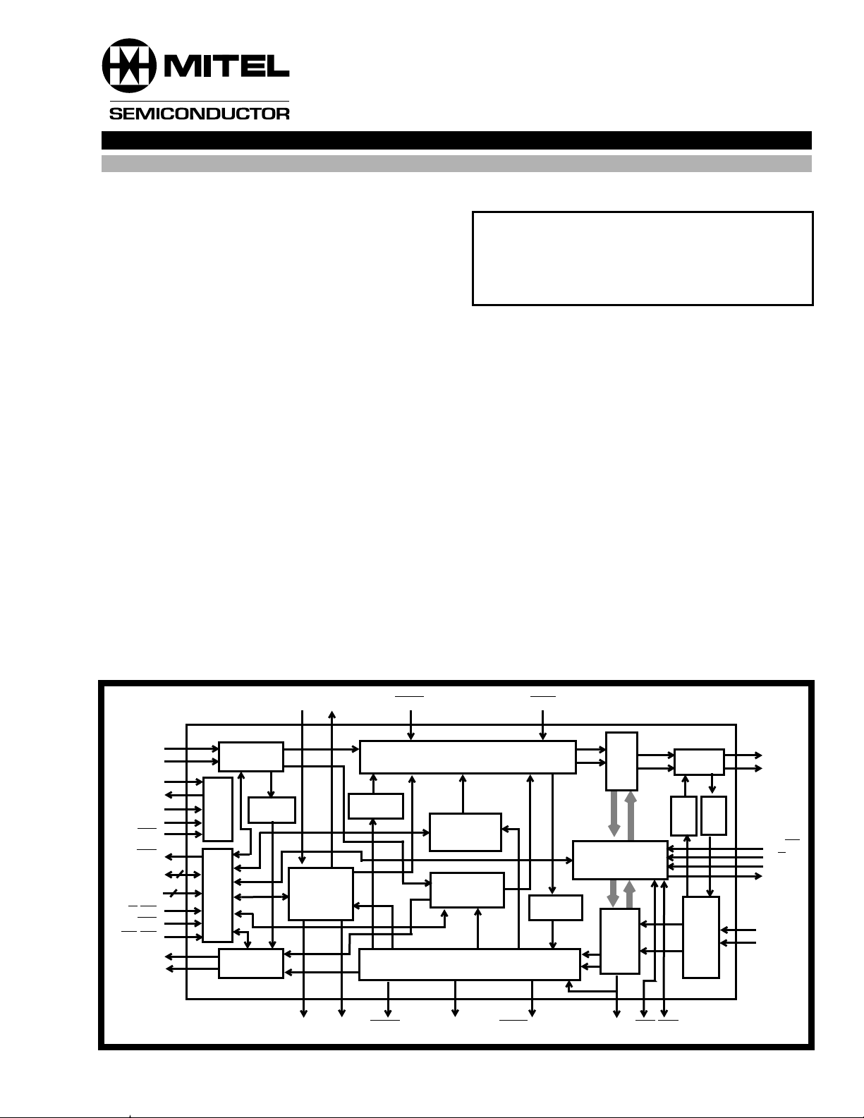
DSTi
CSTi
Tdi
Tdo
Tms
Tclk
Trst
IRQ
D7~D0
AC4
~AC0
R/W/WR
CS
DS/RD
DSTo
CSTo
ST-BUS
Interface
ST Loop
IEEE
1149.1
Interface
Microprocessor
ST-BUS
Interface
RxDLCLK RxDL
TxDL TxDLCLK
Data Link,
HDLC0,
HDLC1
Alarm Detection, 2 Frame Slip Buffer
TxMF
Transmit Framing, Error and
Test Signal Generation
PL Loop
National
Bit Buffer
CAS
Buffer
Receive Framing, Performance Monitoring,
Figure 1 - Functional Block Diagram
TAIS
DG Loop
RxFP/Rx64kCK
Pulse
Generator
Jitter Attenuator
& Clock Control
Recovery
Clock,Data
E2o
F0b C4bRxMF LOS
Line
Driver
RM
Loop
MT
Rx Equalizer
& Data Slicer
Loop
TTIP
TRING
MS/FR
M/S
OSC1
OSC2
RTIP
RRING
4-129
Page 2
MT9075A Preliminary Information
RESET
INT/
R/
W/WR
CS
IRQ
VSS
MOT
VDD
AC0
DSTi
CSTi
DS/RD
987654321
10
11
12
D0
13
D1
14
D2
15
D3
16
17
18
IC
19
20
21
D4
22
D5
23
D6
24
D7
25
26
27
AC1
CSTo
DSTo
282930313233343536373839404142
AC2
AC3
AC4
GNDARx
VDD
RTIP
VSS
OSC2
RRING
VDDARx
FR
BL/
OSC1
VSS
VDD
TxDL
TxDLCKICIC
68676665646362
NC
NC
VSS
VDD
RxDCLK
RxDL
TxMF
LOS
61
60
59
58
57
56
55
54
53
52
51
50
49
48
47
46
45
44
43
LS
BS/
RxMF
TAIS
Trst
Tclk
Tms
Tdo
Tdi
GNDATx
TRING
TTIP
VDDATx
VDD
VSS
IC
RxFP/Rx64KCK
F0b
C4b
E2o
68 PIN PLCC
RESET
INT/
R/
NC
NC
CS
IRQ
D0
D1
D2
D3
VSS
IC
MOT
VDD
D4
D5
D6
D7
W/WR
AC0
NC
82
84
86
88
90
92
94
96
98
100
NC
NC
NC
NC
NC
NC
NC
VSS
OSC1
OSC2
VSS
VDD
CSTo
CSTi
DSTo
DSTi
DS/RD
NC
NCNCNC
AC3
AC4
AC2
AC1
RTIP
GNDARx
RRING
VDARx
VDD
VSS
NC
NC
NC
100 PIN MQFP (JEDEC MO-112)
NC
IC
TCDLCK
TXDL
BL/FRVDD
22 24 26 28 30
2018161412108642
IC
IC
RXDL
TxMF
RXDLCK
LOS
IC
RxMF
NC
BL/LS
NCNCNC
NC
525456586062646668707274767880
NCNCNC
NC
NC
50
48
46
44
42
40
38
36
34
32
NC
NC
NC
TAIS
Trst
Tclk
Tms
Tdo
Tdi
GNDATx
TRING
TTIP
VDDATx
VDD
VSS
IC
RxFP/Rx64KCK
F0b
C4b
E2o
NC
4-130
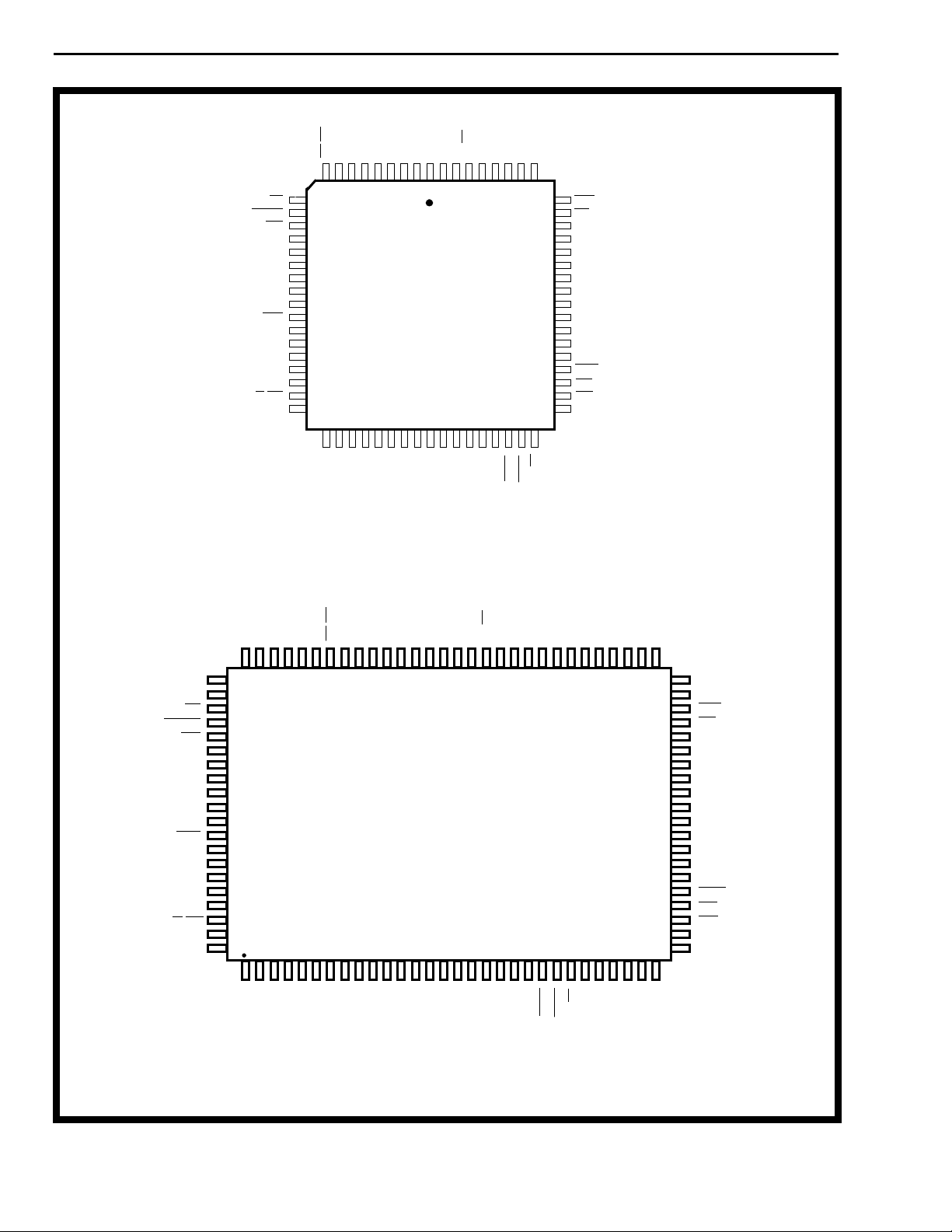
Figure 2 - Pin Connections
Page 3

Preliminary Information MT9075A
Pin Description
Pin #
Name Description
PLCC MQFP
1 66 OSC1 Oscillator Input. This pin is either connected via a 20.000 MHz crystal to OSC2 where a
crystal is used, or is directly driven when a 20.000 MHz oscillator is employed (see
Figures 6 and 7). Not suitable for TTL compatible oscillator.
2 67 OSC2 Oscillator Output. Not suitable for driving other devices. 368 VSSNegative Power Supply (Input). Digital ground. 469 VDDPositive Power Supply (Input). Digital supply (+5V ± 5%). 5 70 CSTo Control ST-BUS Output. CSTo carries one of the following two serial streams for CAS
and CCS respectively:
(i) A 2.048 Mbit/s ST-BUS status stream which contains the 30 receive signalling nibbles
(ABCDZZZZ or ZZZZABCD). The most significant nibbles of each ST-BUS time slot are
valid and the least significant nibbles of each ST-BUS time slot are tristated when control
bit MSN (page 01H, address 1AH, bit 1) is set to 1. If MSN=0, the position of the valid
and tristated nibbles is reversed.
(ii) A 64 kb/s output when the 64 KHz common channel signalling option is selected
(page 01H, address 1AH, bit 0, 64KCCS =1) for channel 16.
6 71 CSTi Control ST-BUS Input. CSTi carries one of the following two serial streams for CAS and
CCS respectively:
(i) A 2.048 Mbit/s ST-BUS control stream which contains the 30 transmit signalling
nibbles (ABCDXXXX or XXXXABCD) when page 01H, address 1AH, bit 3, RPSIG=0.
When RPSIG=1 this pin has no function. The most significant nibbles of each ST-BUS
time slot are valid and the least significant nibbles of each ST-BUS time slot are ignored
when control bit MSN (page 01H, address 1AH, bit 1) is set to 1. If MSN=0, the position
of the valid and ignored nibbles is reversed.
(ii) A 64 kb/s input when the 64 KHz common channel signalling option is selected (page
01H, address 1AH, bit 0, 64KCCS =1) for channel 16.
7 72 DSTo Data ST-BUS Output. A 2.048 Mbit/s serial stream which contains the 30 PCM or
data channels received on the PCM 30 line.
8 73 DSTi Data ST-BUS Input. A 2.048 Mbit/s serial stream which contains the 30 PCM or data
channels to be transmitted on the PCM 30 line.
974DS/RD Data/Read Strobe (Input).
In Motorola mode (DS), this input is the active low data strobe of the microprocessor
interface.
In Intel mode (RD), this input is the active low read strobe of the microprocessor
interface.
10 83 CS Chip Select (Input). This active low input enables the non-multiplexed parallel
microprocessor interface of the MT9075A. When CS is set to high, the
microprocessor interface is idle and all bus I/O pins will be in a high impedance state.
11 84 RESET RESET (Input). This active low input puts the MT9075A in a reset condition. RESET
should be set to high for normal operation. The MT9075A should be reset after powerup. The RESET pin must be held low for a minimum of 1µsec. to reset the device
properly.
12 85 IRQ Interrupt Request (Output). A low on this output pin indicates that an interrupt request
is presented. IRQ is an open drain output that should be connected to VDD through a
pull-up resistor. An active low CS signal is not required for this pin to function.
13 -1686-89D0 - D3 Data 0 to Data 3 (Three-state I/O). These signals combined with D4-D7 form the
bidirectional data bus of the microprocessor interface (D0 is the least significant bit).
4-131
Page 4

MT9075A Preliminary Information
Pin Description (continued)
Pin #
Name Description
PLCC MQFP
17 90 VSS Negative Power Supply (Input). Digital ground.
18 91 IC Internal Connection. Tie to VSS (Ground) for normal operation.
19 92 INT/MOT Intel/Motorola Mode Selection (Input). A high on this pin configures the processor
interface for the Intel parallel non-multiplexed bus type. A low configures the processor
interface for the Motorola parallel non-multiplexed type.
20 93 VDD Positive Power Supply (Input). Digital supply (+5V ± 5%).
21 -2494-97D4 - D7 Data 4 to Data 7 (Three-state I/O). These signals combined with D0-D3 form the
bidirectional data bus of the microprocessor interface (D7 is the most significant bit).
25 98 R/W/WR Read/Write/Write Strobe (Input).
In Motorola mode (R/W), this input controls the direction of the data bus D[0:7] during
a microprocessor access. When R/W is high, the parallel processor is reading data
from the MT9075A. When low, the microprocessor is writing data to the MT9075A.
For Intel mode (WR), this active low write strobe configures the data bus lines as
output.
26 -3099,
8-11
31 12 GNDARx Receive Analog Ground (Input). Analog ground for the LIU receiver.
323313
14
34 15 VDDARx Receive Analog Power Supply (Input). Analog supply for the LIU receiver (+5V ± 5%).
35 16 VDD Positive Power Supply (Input). Digital supply (+5V ± 5%).
36 17 VSS Negative Power Supply (Input). Digital ground.
37 18 IC Internal Connection. Must be left open for normal operation.
38 19 IC Internal Connection. Must be left open for normal operation.
39 20 RxDLCLK Receive Data Link Clock (Output). A gapped clock signal derived from a 2.048 Mbit/s
40 21 RxDL Receive Data Link (Output). A 2.048 Mbit/s data stream containing received line data
41 22 TxMF Transmit Multiframe Boundary (Input). An active low input used to set the transmit
42 23 RxMF Receive Multiframe Boundary (Output). An output pulse delimiting the received
AC0 -
AC4
RTIP
RRING
Address/Control 0 to 4 (Inputs). Address and control inputs for the microprocessor
interface. AC0 is the least significant input.
Receive TIP and RING (Inputs). Differential inputs for the receive line signal - must be
transformer coupled (See Figure 4).
clock, available for an external device to clock in RxDL data (at 4, 8, 12, 16 or 20 kHz) on
the rising edge.
after HDB3 decoding. This data is clocked out with the rising edge of E2o.
multiframe boundary (CAS or CRC multiframe). The MT9075A will generate its own
multiframe if this pin is held high. This input is usually pulled high for most applications.
multiframe boundary. The next frame output on the data stream (DSTo) is basic frame
zero on the PCM 30 link. This receive multiframe signal can be related to either the
receive CRC multiframe (page 01H, address 10H, bit 6, MFSEL=1) or the receive
signalling multiframe (MFSEL=0).
43 24 BS/LS System Bus Synchronous/Line Synchronous Selection (Input). If high, C4b and F0b
will be inputs; if low, C4b and F0b will be outputs.
44 32 E2o 2.048 MHz Extracted Clock (Output). The clock extracted from the received signal
and used internally to clock in data received on RTIP and RRING.
4-132
Page 5

Preliminary Information MT9075A
Pin Description (continued)
Pin #
Name Description
PLCC MQFP
45 33 C4b 4.096 MHz System Clock (Input/Output). C4b is the clock for the ST-BUS sections and
transmit serial PCM data of the MT9075A. In the free-run (BL/FR=0) or line synchronous
mode (BL/FR=1 and BS/LS=0) this signal is an output, while in the system bus
synchronous mode (BS/LS=1) this signal is an input clock.
46 34 F0b Frame Pulse (Input/Output). This is the ST-BUS or GCI frame synchronization
signal, which delimits the 32 channel frame of CSTi, CSTo, DSTi, DSTo and the
PCM30 link. In the free-run (BL/FR=0) or loop synchronous mode (BL/FR=1 and BS/
LS=0) this signal is an output, while in the Bus Synchronous mode (BL/FR=1 and BS/
LS=0) this signal is an input. The GCI/ST-BUS selection is made under software control.
Page 02H, address 13H, bit 0, GCI/ST=1 selects GCI frame pulse; GCI/ ST=0 selects STBUS.
47 35 RxFP/
Rx64KCK
Receive Frame Pulse/Receive CCS Clock (Output). An 8kHz pulse signal, which is
low for one extracted clock period. This signal is synchronized to the receive PCM 30
basic frame boundary.
When 64KCCS (page 01H, address 1AH, bit 0) is set to 1, this pin outputs a 64 kHz clock
derived by dividing down the e xtracted 2.048 MHz clock. This clock is used to clock CCS
data out of pin CSTo in the CCS mode.
48 36 IC Internal Connection. Must be left open for normal operation.
49 37 V
50 38 V
51 39 VDD
Negative Power Supply (Input). Digital ground.
SS
Positive Power Supply (Input). Digital supply (+5V ± 5%).
DD
Transmit Analog Power Supply (Input). Analog supply for the LIU transmitter (+5V ±
ATx
5%).
525340
41
54 42 GND
TTIP
TRING
ATx
Transmit TIP and RING (Outputs). Differential outputs for the transmit line signal - must
be transformer coupled (See Figure 4).
Transmit Analog Ground (Input). Analog ground for the LIU transmitter. 55 43 Tdi IEEE 1149.1 Test Data Input. If not used, this pin should be pulled high. 56 44 Tdo IEEE 1149.1 Test Data Output. If not used, this pin should be left unconnected. 57 45 Tms IEEE 1149.1 Test Mode Selection (Input). If not used, this pin should be pulled high. 58 46 Tclk IEEE 1149.1 Test Clock Signal (Input). If not used, this pin should be pulled high. 59 47 Trst IEEE 1149.1 Reset Signal (Input). If not used, this pin should be held low. 60 48 TAIS Transmit Alarm Indication Signal (Input). An active low on this input causes the
MT9075A to transmit an AIS (all ones signal) on TTIP and TRING pins. TAIS should be
set to high for normal data transmission.
61 57 LOS Loss of Signal or Synchronization (Output). When high, and LOS/LOF (page 02H
address 13H bit 2) is zero, this signal indicates that the receiv e portion of the MT9075A is
either not detecting an incoming signal (bit LLOS on page 03H address 18H is one) or is
detecting a loss of basic frame alignment condition (bit SYNC on page 03H address 10H
is one). If LOS/LOF=1, a high on this pin indicates a loss of signal condition.
62 58 IC Internal Connection. Tie to VSS (Ground) for normal operation.
59 NC No Connection. Leave open for normal operation.
63 60 IC Internal Connection. Tie to VSS (Ground) for normal operation.
4-133
Page 6

MT9075A Preliminary Information
Pin Description (continued)
Pin #
Name Description
PLCC MQFP
64 61 TxDLCLK Transmit Data Link Clock (Output). A gapped clock signal derived from a gated 2.048
Mbit/s clock for transmit data link at 4, 8, 12, 16 or 20 kHz. The transmit data link data
(TxDL) is clocked in on the rising edge of TxDLCLK. TxDLCLK can also be used to clock
DL data out of an external serial controller.
65 62 TxDL Transmit Data Link (Input). An input serial stream of transmit data link data at 4, 8, 12,
16 or 20 kbit/s composed of 488ns-wide bit cells which are multiplexed into selected
national bits of the PCM 30 transmit signal.
66 63 BL/FR BusorLine/Freerun (Input). If this pin is set to high, the MT9075A is in the System Bus
or Line Synchronous mode depending on the BS/LS pin. If low, the MT9075A is in the
free run mode.
67 64 VDD Positive Power Supply (Input). Digital supply (+5V ± 5%).
68 65 VSS Negative Power Supply (Input). Digital ground.
1-7,
25-31,
49-56,
75-82,
100
NC No Connection. Leave open for normal operation.
4-134
Page 7

Preliminary Information MT9075A
Device Overview
The MT9075A is an advanced PCM 30 framer with
an on-chip Line Interface Unit (LIU) that meets or
supports the latest ITU-T Recommendations for
PCM 30 and ISDN primary rate including G.703,
G.704, G.706, G.775, G.796, G.732, G.823 and
I.431. It also meets or supports the layer 1
requirements of ETSI ETS 300 166 and BS6450.
The Line Interface Unit (LIU) of the MT9075A
interfaces the digital framer functions to the PCM 30
transformer-isolated four wire line. The transmit
portion of the MT9075A LIU consists of a digital
buffer, a digital-to-analog converter and a differential
line driver. The receiver portion of the LIU consists of
an input signal peak detector, an optional two-stage
equalizer, a smoothing filter, data and clock slicers
and a clock extractor. The optional equalizer allows
for error free reception of data with a line attenuation
of up to 20 dB.
The LIU also contains a Jitter Attenuator (JA), which
can be configured to either the transmit or receive
path. The JA will attenuate jitter from 2.5 Hz and roll-
off at a rate of 20 dB/decade. Its intrinsic jitter is less
than 0.02 UI.
The digital portion of the MT9075A connects an
incoming stream of time multiplexed PCM channels
(at 2.048 Mbit/s) to the transmit payload of the E1
trunk, while the receive payload is connected to the
ST-BUS or GCI 2.048 Mbit/s backplane bus for both
data and signalling. Control, reporting and
conditioning of the line is implemented via a parallel
microprocessor interface. The MT9075A framing
algorithm allows automatic interworking between
CRC-4 and non-CRC-4 interfaces.
The Sa bits can be accessed by the MT9075A in the
following four ways:
data link maintenance channel to be modified and
updates the CRC-4 remainder bits to reflect the
modification. All channel, framing and signalling data
passes through the device unaltered. This is useful
for intermediate point applications of a PCM 30 link
where the data link data is modified, but the error
information transported by the CRC-4 bits must be
passed to the terminating end. In the receive
transparent mode, the received line data is
channelled to DSTo with framing operations
disabled, consequently, the data passes through the
slip buffer and drives DSTo with an arbitrary
alignment.
The MT9075A has a comprehensive suite of status,
alarm, performance monitoring and reporting
features. These include counters for BPVs, CRC
errors, E-bit errors, errored frame alignment signals,
BERT, and RAI and continuous CRC errors. Also,
included are transmission error insertion for BPVs,
CRC-4 errors, frame and non-frame alignment signal
errors, payload errors and loss of signal errors.
A complete set of loopback functions is provided,
which includes digital, remote, ST-BUS, payload,
metallic, local and remote time slot.
The MT9075A also contains a comprehensive set of
maskable interrupts and an interrupt vector function.
Interrupt sources consist of synchronization status,
alarm status, counter indication and overflow, timer
status, slip indication, maintenance functions and
receive channel associated signalling bit changes. A
special set of maskable interrupts have been
included for sensing changes in the state of the
national use bits and nibbles, in compliance to
emerging ETS requirements.
The MT9075A system timing may be slaved to the
line, operated in freerun mode, or controlled by an
external timing source.
• Single byte registers;
• Five byte transmit and receive national bit
buffers;
• Data link pins TxDL, RxDL, RxDLCLK and
TxDLCLK;
• HDLC Controller with a 128 byte FIFO.
The MT9075A operates in either termination or
transparent modes selectable via software control. In
the termination mode the CRC-4 calculation is
performed as part of the framing algorithm. In the
transmit transparent mode, no framing or signalling
is imposed on the data transmit from DSTi on the
line. In addition, the MT9075A optionally allows the
4-135
Page 8

MT9075A Preliminary Information
Functional Description
MT9075A Line Interface Unit (LIU)
Receiver
The receiver portion of the MT9075A LIU consists of
an input signal peak detector, an optional two-stage
equalizer, a smoothing filter, adaptive threshold
comparators, data and clock slicers, and a clock
extractor. Receive equalization gain can be set via
software control or it can be determined
automatically by the peak detectors.
The output of the receive equalizer is conditioned by
a smoothing filter and is passed on to the clock and
data slicer. The clock slicer output signal drives a
phase locked loop, which generates the extracted
clock (E2o). This extracted clock is used to sample
the output of the data comparator.
The LOS output pin (pin 61 in PLCC, pin 57 in
MQFP) is user selectable, by setting control bit LOS/
LOF (page 02H, register 13H, bit 2), to indicate a
loss of signal or loss of basic frame synchronization
condition. In addition, a status bit, LLOS (bit 4 in
page 3, register 18H) is provided to indicate the
presence of a loss signal condition. The occurrence
of a loss signal condition is defined as per I.431, i.e.,
when the incoming signal amplitude is more than 20
dB below the nominal amplitude for a time duration
of at least 1 ms.
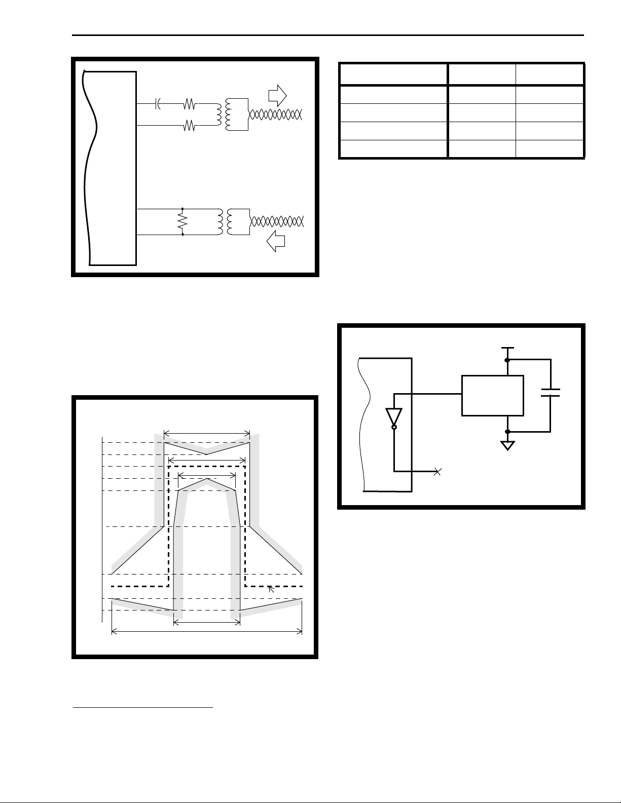
The receive LIU circuit requires a terminating
resistor of either 120Ω or 75Ω across the device side
of the receive1:1 transformer as shown in Figure 4.
The return loss of the receiver, complying with
G.703, is greater than:
• 12 dB from 51 kHz to 102 kHz;
• 18 dB from 102 kHz to 2048 kHz;
• 14 dB from 2048 kHz to 3072 kHz.
The jitter tolerance of the MT9075A clock extractor
circuit exceeds the requirements of G.823 (Figure 3).
Transmitter
The MT9075A differential line driver is designed to
drive a 1:2 step-up transformer (see Figure 4). In
120 Ω twisted pair applications, a 0.68 uF capacitor is
required between the TTIP and the transmit
transformer. For 75 Ω coaxial cable applications, a
0.68 uF capacitor and two 2.2 Ω series resistors are
required between the transformer and the TTIP and
TRING output pins as shown in Figure 4.
4-136
Peak to Peak
Jitter Amplitude
(log scale)
18UI
MT9075A
Tolerance
1.5UI
0.2UI
Jitter Frequency
(log scale)
1.667Hz 20Hz 2.4kHz 18kHz 100kHz
Figure 3 - Typical Jitter Tolerance
Page 9
Preliminary Information MT9075A
Tx
TTIP
TRING
MT9075A
RTIP
RRING
0.68uF
2.4Ω*
2.4Ω*
1:2
* 2.4 Ω resistors are only
required with 75 Ωcoax
1:1
120Ω/
75Ω
Rx
Figure 4 - Analog Line Interface
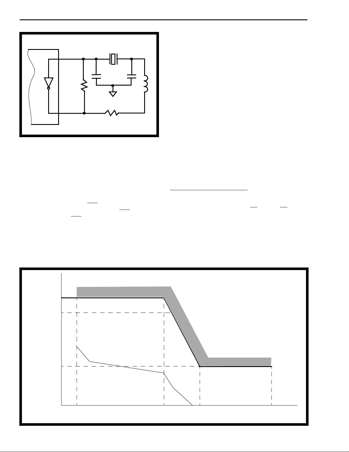
The template for the transmitted pulse, as specified in
G703, is shown in Figure 5. The nominal peak voltage
of a mark is 3 volts for 120 Ω twisted pair applications
and 2.37 volts for 75 Ω coax applications. The ratio of
the amplitude of the transmit pulses generated by TTP
and TRING is between 0.95 and 1.05.
Percentage of
Nominal Peak
120
110
100
90
80
269nS
244nS
194nS
Manufacturer For Tx For Rx
Filtran 5721-1 5721-2
Pulse Engineering PE-65351 PE-64934
Midcom 50027 50026
OSEC 02934/A 02935/A
Table 1 - Transformer Manufacturers and Part
Numbers
Timing Source
The MT9075A can use either a clock or crystal,
connecting to pins OSC1 and OSC2, as the
reference timing source.
Figure 6 shows a 20MHz clock oscillator, with 50ppm
tolerance, directly connected to the OSC1 pin of the
MT9075A.
+5V
MT9075A
OSC1
OSC2
20MHz
OUT
Vdd
GND
.1µF
(open)
50
10
0
-10
-20
219nS
488nS
Nominal Pulse
Figure 5 - Pulse Template (G.703)
Transformer Recommendation
Table 1 shows a list of recommended transformers
for the MT9075A line interface.
Figure 6 - Clock Oscillator Circuit
Alternatively, a crystal oscillator may be used. A
complete oscillator circuit made up of a crystal,
resistors and capacitors is shown in Figure 7. The
crystal specification is as follows.
Frequency: 20MHz
Tolerance: 50ppm
Oscillation Mode: Fundamental
Resonance Mode: Parallel
Load Capacitance: 32pF
Maximum Series Resistance: 35
Ω
Approximate Drive Level: 1mW
4-137
Page 10
MT9075A Preliminary Information
jittered clock is used to clock the data out of the
FIFO.
MT9075A
OSC1
1MΩ
OSC2
Note: the 1µH inductor is optional
Figure 7 - Crystal Oscillator Circuit
56pF
20MHz
100Ω
39pF
1µH*
The JA meets the jitter transfer characteristics as
proposed by G.823 and the relevant
recommendations as shown in Figure 8. The JA
FIFO depth can be selected to be from 16 to 128
words deep, in multiples of 16 (2-bit) words. Its read
pointer can be centered by changing the JFC bit
(address 18H of page 02H) to provide maximum jitter
tolerance. If the read pointer should come within 4
bits of either end of the FIFO, the read clock
frequency will be increased or decreased by 0.0625
UI to correct the situation. The maximum time
needed to centre is T
= 3904∗Depth ns, where
max
Depth is the selected JA FIFO depth. During this
time the JA will not attenuate jitter.
Jitter Attenuator (JA)
The MT9075A Jitter Attenuator (JA), which consists
of a Phase Locked Loop (PLL) and data FIFO, can
be used on either the transmit or receive side of the
interface.
On the transmit side the C4b signal clocks the data
into the FIFO, the PLL de-jitters the C4b clock and
the resulting clean C4b signal clocks the data out of
the FIFO.
When the JA is selected on the receive side, the
extracted clock signal clocks the data into the FIFO.
The same clock feeds the PLL and the resulting de-
dB
0.5
0
To ensure normal operation, the JA FIFO depth
should be set in software to be larger than the
anticipated maximum UI of input jitter.
Clock Jitter Attenuation Modes
MT9075A has three basic jitter attenuation modes of
operation, selected by the BS/LS and BL/FR control
pins.
• System Bus Synchronous Mode.
• Line Synchronous Mode.
• Free-run mode.
4-138
-20 dB/decade
JITTER ATTENUATION (dB)
-19.5
10 40 400 10K
Frequency (Hz)
Figure 8 - Typical Jitter Attenuation Curve
Page 11

Preliminary Information MT9075A
Mode Name BS/LS BL/FR JAS JAT/JAR Note
SysBusSync1 1 1 1 1 JA on Tx side; No JA on Rx side
SysBusSync2 1 1 1 0 JA on Rx side; No JA on Tx side
SysBusSync3 1 1 0 x No JA on Tx or Rx side
Line
Synchronous
Free-Run x 0 x x In free-run mode JA will be automatically
Depending on the mode selected, the Jitter
Attenuator (JA) can attenuate either transmit clock
jitter or receive clock jitter, or be disconnected.
Control bits JAS, JAT/JAR (address 18H of page
02H) determine the JA selection under certain
modes. Table 2 shows the configuration of related
control pins and control bits required to place the
MT9075A in the appropriate jitter attenuation mode.
Referring to the mode names given in Table 2, the
basic operation of the jitter attenuation modes is
summarized as follows:
•In
•In
•In
•In
•In
SysBusSync
F0b are always configured as inputs, while in
the Line Synchronous and Free-Run modes
C4b and F0b are configured as outputs.
SysBusSync1
applied to C4b. The applied clock is
dejittered by the internal PLL before being
used to transmit data. The clock extracted
(with no jitter attenuation performed) from
the receive data can be monitored on pin
E2o.
SysBusSync2
pin C4b is assumed to be jitter-free and is
directly used to transmit data. The internal
PLL is used to dejitter the extracted receive
clock. The dejittered receive clock is output
on pin E2o.
SysBusSync3
is applied to either the transmit or receive
clocks. The transmit data is synchronized to
clock applied to pin C4b. The extracted
receive clock is not dejittered and is supplied
directly to the E2o output.
Line Synchronous
extracted from the receive data is dejittered
using the internal PLL and then output on pin
C4b. Pin E2o provides the extracted receive
0 1 x x By default, JA is on the receive side.
Controls bits need not be selected.
disconnected
Table 2 - Selection of Clock Jitter Attenuation Modes
clock before it has been dejittered. The
transmit data is synchronous to the clean
receive clock.
(1-3) modes, pins C4b and
mode, an external clock is
mode, the clock applied to
mode, no jitter attenuation
mode, the clock
•In
The PCM 30 Interface
PCM 30 (E1) basic frames are 256 bits long and are
transmitted at a frame repetition rate of 8000 Hz,
which results in an aggregate bit rate of 256 bits x
8000/sec = 2.048 Mbits/sec. The actual bit rate is
2.048 Mbits/sec +/-50 ppm encoded in HDB3 format.
The HDB3 control bit (page 01H, address 15H, bit 5)
selects either HDB3 encoding or alternate mark
inversion (AMI) encoding. Basic frames are divided
into 32 time slots numbered 0 to 31, see Figure 31.
Each time slot is 8 bits in length and is transmitted
most significant bit first (numbered bit 1). This results
in a single time slot data rate of 8 bits x 8000/sec. =
64 kbits/sec.
It should be noted that the Mitel ST-BUS also has 32
channels numbered 0 to 31, but the most significant
bit of an eight bit channel is numbered bit 7 (see
Mitel Application Note MSAN-126). Therefore, STBUS bit 7 is synonymous with PCM 30 bit 1; bit 6
with bit 2: and so on (Figure 31).
PCM 30 time slot 0 is reserved for basic frame
alignment, CRC-4 multiframe alignment and the
communication of maintenance information. In most
configurations time slot 16 is reserved for either
Channel Associated Signalling (CAS or ABCD bit
signalling) or Common Channel Signalling (CCS).
The remaining 30 time slots are called channels and
carry either PCM encoded voice signals or digital
Free-Run
synchronized to the internally generated
clock. The internal clock is output on pin
C4b. The clock signal extracted from the
receive data is not dejittered and is output
directly on pin E2o.
mode the transmit data is
4-139
Page 12

MT9075A Preliminary Information
data. Channel alignment and bit numbering is
consistent with time slot alignment and bit
numbering. However, channels are numbered 1 to 30
and relate to time slots as per Table 3.
PCM 30
Timeslot
Voice/Data
Channels
Table 3 - Time Slot to Channel Relationship
Basic Frame Alignment
Time slot 0 of every basic frame is reserved for basic
frame alignment and contains either a Frame
Alignment Signal (FAS) or a Non-Frame Alignment
Signal (NFAS). FAS and NFAS occur in time slot zero
of consecutive basic frames as shown in Table 7. Bit
two is used to distinguish between FAS (bit two = 0)
and NFAS (bit two = 1).
Basic frame alignment is initiated by a search for the
bit sequence 0011011 which appears in the last
seven bit positions of the FAS, see the Frame
Algorithm section. Bit position one of the FAS can be
either a CRC-4 remainder bit or an international
usage bit.
0 1 2 3...15 16 17 18 19...31
x 1 2 3...15 x 16 17 18...30
CRC-4 Multiframing
The primary purpose for CRC-4 multiframing is to
provide a verification of the current basic frame
alignment, although it can also be used for other
functions such as bit error rate estimation. The CRC4 multiframe consists of 16 basic frames numbered 0
to 15, and has a repetition rate of 16 frames X 125
microseconds/frame = 2 msec.
CRC-4 multiframe alignment is based on the 001011
bit sequence, which appears in bit position one of the
first six NFASs of a CRC-4 multiframe.
The CRC-4 multiframe is divided into two
submultiframes, numbered 1 and 2, which are each
eight basic frames or 2048 bits in length.
The CRC-4 frame alignment verification functions as
follows. Initially, the CRC-4 operation must be
activated and CRC-4 multiframe alignment must be
achieved at both ends of the link. At the local end of
a link, all the bits of every transmit submultiframe are
passed through a CRC-4 polynomial (multiplied by
X4 then divided by X4 + X + 1), which generates a
four bit remainder. This remainder is inserted in bit
position one of the four FASs of the following
submultiframe before it is transmitted (see Table 7).
Bits four to eight of the NFAS (i.e., Sa4 - Sa8) are
additional spare bits which may be used as follows:
•Sa4 to Sa8 may be used in specific point-to-point
applications (e.g. transcoder equipments
conforming to G.761).
•Sa4 may be used as a message-based data link
for operations, maintenance and performance
monitoring.
•Sa5to Sa8 are for national usage.
A maintenance channel or data link at 4,8,12,16,or
20 kHz for selected Sa bits is provided by the
MT9075A to implement these functions. Note that for
simplicity all Sa bits including Sa4 are collectively
called national bits throughout this document.
Bit three (designated as “A”), the Remote Alarm
Indication (RAI), is used to indicate the near end
basic frame synchronization status to the far end of a
link. Under normal operation, the A (RAI) bit should
be set to 0, while in alarm condition, it is set to 1.
Bit position one of the NFAS can be either a CRC-4
multiframe alignment signal, an E-bit or an
international usage bit. Refer to an approvals
laboratory and national standards bodies for specific
requirements.
The submultiframe is then transmitted and, at the far
end, the same process occurs. That is, a CRC-4
remainder is generated for each received
submultiframe. These bits are compared with the bits
received in position one of the four FASs of the next
received submultiframe. This process takes place in
both directions of transmission.
When more than 914 CRC-4 errors (out of a possible
1000) are counted in a one second interval, the
framing algorithm will force a search for a new basic
frame alignment. See Frame Algorithm section for
more details.
The result of the comparison of the received CRC-4
remainder with the locally generated remainder will
be transported to the far end by the E-bits.
Therefore, if E1 = 0, a CRC-4 error was discovered in
a submultiframe 1 received at the far end; and if E2 =
0, a CRC-4 error was discovered in a submultiframe
2 received at the far end. No submultiframe
sequence numbers or re-transmission capabilities
are supported with layer 1 PCM 30 protocol. See
ITU-T G.704 and G.706 for more details on the
operation of CRC-4 and E-bits.
4-140
Page 13
Preliminary Information MT9075A
SYNC CRCSYN CRCIWK Recommended Transmit RAI setting
0 0 1 Set transmit RAI continuously low.
0 0 0 This state cannot exist with AUTC set low.
1 1 x Set transmit RAI continuously high.
0 1 1 Transmit a flickering (0 to 1 to 0) RAI every 8 milliseconds.
0 1 0 The link is a CRC to non CRC link. Set transmit RAI to the appropriate
stable state (usually low).
Table 4 - Transmit RAI setting for CRC to non CRC interworking with AUTC set low
There are two CRC multiframe alignment algorithm
options selected by the AUTC control bit (address
11H, page 01H). When AUTC is zero and CSYN is
zero, automatic CRC-to-non-CRC interworking is
selected, if CRC-4 multiframe alignment is not found
in 400 msec, the status bit CRCIWK (page 03H,
address 10H) is set low and no further attempt to
achieve CRC-4 synchronization is made as long as
the device remains in terminal frame
synchronization. When AUTC is one and CSYN is
zero, a reframe will be initiated every 8 msec if the
MT9075A achieves terminal frame synchronization,
but fails to achieve CRC-4 synchronization.
The control bit for transmit E bits (TE, bit 4 at
address 16H of page 01H) will have the same
function in both states of AUTC. That is, when CRC-4
synchronization is not achieved the state of the
transmit E-bits will be the same as the state of the TE
control bit. When CRC-4 synchronization is achieved
the transmit E-bits will function as per ITU-T G.704.
Table 4 outlines the recommended setting of the
TALM control bits of the MT9075A.
which occurs in the most significant nibble of time
slot 16 of basic frame 0 of the CAS multiframe. Bit 6
of this time slot is the multiframe alarm bit (usually
designated Y). When CAS multiframing is acquired
on the receive side, the transmit Y-bit is zero; when
CAS multiframing is not acquired, the transmit Y-bit is
one. Bits 5, 7 and 8 (usually designated X) are spare
bits and are normally set to one if not used.
Time slot 16 of the remaining 15 basic frames of the
CAS multiframe (i.e., basic frames 1 to 15) are
reserved for the ABCD signalling bits for the 30
payload channels. The most significant nibbles are
reserved for channels 1 to 15 and the least
significant nibbles are reserved for channels 16 to
30. That is, time slot 16 of basic frame 1 has ABCD
for channel 1 and 16, time slot 16 of basic frame 2
has ABCD for channel 2 and 17, through to time slot
16 of basic frame 15 has ABCD for channel 15 and
30.
MT9075A Access and Control
CAS Signalling Multiframing
The purpose of the signalling multiframing algorithm
is to provide a scheme that will allow the association
of a specific ABCD signalling nibble with the
appropriate PCM 30 channel. Time slot 16 is
reserved for the communication of Channel
Associated Signalling (CAS) information (i.e., ABCD
signalling bits for up to 30 channels). Refer to ITU-T
G.704 and G.732 for more details on CAS
multiframing requirements.
A CAS signalling multiframe consists of 16 basic
frames (numbered 0 to 15), which results in a
multiframe repetition rate of 2 msec. It should be
noted that the boundaries of the signalling multiframe
may be completely distinct from those of the CRC-4
multiframe. CAS multiframe alignment is based on a
multiframe alignment signal (a 0000 bit sequence),
Register Access
The control and status of the MT9075A is achieved
through a non-multiplexed parallel microprocessor
port. The parallel port may be configured for
Motorola style control signals (by setting pin INT/
MOT low) or Intel style control signals (by setting pin
INT/MOT high).
The controlling microprocessor gains access to
specific registers of the MT9075A through a two step
process. First, writing to the internal Command/
Address Register (CAR) selects one of the 18 pages
of control and status registers (CAR address: AC4 =
0, AC3-AC0 = don't care, CAR data D7 - D0 = page
number). Second, each page has a maximum of 16
registers that are addressed on a read or write to a
non-CAR address (non-CAR: address AC4 = 1, AC3AC0 = register address, D7-D0 = data). Once a page
4-141
Page 14

MT9075A Preliminary Information
of memory is selected, it is only necessary to write to
the CAR when a different page is to be accessed.
See Figures 11 and 12 for timing requirements.
Please note that for microprocessors with read/write
cycles less than 200 ns, a wait state or a dummy
operation (for C programming) between two
successive read/write operations to the HDLC FIFO
is required.
Table 5 associates the MT9075A control and status
pages with access and page descriptions.
ST-BUS Streams
The ST-BUS stream can also be used to access
channel associated signalling nibbles. CSTo contains
the received channel associated signalling bits (e.g.,
ITU-T R1 and R2 signalling), and when control bit
RPSIG (page 01H, address 1AH) is set to 0, CSTi is
used to control the transmit channel associated
signalling. The DSTi and DSTo streams contain the
transmit and receive voice and digital data.
Identification Code
The MT9075A shall be identified by the code
10101010, read from the identification code status
register (page 03H, address 1FH).
Reset Operation (Initialization)
The MT9075A can be reset using the hardware
RESET pin (pin 11 in PLCC, pin 84 in MQFP, see pin
description for external reset circuit requirements) or
the software reset bit RST (page 01H, address 11H).
When the device emerges from its reset state it will
begin to function with the default settings described
in Table 6. A reset operation takes 1 full frame (125
us) to complete.
Page Address
D7 - D
0
00000001 (01H) Master
00000010 (02H) R/W
00000011 (03H) Master
00000100 (04H) R/W
00000101 (05H) Per Channel Transmit Signalling R/W CSTi
00000110 (06H) Per Channel Receive Signalling R CSTo
00000111 (07H) Per Time Slot
00001000 (08H) R/W
00001001 (09H) 1 Second Status R --00001010 (0AH) unused --00001011 (0BH) HDLC0 Control and Status (TS 0) R/W --00001100 (0CH) HDLC1 Control and Status (TS 16) R/W --00001101 (0DH) Transmit National Bit Buffer R/W --00001110 (0EH) Receive National Bit Buffer R --00001111 (0FH) Tx message mode Buffer 0 R/W --00010000 (10H) Tx message mode Buffer 1 R/W --00010001 (11H) Rx message mode Buffer 0 R/W --00010010 (12H) Rx message mode Buffer 1 R/W ---
Control
Status
Control
Register Description
Table 5 - Register Summary
Processor
Access
R/W
R
R/W
ST-BUS
Access
--
---
---
4-142
Page 15
Preliminary Information MT9075A
a
Function Status
Mode Termination
Loopbacks Deactivated
Transmit FAS Cn0011011
Transmit non-FAS 1/Sn1111111
Transmit MFAS (CAS) 00001111
Data Link Deactivated
CRC Interworking Activated
Signalling CAS Registers
ABCD Bit Debounce Deactivated
Interrupts Interrupt Mask Word
Zero unmasked, all
others masked;
interrupts not suspended
RxMF Output Signalling Multiframe
Error Insertion Deactivated
HDLCs Deactivated
Counters Cleared
Tx Message Buffer All locations set to 54H
Per Time Slot Control
All locations cleared
Buffer
Table 6 - Reset Status
Transmit AIS Operation
CRC
CRC
Frame/
Type
0/FAS C10011011
1/NFAS
2/FAS C20011011
3/NFAS
4/FAS C30011011
5/NFAS
Sub Multi Frame 1
6/FAS C40011011
7/NFAS
8/FAS C10011011
9/NFAS
10/FAS C20011011
11/NFAS
12/FAS C30011011
13/NFAS E
Sub Multi Frame 2
14/FAS C40011011
15/NFAS E
PCM 30 Channel Zero
12345678
01ASa4Sa5Sa6Sa7S
01ASa4Sa5Sa6Sa7S
11ASa4Sa5Sa6Sa7S
01ASa4Sa5Sa6Sa7S
11ASa4Sa5Sa6Sa7S
11ASa4Sa5Sa6Sa7S
1ASa4Sa5Sa6Sa7S
1
1ASa4Sa5Sa6Sa7S
2
Table 7 - FAS and NFAS Structure
a8
a8
a8
a8
a8
a8
a8
a8
The pin TAIS (Tr ansmit AIS, pin 60 in PLCC, pin 48 in
MQFP) allows an all ones signal to be transmitted
from the point of power-up without the need to write
any control registers. During this time the IRQ pin is
tristated. After the interface has been initialized
normal operation can take place by making TAIS
high.
National Bit Buffers
Table 7 shows the contents of the transmit and
receive Frame Alignment Signals (FAS) and Nonframe Alignment Signals (NFAS) of time slot zero of
a PCM 30 signal. Even numbered frames (CRC
Frame # 0, 2, 4,...) are FASs and odd numbered
frames (CRC Frame # 1, 3, 5,...) are NFASs. The bits
of each channel are numbered 1 to 8, with bit 1 being
the most significant and bit 8 the least significant.
indicates position of CRC-4 multiframe alignment sign
Table 8 illustrates the organization of the MT9075A
transmit and receive national bit buffers. Each row is
an addressable byte of the MT9075A national bit
buffer, and each column contains the national bits of
an odd numbered frame of each CRC-4 Multiframe.
The transmit and receive national bit buffers are
located at page 0DH and 0EH respectively.
Addre
ssable
Bytes
NBB0 S
NBB1 S
NBB2 S
NBB3 S
NBB4 S
Frames 1, 3, 5, 7, 9, 11, 13 & 15 of a CRC-4
Multiframe
F1 F3 F5 F7 F9 F11 F13 F15
a4Sa4Sa4Sa4Sa4Sa4Sa4Sa4
a5Sa5Sa5Sa5Sa5Sa5Sa5Sa5
a6Sa6Sa6Sa6Sa6Sa6Sa6Sa6
a7Sa7Sa7Sa7Sa7Sa7Sa7Sa7
a8Sa8Sa8Sa8Sa8Sa8Sa8Sa8
Table 8 - MT9075A National Bit Buffers
Note that the Data Link (DL) pin functions, if
selected, override the transmit national bit buffer
function.
4-143
Page 16

MT9075A Preliminary Information
The CRC-4 Alignment status CALN (page 03H,
address 12H) and maskable interrupt CALNI (page
01H, address 1DH) indicate the beginning of every
received CRC-4 multiframe.
Maskable interrupts are available for change of state
of Sa5 bits or change of state of Sa6 nibbles. By
writing the proper control bits, an interrupt can be
generated on a change of state of any Sa bit (except
Sa4 - normally reserved for the data link), or any
nibbles for Sa5 through Sa8. See the description of
page 01H, address 19H for more details.
In addition, the transparent transmission of channel
0 is supported to meet the ETS requirement.
Selectable on a bit by bit basis, Sa bits in channel 0
DSTi data can be programmed using register 17H of
page 01H to be sent transparently onto the line.
Data Link Operation
Timeslot 0
The MT9075A has a user defined 4, 8, 12, 16 or 20
kbit/s data link for transport of maintenance and
performance monitoring information across the PCM
30 link. This channel functions using the Sa bits
(Sa4~Sa8) of the PCM 30 timeslot zero non-frame
alignment signal (NFAS). Since the NFAS is
transmitted every other frame - a periodicity of 250
microseconds - the aggregate bit rate is a multiple of
4 kb/s. As there are five Sa bits independently
available for this data link, the bit rate will be 4, 8, 12,
16 or 20 kb/s, depending on the bits selected for the
Data Link (DL).
The RxDLCLK signal (pin 39 in PLCC, pin 20 in
MQFP) is derived from the receive extracted clock
and is aligned with the receive data link output RxDL.
The HDB3 decoded receive data, at 2.048 Mbit/s, is
clocked out of the device on pin RxDL (pin 40 in
PLCC, pin 21 in MQFP). In order to facilitate the
attachment of this data stream to a Data Link
controller, the clock signal RxDLCLK consists of
positive pulses, of nominal width of 244 ns, during
the Sa bit cell times that are selected for the data
link. Again, this selection is made by programming
address 10H of master control page 01H. No DL
data will be lost or repeated when a receive frame
slip occurs. See Figures 13-16 for timing
requirements.
Timeslot 16
Channel 16 may be used to create a transparent 64
kb/s clear channel. In this event CSTi (pin 6 in PLCC,
pin 71 in MQFP) becomes the data input pin for
channel 16 transmit data, and CSTo (pin 5 in PLCC,
pin 70 in MQFP) becomes a 64 kb/s serial output
link. The CSTo output link is synchronous to the
extracted clock timebase. The pin Rx64KCK (pin 47
in PLCC, pin 35 in MQFP) provides a 64 kHz clock
for use with 64 kb/s data emanating from CSTo. The
64 kb/s input data from CSTi is clocked in with an
internal 64 kHz clock synchronous to the I/O pin C4b
(pin 45 in PLCC, pin 33 in MQFP) timebase. The
internal clock toggles coincident with every second
ST-BUS channel boundar y, with the first r ising edge
of a frame occurring at the beginning of ST-BUS
channel 2.
Dual HDLC
The Sa bits used for the DL are selected by setting
the appropriate bits, Sa4~Sa8, to one in the Data Link
Select Word (page 01H, address 10H, bits 4-0).
Access to the DL is provided by pins TxDLCLK,
TxDL, RxDLCLK and RxDL, which allow easy
interfacing to an external controller.
Data to be transmit onto the line in the Sa bit position
is clocked in from the TxDL pad (pin 65 in PLCC, pin
62 in MQFP) with the clock TxDLCLK (pin 64 in
PLCC, pin 61 in MQFP). Although the aggregate
clock rate equals the bit rate, it has a nominal pulse
width of 244 ns, and it clocks in the TxDL as if it were
a 2.048 Mb/s data stream. The clock can only be
active during bit times 4 to 0 of the STBUS frame.
The TxDL input signal is clocked into the MT9075A
by the rising edge of TxDLCLK. If bits are selected to
be a part of the DL, all other programmed functions
for those Sa bit positions are overridden.
4-144
The MT9075A has two identical HDLC controllers
(HDLC0, HDLC1) for the Sa bits and channel 16
respectively. The following features are common to
both HDLC controllers:
• Independent transmit and receive FIFO's;
• Receive FIFO maskable interrupts for nearly
full (programmable interrupt levels) and
overflow conditions;
• Transmit FIFO maskable interrupts for
nearly empty (programmable interrupt
levels) and underflow conditions;
• Maskable interrupts for transmit end-ofpacket and receive end-of-packet;
• Maskable interrupts for receive bad-frame
(includes frame abort);
• Transmit end-of-packet and frame-abort
functions.
Page 17

Preliminary Information MT9075A
HDLC0 Functions
When connected to the Data Link (DL) HDLC0 will
operate at a selected bit rate of 4, 8, 12, 16 or 20
kbits/sec. HDLC0 can be selected by setting the
control bit HDLC0 (bit 7) to one in page 01H, address
14H. When this bit is zero all interrupts from HDLC0
are masked. For more information refer to following
sections.
HDLC1 Functions
This controller may be connected to time slot 16
under Common Channel Signalling (CCS) mode. It
should be noted that the AIS16S function (page 03H,
address 19H) will always be active and the TAIS16
function (page 01H, address 16H) will override all
other transmit signalling.
Opening
Flag (7EH)
One Byte
01111110
Table 9 - HDLC Frame Format
The data field usually consists of an address field,
control field and information field. The address field
consists of one or two bytes directly following the
opening flag. The control field consists of one byte
directly following the address field. The information
field immediately follows the control field and
consists ofn bytes of data. The HDLC does not
distinguish between the control and information
fields and a packet does not need to contain an
information field to be valid.
Data
Field
n Bytes
n ≥ 2
FCS
Two Bytes One Byte
Closing
Flag (7EH)
01111110
HDLC1 can be selected by setting the control bit
HDLC1 (bit 6) to one in page 01H, address 14H.
When this bit is zero all interrupts from HDLC1 are
masked.
HDLC Overview
The HDLC handles the bit oriented packetized data
transmission as per X.25 level two protocol defined
by CCITT. It provides flag and abort sequence
generation and detection, zero insertion and
deletion, and Frame Check Sequence (FCS)
generation and detection. A single byte, dual byte
and all call address in the received frame can be
recognized. Access to the receive FCS and inhibiting
of transmit FCS for terminal adaptation are also
provided. Each HDLC controller has a 128 byte deep
FIFO associated with it. The status and interrupt
flags are programmable for FIFO depths that can
vary from 16 to 128 bytes in steps of 16 bytes. These
and other features are enabled through the HDLC
control registers on page 0BH and 0CH.
HDLC Frame Structure
The FCS field, which precedes the closing flag,
consists of two bytes. A cyclic redundancy check
utilizing the CCITT standard polynomial
“X16+X12+X5+1” produces the 16-bit FCS. In the
transmitter the FCS is calculated on all bits of the
address and data field. The complement of the FCS
is transmitted, most significant bit first, in the FCS
field. The receiver calculates the FCS on the
incoming packet address, data and FCS field and
compares the result to “F0B8”. If no transmission
errors are detected and the packet between the flags
is at least 32 bits in length then the address and data
are entered into the receive FIFO minus the FCS
which is discarded.
Data Transparency (Zero Insertion/Deletion)
Transparency ensures that the contents of a data
packet do not imitate a flag, go-ahead, frame abort
or idle channel. The contents of a transmitted frame,
between the flags, is examined on a bit-by-bit basis
and a 0 is inserted after all sequences of 5
contiguous 1s (including the last five bits of the
FCS). Upon receiving five contiguous 1s within a
frame the receiver deletes the following 0.
A valid HDLC frame (also referred as “packet”)
begins with an opening flag, contains at least 16 bits
of data field, and ends with a 16 bit FCS followed by
a closing flag (Table 9).
All HDLC frames start and end with a unique flag
sequence “011111102” (7EH). The transmitter
generates these flags and appends them to the
packet to be transmitted. The receiver searches the
incoming data stream for the flags on a bit-by-bit
basis to establish frame synchronization.
Invalid Frames
A frame is invalid if one of the following four
conditions exists:
• If the FCS pattern generated from the
received data does not match the “F0B8”
pattern then the last data byte of the packet
is written to the received FIFO with a ‘bad
packet’ indication.
4-145
Page 18

MT9075A Preliminary Information
• A short frame exists if there are less than 25
bits between the flags. Short frames are
ignored by the receiver and nothing is written
to the receive FIFO.
• Packets which are at least 25 bits in length
but less than 32 bits between the flags are
also invalid. In this case the data is written to
the FIFO but the last byte is tagged with a
“bad packet” indication.
• If a frame abort sequence is detected the
packet is invalid. Some or all of the current
packet will reside in the receive FIFO,
assuming the packet length before the abort
sequence was at least 26 bits long.
Frame Abort
The transmitter will abort a current packet by
substituting a zero followed by seven contiguous 1s
in place of the normal packet. The receiver will abort
upon reception of seven contiguous 1s occurring
between the flags of a packet which contains at least
26 bits.
Note that should the last received byte before the
frame abort end with contiguous 1s, these are
included in the seven 1s required for a receiver
abort. This means that the location of the abort
sequence in the receiver may occur before the
location of the abort sequence in the originally
transmitted packet. If this happens then the last data
written to the receive FIFO will not correspond
exactly with the last byte sent before the frame abort.
Interframe Time Fill and Link Channel States
When the HDLC transmitter is not sending packets it
will wait in one of two states
• Interframe Time Fill state: This is a
continuous series of flags occurring between
frames indicating that the channel is active
but that no data is being sent.
• Idle state: An idle Channel occurs when at
least 15 contiguous 1s are transmitted or
received.
In both states the transmitter will exit the wait state
when data is loaded into the transmitter FIFO.
Go-Ahead
A go-ahead is defined by a 9 bit sequence
"011111110" (contiguous 7Fs) and hence is the
occurrence of a frame abort sequence followed by a
zero. This feature is used to distinguish a proper inpacket frame abort sequence from one occurring
outside of a packet for some special applications
HDLC Functional Description
The HDLC controller can be reset by either the reset
pin (RESET, pin 11 in PLCC or pin 84 in MQFP) or by
the control bit HRST at address 1BH in page 0BH
(for HDLC0) or page 0CH (for HDLC1). When reset,
the HDLC Control Registers are cleared, resulting in
the transmitter and receiver being disabled. The
receiver and transmitter can be enabled independent
of each other through Control Register 1 at address
13H. The transceiver input and output are enabled
when the enable control bits in Control Register 1
are set. Transmit to receive loopback as well as a
receive to transmit loopback are also supported.
Transmit and receive bit rates and enables can
operate independently.
Received packets from the serial interface are
sectioned into bytes by an HDLC receiver that
detects flags, checks for go-ahead signals, removes
inserted zeros, performs a cyclical redundancy
check (CRC) on incoming data, and monitors the
address if required. Packet reception begins upon
detection of an opening flag. The resulting bytes are
concatenated with two status bits (RQ9 and RQ8 at
address 14H) and placed in a receiver first-in-firstout buffer (RX FIFO). Register 14H also contains
control bits that generate status and interrupts for
microprocessor read control.
In conjunction with the control circuitry, the
microprocessor writes data bytes into a transmit
buffer (TX FIFO) register that generates status and
interrupts. Packet transmission begins when the
microprocessor writes a byte to the TX FIFO. Two
status bits are added to the TX FIFO for transmitter
control of frame aborts (FA) and end of packet (EOP)
flags. Packets have flags appended, zeros inserted,
and an FCS, added automatically during serial
transmission. When the TX FIFO is empty and
finished sending a packet, Interframe Time Fill bytes
(continuous flags (7E hex)), or Mark Idle (continuous
ones) are transmitted to indicate that the channel is
idle.
HDLC Transmitter
Following initialization and enabling, the transmitter
is in the Idle Channel state (Mark Idle), continuously
sending ones. Interframe Time Fill state (Flag Idle) is
selected by setting the Mark Idle bit in Control
Register 1 to one. The transmitter remains in either
of these two states until data is written to the TX
FIFO. Control Register 1 bits EOP (End Of Packet)
and FA (Frame Abort) are set as status bits before
the microprocessor loads 8 bits of data into the 10 bit
wide FIFO (8 bits data and 2 bits status). To change
4-146
Page 19

Preliminary Information MT9075A
the tag bits being loaded in the FIFO, Control
Register 1 must be written to before writing to the
FIFO. However, EOP and FA are reset after writing to
the TX FIFO. The Transmit Byte Count Register may
also be used to tag an EOP. The register is loaded
with the number of bytes in the packet and
decrements after every write to the Tx FIFO. When a
count of one is reached, the next byte written to the
FIFO is tagged as an end of packet. The register
may be made to cycle through the same count if the
packets are of the same length by setting Control
Register 2, bit Cycle (at address 15H of page 0BH
for HDLC0 or 0CH for HDLC1).
If the transmitter is in the Idle Channel state when
data is written to the TX FIFO, then an opening flag
is sent and data from TX FIFO follows. Otherwise,
data bytes are transmitted as soon as the current
flag byte has been sent. TX FIFO data bytes are
continuously transmitted until either the FIFO is
empty or an EOP or FA status bit is read by the
transmitter. After the last bit of the EOP byte has
been transmitted, a 16-bit FCS is sent followed by a
closing flag. When multiple packets of data are
loaded into TX FIFO, only one flag is sent between
packets.
Frame Aborts (FA, the transmission of 7F hex), are
transmitted by tagging a byte previously written to
the TX FIFO. When a byte has an FA tag, then an FA
is sent instead of that tagged byte. That is, all bytes
previous to but not including that byte are sent. After
an FA, the transmitter returns to the Mark Idle or
Interframe Time Fill state, depending on the state of
the Mark idle control bit.
TX FIFO underrun will occur if the FIFO empties and
the last byte did not have either an EOP or FA tag. A
frame abort sequence will be sent when an underrun
occurs.
Below is an example of the transmission of a three
byte packet (’AA’’03’’77’ hex) (Interframe time fill).
TxEN can be enabled before or after this sequence.
(a) Write’04’ to Control Register 1 - Mark Idle bit set
(b) Write’AA’ to Tx FIFO -Data byte
(c) Write’03’ to Tx FIFO - Data byte
(d) Write’34’ to Control Register 1 - TxEN; EOP;
Mark Idle bits set
(e) Write’77’ to Tx FIFO - Final data byte
The transmitter may be enabled independently of the
receiver. This is done by setting the TxEN bit of the
Control Register. Enabling happens immediately
upon writing to the register. Disabling using TxEN
will occur after the completion of the transmission of
the present packet; the contents of the FIFO are not
cleared. Disabling will consist of stopping the
transmitter clock. The Status and Interrupt Registers
may still be read, and the FIFO and Control
Registers may be written to while the transmitter is
disabled. The transmitted FCS may be inhibited
using the Tcrci bit of Control Register 2. In this mode
the opening flag followed by the data and closing flag
is sent and zero insertion is still included, but no
FCS. That is, the FCS is injected by the
microprocessor as part of the data field. This is used
in V.120 terminal adaptation for synchronous
protocol sensitive UI frames.
HDLC Receiver
After initialization and enabling, the receiver clocks in
serial data, continuously checking for Go-Aheads (0
1111 1110), flags (0111 1110), and Idle Channel
states (at least fifteen ones). When a flag is
detected, the receiver synchronizes itself to the
serial stream of data bits, automatically calculating
the FCS. If the data length between flags after zero
removal is less than 25 bits, then the packet is
ignored so no bytes are loaded into Rx FIFO. When
the data length after zero removal is between 25 and
31 bits, a first byte and bad FCS code are loaded
into the Rx FIFO. For an error-free packet, the result
in the CRC register should match the HEX pattern of
“F0B8” when a closing flag is detected.
If address recognition is required, the Receiver
Address Recognition Registers (address 10H and
11H) are loaded with the desired address and the
Adrec bit in the Control Register 1 (address 13H) is
set to one. Bit 0 of the Address Registers is used as
an enable bit for that byte, thus allowing either or
both of the first two bytes to be compared to the
expected values. In addition, seven bits of address
comparison can be realized on the first byte if this is
a single byte address by setting the
Control Register 2 (address 15H).
Two Status Register bits (RQ8 and RQ9) are
appended to each data byte as it is written to the Rx
FIFO. They indicate that a good packet has been
received (good FCS and no frame abort), or a bad
packet with either incorrect FCS or frame abort. The
Status and Interrupt Registers should be read before
reading the Rx FIFO since status and interrupt
information correspond to the byte at the output of
the FIFO (i.e., the byte about to be read). The Status
Register bits are encoded as follows:
RQ9 RQ8 Byte status
1 1 last byte (bad packet)
0 1 bad packet
1 0 last byte (good packet)
0 0 packet byte
Seven
bit of
4-147
Page 20

MT9075A Preliminary Information
The end-of-packet-detect (EOPD) interrupt indicates
that the last byte written to the RX FIFO was an EOP
byte. The end-of-packet-read (EOPR) interrupt
indicates that the byte about to be read from the RX
FIFO is an EOP byte. The Status Register should be
read to see if the packet is good or bad before the
byte is read.
A minimum size packet has an 8-bit address, an 8-bit
control byte, and a 16-bit FCS pattern between the
opening and closing flags. Thus, the absence of a
data transmission error and a frame length of at least
32 bits results in the receiver writing a valid packet
code with the EOP byte into RX FIFO. The last 16
bits before the closing flag are regarded as the FCS
pattern and will not be transferred to the receiver
FIFO. Only data bytes (Address, Control,
Information) are loaded into the Rx FIFO.
In the case of an RX FIFO overflow, no clocking
occurs until a new opening flag is received. In other
words, the remainder of the packet is not clocked into
the FIFO. Also, the top byte of the FIFO will not be
written over. If the FIFO is read before the reception
of the next packet then reception of that packet will
occur. If two beginning of packet conditions (RQ9=0;
RQ8=1) are seen in the FIFO, without an
intermediate EOP status, then overflow occurred for
the first packet.
The receiver may be enabled independently of the
transmitter. This is done by setting the RxEN bit of
Control Register 1. Enabling happens immediately
upon writing to the register. Disabling using RxEN
will occur after the present packet has been
completely loaded into the FIFO. Disabling can occur
during a packet if no bytes have been written to the
FIFO yet. Disabling will consist of disabling the
internal receive clock. The FIFO, Status, and
Interrupt Registers may still be read while the
receiver is disabled. Note that the receiver requires a
flag before processing a frame, thus if the receiver is
enabled in the middle of an incoming packet it will
ignore that packet and wait for the next complete
one.
The receive CRC (FCS) can be monitored in the Rx
CRC Registers (address 18H and 19H). These
registers contain the actual CRC sent by the other
transmitter in its original form, that is, MSB first and
bits inverted. These registers are updated by each
end of packet (closing flag) received and therefore
should be read when an end of packet is received so
that the next packet does not overwrite the registers.
Slip Buffer
In addition to the elastic buffer in the jitter
attenuator(JA), another elastic buffer (two frames
deep) is present, attached between the receive side
and the ST-BUS (or GCI Bus) side of the MT9075A.
This elastic buffer is configured as a slip buffer which
absorbs wander and low frequency jitter in multitrunk applications. The received PCM 30 data is
clocked into the slip buffer with the E2o clock and is
clocked out of the slip buffer with the C4b clock. The
E2o extracted clock is generated from, and is
therefore phase-locked with, the receive PCM 30
data. In normal operation, the E2o clock will be
phase-locked to the C4b clock by an external phase
locked loop (PLL). Therefore, in a single trunk
system the receive data is in phase with the E2o
clock, the C4b clock is phase-locked to the E2o
clock, and the read and write positions of the slip
buffer will remain fixed with respect to each other.
In a multi-trunk slave or loop-timed system (i.e.,
PABX application) a single trunk will be chosen as a
network synchronizer, which will function as
described in the previous paragraph. The remaining
trunks will use the system timing derived from the
synchronizer to clock data out of their slip buffers.
Even though the PCM 30 signals from the network
are synchronous to each other, due to multiplexing,
transmission impairments and route diversity, these
signals may jitter or wander with respect to the
synchronizing trunk signal. Therefore, the E2o clocks
of non-synchronizer trunks may wander with respect
to the E2o clock of the synchronizer and the system
bus.
Network standards state that, within limits, trunk
interfaces must be able to receive error-free data in
the presence of jitter and wander (refer to network
requirements for jitter and wander tolerance). The
MT9075A will allow a maximum of 26 channels (208
UI, unit intervals) of wander and low frequency jitter
before a frame slip will occur.
The minimum delay through the receive slip buffer is
approximately two channels and the maximum delay
is approximately 60 channels (see Figure 9).
When the C4b and the E2o clocks are not phaselocked, the rate at which data is being written into the
slip buffer from the PCM 30 side may differ from the
rate at which it is being read out onto the ST-BUS. If
this situation persists, the delay limits stated in the
previous paragraph will be violated and the slip
buffer will perform a controlled frame slip. That is, the
buffer pointers will be automatically adjusted so that
a full PCM 30 frame is either repeated or lost. All
frame slips occur on PCM 30 frame boundaries.
4-148
Page 21

Preliminary Information MT9075A
Two status bits, RSLIP and RSLPD (page 03H,
address 15H), give indication of a slip occurrence
and direction. RSLIP changes state in the event of a
slip. If RSLPD=0, the slip buffer has overflowed and a
frame was lost; if RSLPD=1, a underflow condition
occurred and a frame was repeated. A maskable
interrupt SLPI (page 01H, address 1BH) is also
provided.
Figure 9 illustrates the relationship between the read
and write pointers of the receive slip buffer.
Measuring clockwise from the write pointer, if the
read pointer comes within two channels of the write
pointer a frame slip will occur, which will put the read
pointer 34 channels from the write pointer.
Conversely, if the read pointer moves more than 60
channels from the write pointer, a slip will occur,
which will put the read pointer 28 channels from the
write pointer. This provides a worst case hysteresis
of 13 channels peak (26 channels peak-to-peak) or a
wander tolerance of 208 UI.
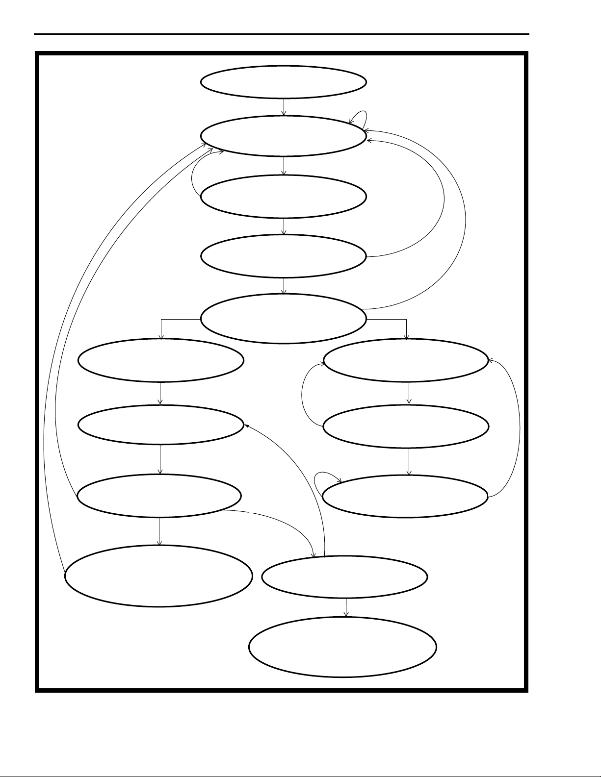
Framing Algorithm
The MT9075A contains three distinct framing
algorithms: basic frame alignment, signalling
multiframe alignment and CRC-4 multiframe
alignment. Figure 10 is a state diagram that
illustrates these algorithms and how they interact.
After power-up, the basic frame alignment framer will
search for a frame alignment signal (FAS) in the PCM
30 receive bit stream. Once the FAS is detected, the
corresponding bit 2 of the non-frame alignment
signal (NFAS) is checked. If bit 2 of the NFAS is zero
a new search for basic frame alignment is initiated. If
bit 2 of the NFAS is one and the next FAS is correct,
the algorithm declares that basic frame
synchronization has been found (i.e., page 03H,
address 10H, bit 7, SYNC is zero).
Once basic frame alignment is acquired the
signalling and CRC-4 multiframe searches will be
initiated. The signalling multiframe algorithm will
align to the first multiframe alignment signal pattern
(MFAS = 0000) it receives in the most significant
nibble of channel 16 (page 3, address 10H, bit 6,
MFSYNC = 0). Signalling multiframing will be lost
when two consecutive multiframes are received in
error.
The CRC-4 multiframe alignment signal is a 001011
bit sequence that appears in PCM 30 bit position one
of the NFAS in frames 1, 3, 5, 7, 9 and 11 (see Table
7). In order to achieve CRC-4 synchronization two
CRC-4 multiframe alignment signals must be
received without error (page 03H, address 10H, bit 5,
CRCSYN = 0) within 8 msec.
The MT9075A framing algorithm supports automatic
interworking of interfaces with and without CRC-4
processing capabilities. That is, if an interface with
CRC-4 capability, achieves valid basic frame
alignment, but does not achieve CRC-4 multiframe
alignment by the end of a predefined period, the
distant end is considered to be a non-CRC-4
interface. When the distant end is a non-CRC-4
interface, the near end automatically suspends
receive CRC-4 functions, continues to transmit CRC4 data to the distant end with its E-bits set to zero,
and provides a status indication. Naturally, if the
distant end initially achieves CRC-4 synchronization,
CRC-4 processing will be carried out by both ends.
This feature is selected when control bit AUTC (page
01H, address 11H) is set to zero.
Read Pointer
60 CH
47 CH
34 CH
Read Pointer
512 Bit
Elastic
Store
Write
Pointer
Read Pointer
2 CH
28 CH
Read Pointer
13 CH
15 CH
26 Channels
-13 CH
Figure 9 - Read and Write Pointers in the Slip Buffers
Wander Tolerance
4-149
Page 22
MT9075A Preliminary Information
Out of synchronization
>914 CRC errors
in one second
No CRC
multiframe alignment.
8 msec. timer expired*
CRC-4 multi-frame alignment
Start 400 msec timer.
Note 7.
YES
Search for primary basic frame
alignment signal RAI=1, Es=0.
YES
NO
Verify Bit 2 of non-frame
alignment signal.
YES
Verify second occurrence of
frame alignment signal.
YES
Primary basic frame synchronization
acquired. Enable traffic RAI=0, E’s=0. Start
loss of primary basic frame alignment
checking. Notes 7 & 8.
NO
3 consecutive
incorrect frame
alignment
signals
NO
Signalling multi-frame alignment
Search for multiframe
alignment signal.
Note 7.
Start 8 msec timer.
Note 7.
Basic frame
alignment acquired
Find two CRC frame
alignment signals.
Note 7.
CRC multiframe
alignment
CRC-to-CRC interworking. Re-align to new basic
frame alignment. Start CRC-4 processing. E-bits set
as per G.704 and I.431. Indicate CRC synchronization
achieved.
Notes 7& 8.
* only if CRC-4 synchronization is selected and automatic CRC-4
interworking is de-selected.
** only if automatic CRC-4 interworking is selected.
8 msec.
timer expired**
NO
Multiframe synchronization
acquired as per G.732.
NO
No CRC
multiframe
alignment.
Parallel search for new basic frame
alignment signal.
Notes 6 & 7.
CRC-to-non-CRC interworking. Maintain primary
basic frame alignment. Continue to send CRC-4
data, but stop CRC processing. E-bits set to ‘0’.
Indicate CRC-to-non-CRC operation. Note 7.
Check for two consecutive errored
multiframe alignment signals.
400 msec timer expired
YES
Note 7.
YES
Notes 7 & 8.
4-150
Figure 10 - Synchronization State Diagram
Page 23

Preliminary Information MT9075A
Notes for Synchronization State Diagram
(Figure 10)
1) The basic frame alignment, signalling multiframe
alignment, and CRC-4 multiframe alignment
functions operate in parallel and are independent.
2) The receive channel associated signalling bits and
signalling multiframe alignment bit will be frozen
when multiframe alignment is lost.
3) Manual re-framing of the receive basic frame
alignment and signalling multiframe alignment functi-
ons can be performed at any time.
4) The transmit RAI bit will be one until basic frame
alignment is established, then it will be zero.
5) E-bits can be optionally set to zero until the
equipment interworking relationship is established.
When this has been determined one of the following
will take place:
a) CRC-to-non-CRC operation - E-bits = 0,
b) CRC-to-CRC operation - E-bits as per G.704 and
I.431.
6) All manual re-frames and new basic frame
alignment searches start after the current frame
alignment signal position.
7) After basic frame alignment has been achieved,
loss of frame alignment will occur any time three
consecutive incorrect basic frame alignment signals
are received. Loss of basic frame alignment will reset
the complete framing algorithm.
8) When CRC-4 multiframing has been achieved, the
primary basic frame alignment and resulting
multiframe alignment will be adjusted to the basic
frame alignment determined during CRC-4
synchronization. Therefore, the primary basic frame
alignment will not be updated during the CRC-4
multiframing search, but will be updated when the
CRC-4 multiframing search is complete.
Channel Signalling
When control bit TxCCS (page 01H, address 1AH) is
set to one, the MT9075A is in Common Channel
Signalling (CCS) mode. When TxCCS is low it is in
Channel Associated Signalling mode (CAS). The
CAS mode ABCD signalling nibbles can be passed
either via the micro-ports (when page 01H, address
1AH, bit 3, RPSIG = 1) or through related channels
of the CSTo and CSTi serial links (when RPSIG = 0).
Memory page 05H contains the receive ABCD
nibbles and page 06H the transmit ABCD nibbles for
micro-port CAS access.
In CAS operation an ABCD signalling bit debounce
of 14 msec. can be selected by writing a one to
DBNCE (page 02H, address 10H, bit 0)). This is
consistent with the signalling recognition time of ITUT Q.422. It should be noted that there may be as
much as 2 msec. added to this duration because
signalling equipment state changes are not
synchronous with the PCM 30 multiframe.
If multiframe synchronization is lost (page 03H,
address 10H, bit 6, MFSYNC = 1) all receive CAS
signalling nibbles are frozen. Receive CAS nibbles
will become unfrozen when multiframe
synchronization is acquired.
When the CAS signalling interrupt is unmasked
(page 01H, address 1CH, bit 0, SIGI=0), pin IRQ (pin
12 in PLCC, 85 in MQFP) will become active when a
signalling nibble state change is detected in any of
the 30 receive channels. The SIGI interrupt vector
(page 04H, address 12H) is 01H.
In CCS mode the data transmit on channel 16 is
either sourced from channel 16 data on DSTi or from
the pin CSTi. If 64KCCS (page 01H, address 1AH,
bit 0) is zero the data is sourced from DSTi. If
64KCCS is high data destined for channel 16 is
clocked in from CSTi (pin 6 in PLCC, pin 71 in
MQFP) with an internal 64 KHz clock divided down
from C4b. Data received from channel 16 is clocked
out on CSTo (pin 5 in PLCC, pin 70 in MQFP). By
dividing down the extracted 2.048 MHz clock, a 64
kHz receive clock synchronous with the data is
created. This signal is output on Rx64KCK (pin 47 in
PLCC, pin 35 in MQFP).
Loopbacks
In order to meet PRI Layer 1 requirements and to
assist in circuit fault sectionalization, the MT9075A
has six loopback functions. The control bits for
digital, remote, ST-BUS, payload and metallic
loopbacks are located on page 01H, address 15H.
The remote and local time slot loopbacks are
controlled through control bits 5 and 4 of the Per
Time Slot Control Words on pages 07H and 08H.
a)
Digital Loopback
framer LIU interface. Bit DLBK = 0 normal; DLBK = 1
activate.
(DG Loop) - DSTi to DSTo at the
4-151
Page 24
MT9075A Preliminary Information
slots to the transmit PCM 30 time slots. Local time
MT9075A
DSTi
System
DSTo
b)
Remote Loopback
(RM Loop) - RTIP and RRING
Tx
PCM30
to TTIP and TRING respectively at the PCM 30 side.
Bit RLBK = 0 normal; RLBK = 1 activate.
slot loopback bit LTSL = 0 normal; LTSL = 1 activate,
will loop around DSTi time slots towards the DSTo
time slots.
MT9075A
System
DSTi
DSTo
Tx
PCM30
Rx
MT9075A
System
DSTo
c)
ST-BUS Loopback
(ST Loop) - DSTi to DSTo at
Tx
PCM30
Rx
the system side. Bit SLBK = 0 normal; SLBK = 1
activate.
MT9075A
DSTi
System
DSTo
d)
Payload Loopback
(PL Loop) - RTIP and RRING
Tx
PCM30
to TTIP and TRING respectively at the system side
with FAS and NFAS operating normally. Bit PLBK = 0
normal; PLBK = 1 activate. The payload loopback is
effectively a physical connection of DSTo to DSTi
within the MT9075A. Channel zero and the DL
originate at the point of loopback.
MT9075A
DSTi
System
DSTo
e)
Metallic Loopback
(MT Loop) - The external
Tx
Rx
PCM30
signals RTIP and RRING are isolated from the
receiver and the analog outputs TTIP and TRING are
internally connected to the receiver analog input. Bit
MLBK = 0 normal; MLBK = 1 activate.
MT9075A
DSTi
System
DSTo
f)
Local and Remote Time Slot Loopback
Tx
Rx
PCM30
. Remote
time slot loopback control bit RTSL = 0 normal; RTSL
= 1 activate, will loop around receive PCM 30 time
Error Counters
The MT9075A has nine error counters, which can be
used for maintenance testing, an ongoing measure
of the quality of a PCM 30 link and to assist the
designer in meeting specifications such as ITU-T
I.431 and G.821. All counters can be preset or
cleared by writing to the appropriate locations. A
separate status page - “1 Second Status” on page
09H - latches the states of the following counters: Ebit Error Counter, Errored Frame Alignment Signal
Counter, Bipolar Violation Counter and CRC Error
Counter on a one second interval, coincident with
the one second status bit.
Associated with each counter is a maskable event
occurrence interrupt and a maskable counter
overflow interrupt. Overflow interrupts are useful
when cumulative error counts are being recorded.
For example, every time the frame error counter
overflow (FERO) interrupt occurs, 256 frame errors
have been receiv ed since the last FERO interrupt. All
counters are cleared and held low by programming
the counter clear bit (master control page 01H,
address 1AH, bit 2) high. Counter overflows set bits
in the counter overflow latch (page 04H, address
16H); this latch is cleared when read.
The overflow reporting latch (page 04H, address
16H) contains a register whose bits are set when
individual counters overflow. These bits stay high
until the register is read.
PRBS Error Counter (PS7-0)
There are two 8 bit counters associated with PRBS
comparison; one for errors and one for time. Any
errors that are detected in the receive PRBS will
increment the PRBS Error Rate Counter of page
04H, address 10H. Writes to this counter will clear an
8 bit counter, PSM7-0 (page 01H, address 11H)
which counts receive CRC-4 multiframes. A
maskable PRBS counter overflow (PRBSO) interrupt
(page 1, address 19H) is associated with this
counter.
4-152
Page 25

Preliminary Information MT9075A
CRC Multiframe Counter for PRBS (PSM7-0)
This eight bit counter counts receive CRC-4
multiframes. It can be directly loaded via the
microport. The counter will also be automatically
cleared in the event that the PRBS error counter is
written to by the microport. This counter is located on
page 04H, address 11H.
E-bit Counter (EC9-0)
E-bit errors are counted by the MT9075A in order to
support compliance with ITU-T requirements. This
ten bit counter is located on page 04H, addresses
13H and 14H respectively. It is incremented by single
error events, with a maximum rate of twice per CRC4 multiframe.
There are two maskable interrupts associated with
the E-bit error measurement. EBI (page 1, address
1CH) is initiated when the least significant bit of the
counter toggles, and EBO (page 01H, address 1DH)
is initiated when the counter overflows.
Jitter FIFO Counter (JFC7-0)
This is an eight bit counter that is incremented when
the FIFO read pointer comes within 4 words of an
underflow or overflow condition. During this time the
read clock will abruptly speed-up or slow-down to
avoid an overflow or underflow condition. This
counter is located on page 04H, address 15H.
Loss of Synchronization Counter (LBF7-0)
Errored FAS Counter (EFAS7-EFAS0)
An eight bit Frame Alignment Signal Error counter
EFAS7 - EFAS0 is located on page 04H address
1AH, and is incremented once for every receive
frame alignment signal that contains one or more
errors.
There are two maskable interrupts associated with
the frame alignment signal error measurement. FERI
(page 01H, address 1BH) is initiated when the least
significant bit of the errored frame alignment signal
counter toggles, and FERO (page 01H, address
1DH) is initiated when the counter changes from
FFH to 00H.
Bipolar Violation Error Counter (BPV15-BPV0)
The bipolar violation error counter will count bipolar
violations or encoding errors that are not part of
HDB3 encoding. This counter BPV15-BPV0 is 16
bits long (page 04H, addresses 1DH and 1CH) and
is incremented once for every BPV error received. It
should be noted that when presetting or clearing the
BPV error counter, the least significant BPV counter
address should be written to before the most
significant location.
There are two maskable interrupts associated with
the bipolar violation error measurement. BPVI (page
01H, address 1CH) is initiated when the least
significant bit of the BPV error counter toggles.
BPVO (page 01H, address 1BH) is initiated when the
counter changes from FFFFH to 0000H.
This eight bit counter increments with each loss of
basic frame alignment. This programmable counter
is located on page 04H, address 17H.
Bit Error Rate Counter (BR7-BR0)
An 8 bit Error Rate (BERT) counter BR7 - BR0 is
located on page 04H address 18H, and is
incremented once for every bit detected in error on
either the seven frame alignment signal bits.
There are two maskable interrupts associated with
the bit error rate measurement. BERI (page 01H,
address 1CH) is initiated when the least significant
bit of the BERT counter (BR0) toggles, and BERO
(page 01H, address 1DH) is initiated when the BERT
counter value changes from FFH to 00H.
CRC Error Counter (CC9-0)
CRC-4 errors are counted by the MT9075A in order
to support compliance with ITU-T requirements. This
ten bit counter is located on page 04H, addresses
1EH and 1FH respectively. It is incremented by
single error events, which is a maximum rate of twice
per CRC-4 multiframe.
There is a maskable interrupts associated with the
CRC error measurement. CRCI (page 01H, address
1CH) is initiated when the least significant bit of the
counter toggles, and CRCO (page 01H, address
1DH) is initiated when the counter overflows.
Error Insertion
Six types of error conditions can be inserted into the
transmit PCM 30 data stream through control bits,
which are located on page 02H, address 10H. These
error events include the bipolar violation errors
4-153
Page 26

MT9075A Preliminary Information
(BPVE), CRC-4 errors (CRCE), FAS errors (FASE),
NFAS errors (NFSE), payload (PERR) and a loss of
signal error (LOSE). The LOSE function overrides
the HDB3 encoding function.
Per Time Slot Control
There are two per time slot control pages (page 07H
and 08H) occupying a total of 32 unique addresses.
Each address controls a matching timeslot on the 32
transmit channels (onto the line) and the equivalent
channel data on the receive (DSTo) data. For
example, address 0 of the first per time slot control
page contains program control for transmit timeslot 0
and DSTo channel 0.
Per Time Slot Looping
Any channel or combination of channels may be
looped from transmit (sourced from DSTi) to receive
(output on DSTo) STBUS channels. When bit 4
(LTSL) in the Per Time Slot Control Word is set the
data from the equivalent transmit timeslot is looped
back onto the equivalent receive channel.
Any channel or combination of channels may be
looped from receive (sourced from the line data) to
transmit (output onto the line) channels. When bit 5
(RTSL) in the Per Time Slot Control Word is set the
data from the equivalent receive timeslot is looped
back onto the equivalent transmit channel.
PRBS Testing
If the control bit ADSEQ is zero (from master control
page 02H address 13H - Access Control Word), any
channel or combination of transmit channels may be
programmed to contain a generated pseudo random
bit sequence (215-1). The channels are selected by
setting bit 3 (TTST) in the Per Time Slot Control
Word.
If the control bit ADSEQ is zero any combination of
receive channels may be connected to the PRBS
decoder (215-1). Each error in the incoming
sequence causes the PRBS error counter to
increment. The receive channels are selected by
setting bit 2 (RRST) in the Per Time Slot Control
Word.
A-law Milliwatt
If the control bit ADSEQ is one (from master control
page 02H - access control word), the A-law digital
milliwatt sequence (Table 10), defined by G.711, is
available to be transmit on any combination of
selected channels. The channels are selected by
setting bit 3 (TTST), in the Per Time Slot Control
Word.
The same sequence is available to replace received
data on any combination of DSTo channels. This is
accomplished by setting bit 2 (RRST) in the Per Time
Slot Control Word for the corresponding channel.
Bit 1 Bit 2 Bit 3 Bit 4 Bit 5 Bit 6 Bit 7 Bit 8
00110100
00100001
00100001
00110100
10110100
10100001
10110001
Table 10 - A-Law Digital Milliwatt Pattern
Message Mode
The transmit data on any of the transmit channels
may be sourced either from the equivalent DSTi
channel or from a dual port RAM programmed by the
microport. The address of each dual port RAM
memory location is uniquely associated with a
transmit channel number . When bit 7 (TXMSG) in the
Per Time Slot Control Word for that channel is set
the transmit data for the channel is sourced from
within the transmit message page dual port RAM (on
page 0FH and 10H).
Receive data may also be read by the
microprocessor port. The Rx message mode dual
port RAMs (on page 11H and 12H) have a unique
address associated with each incoming line channel.
When the processor reads any of the 32 memory
locations, it reads the last byte received from the
corresponding channel.
Alarms
If the PRBS testing is performed in a metallic or
external looparound the Per Time Slot Control Words
with TTST (transmit test, bit 3) set should have
RRST (receive test, bit 2) set at the same time.
4-154
The following alarms are detected by the receiver.
Each may generate a maskable interrupt:
• Remote Alarm Indication (RAI) - bit 3 (A) of
the receive NFAS;
Page 27

Preliminary Information MT9075A
• Alarm Indication Signal (AIS) - unframed all
ones signal for at least a double frame (512
bits) or two double frames (1024 bits);
• Channel 16 Alarm Indication Signal - all ones
signal in channel 16;
• Auxiliary pattern - 101010... pattern for at
least 512 bits;
• Loss of Signal - a loss of signal condition
occurs when the receive signal is detected
with more than 255 consecutive zeros. A
loss of signal condition will terminate when
an average ones density of at least 12.5%
has been received over a period of 255
contiguous pulse positions starting with a
pulse.
• Remote Signalling Multiframe Alarm - bit 6
(Y-bit) of the multiframe alignment signal.
• T1 - (T1 timer bit on page 03H address 12H)
this status bit (and maskable interrupt) shall
be high when a signal that is not normal has
been received for a minimum of 100 msec.
This bit will be low when a normal signal is
being received.
• T2 - (T2 timer bit on page 03H address 12H)
this status bit (and maskable interrupt) shall
be high when a normal signal has been
received for a minimum of 10 msec. This bit
will be low when an abnormal signal is being
received.
The alarm reporting latch (address 1BH page 04H)
contains a register whose bits are set high for
selected alarms. These bits stay high until the
register is read. This allows the controller to record
intermittent or sporadic alarm occurrences.
Automatic Alarms
12H) will go high. After the interrupt vector is read it
is automatically cleared and IRQ will return to a high
impedance state. The interrupt acknowledgment
function can also be accomplished by toggling the
INTA bit (page 01H, address 1AH).
All the interrupts of the MT9075A are maskable. This
is accomplished through the corresponding interrupt
mask words on page 01H (except for the HDLC
interrupt mask registers which are located on page
0BH and 0CH).
National Use Bit Interrupt Mask Word (address 19H)
Bit 7 Bit 0
- - - PRBSO PRBS SanibI SabitI
Interrupt Mask Word Zero (address 1BH)
C8Sa6I
Sa6I Sa5I
Bit 7 Bit 0
SYNI RAII AISI AISI6I LOSI FERI BPVO SLPI
Interrupt Mask Word One (address 1CH)
Bit 7 Bit 0
EBI CRCI CEFI BPVI RCR1 RCR0 BERI SIGI
Interrupt Mask Word Two (address 1DH)
Bit 7 Bit 0
EBO CRCO CALNI FERO JAI BERO AUXPI CMFO
Interrupt Mask Word Three (address 1EH)
Bit 7 Bit 0
MFSYI CSYNI - - - YI 1SEC T1I T2I - - -
The signalling multiframe alarm can be made to
function automatically from control bit AUTY (page
01H, address 11H). When AUTY = 0 and signalling
multiframe alignment is not acquired (page 03H,
address 10H, bit 6, MFSYNC = 1), the MT9075A will
automatically transmit the multiframe alarm (Y-bit)
signal to the far end of the link. This transmission will
cease when signalling multiframe alignment is
acquired.
Interrupts
The MT9075A has an extensive suite of maskable
interrupts, which are divided into eight categories
based on the type of event that caused the interrupt.
Each interrupt category has an associated interrupt
vector described in Table 11. When unmasked
interrupts occur, IRQ will go low and one or more bits
of the interrupt vector IV7-IV0 (page 04H, address
HDLC Interrupt Masks (page 0BH&0CH, address 16H)
Bit 7 Bit 0
Ga EOPD TEOP EopR TxFl FATxU RxFf RxOv
After a device reset (RESET pin or RST control bit),
interrupts from the following interrupt mask words
are masked:
• National use bit interrupt mask word
• Interrupt mask words one through three.
• HDLC interrupt mask word.
and the interrupts of mask word zero are unmasked.
4-155
Page 28

MT9075A Preliminary Information
All interrupts may be suspended, without changing
the interrupt mask words, by making the SPND
control bit (page 01H, address 1AH) high. Also,
when pin TAIS is held low, all interrupts are
suspended automatically. This allows for system
initialization without spurious interrupts.
Interrupt
Category and
Vector
Synchronization
D7 D0
10000000
Interrupt Description
SYNI - Loss of Synchronization.
MFSYI - Loss of Multiframe Sync.
CSYNI - Loss of CRC-4 Sync.
YI - Remote Multiframe Sync. Fail.
Alarm
D7 D0
01000000
Counter
Indication
D7 D0
00100000
Counter
Overflow
D7 D0
00010000
One Second
D7 D0
00001000
RAII - Remote Alarm Indication.
AISI - Alarm Indication Signal.
AIS16I - AIS on Channel 16.
LOSI - Loss of Signal.
AUXPI - Auxiliar y Pattern.
EBI - Receive E-bit Error.
CRCI - CRC-4 Error.
CEFI - Consecutive Errored FASs.
FERI - Frame Alignment Signal
Error.
BPVI - Bipolar Violation Error.
RCR0 - RAI and CRC Error Active.
RCR1 - RAI and CRC Error End.
BERI - Bit Error.
EBO - Receive E-bit Error.
CRCO - CRC-4 Error.
FERO - Frame Alignment Signal.
BPVO - Bipolar Violation.
BERO - Bit Error.
CMFO - CRC-4 Multiframe.
1SECI - One Second Timer.
CALNI - CRC-4 Multiframe
Alignment.
T1I - Timer T1 expires.
T2I - Timer T2 expires.
SLIP
D7 D0
SLPI - Receive Slip.
JAI - Jitter Attenuator Error.
00000100
National Use/
HDLC0
D7 D0
00000010
PRBSO-PRBS Error Counter
Overflow
PRBSI - PRBS Single Error
SanibI - Changed S
SabitI - Changed S
C8SA6I- Sequence of 8 S
SA6I - Changed S
SA5I - Changed S
a6
a5
HDLC0 - Status
Signalling/
HDLC1
D7 D0
SIGI-Receive Signalling Bit
Change.
HDLC1 - Status.
00000001
Table 11 - MT9075A Interrupt Vectors
(IV7 - IV0)
a5,6,7 or 8
a5,6,7 or 8
a6
nibbles.
bits.
Nibble
Bits
nibbles.
4-156
Page 29

Preliminary Information MT9075A
Control and Status Registers
Master Control 1 (Page 01H)
Address
(A4A3A2A1A0)
10H (Table 13) Multiframe, National Bit Buffer and Data
Link Selection Word
11H (Table 14) Mode Selection Control Word TIU0, CRCM, RST, AUTY, TxTRSP, CSYN &
12H (Table 15) Non-Frame Alignment Control Word TIU1, TALM & TNU4-8
13H (Table 16) Transmit Multiframe Alignment Signal TMA1-4, X1, Y, X2 & X3
14H (Table 17) HDLC Selection Word HDLC0, HDLC1, RxTRSP
15H (Table 18) Coding and Loopback Control Word MLBK, HDB3, MFRF, DLBK, RLBK, SLBK &
16H (Table 19) Transmit Alarm Control Word TAIS, TAIS0, TAIS16, TE, REFRM, 64KSEL,
17H Reserved Set all bits to zero for normal operation.
18H --- Unused.
19H (Table 20) National Use Bit Interrupt Mask Word PRBSO,PRBSI,SanibI,SabitI,C8Sa6I, Sa6I, Sa5I
1AH (Table 21) Interrupt, Signalling and BERT Control
Word
Register Names
ASEL, MFSEL, NBTB & Sa4 - S
AUTC
PLBK
DSToDE & CSToDE
ODE, SPND, INTA, TxCCS, RPSIG, CNTCLR
& MSN, 64KCCS
a8
1BH (Table 22) Interrupt Mask Word Zero SYNI, RAII, AISI, AIS16I, LOSI, FERI, BPVO &
SLPI
1CH (Table 23) Interrupt Mask Word One EBI, CRCI, CEFI, BPVI, RCR0I, RCR1I, BERI
& SIGI
1DH (Table 24) Interrupt Mask Word Two EBOI, CRCOI, CALNI, FEROI, JAI, BEROI,
AUXPI & CMFOI
1EH (Table 25) Interrupt Mask Word Three MFSYI, CSYNI, YI, 1SECI, T1I, T2I
1FH (Table 26) Transmit Pulse Control Word LL0, LL1, LL2
Table 12 - Master Control 1 (Page 01H)
4-157
Page 30

MT9075A Preliminary Information
Bit Name Functional Description
7 ASEL AIS Select. This bit selects the
criteria on which the detection of a
valid Alarm Indication Signal (AIS)
is based. If zero, the criteria is less
than three zeros in a two frame
period (512 bits). If one, the criteria
is less than three zeros in each of
two consecutive double-frame
periods (512 bits per double-frame).
6 MFSEL Multiframe Select. This bit
determines which receive
multiframe signal (CRC-4 or
signalling) the RxMF (pin 42 in
PLCC, 23 in MQFP) signal is
aligned with. If zero, RxMF is
aligned with the receive signalling
multiframe. If one, RxMF is aligned
with the receive CRC-4 multiframe.
5 NBTB National Bit Transmit Buffer. If
one, the transmit NFAS signal
originates from the transmit national
bit buffer; if zero, the transmit NFAS
signal originates from the TNU4-8
bits of page 01H, address 12H.
Bit Name Functional Description
7 TIU0 Transmit International Use Zero.
When CRC-4 operation is disabled
(CSYN=1), this bit is transmit on
the PCM 30 2048 kbit/sec. link in
bit position one of time-slot zero of
frame-alignment frames. It is
reserved for international use and
should normally be kept at one. If
CRC processing is used, i.e.,
CSYN =0, this bit is ignored.
6 CRCM CRC-4 Modification. If one,
activates the CRC-4 remainder
modification function when the
device is in transparent mode. The
received CRC-4 remainder is
modified to reflect only the changes
in the transmit DL. If zero, time slot
zero data from DSTi will not be
modified in transparent mode.
5 RST Reset. When this bit is changed
from zero to one the device will
reset to its default mode. See the
Reset Operation section for the
default settings.
4 - 0 Sa4 - Sa8A one selects the corresponding S
bits of the NFA signal for 4, 8, 12,
16 or 20 kbits/sec. data link
channel. Data link (DL) selection will
function in termination mode only; in
transmit transparent mode Sa4 is
automatically selected - see
TxTRSP control bit of page 01H,
address 11H. If zero, the
corresponding bits of transmit nonframe alignment signal are
programmed by the Non-Frame
Alignment Control Word (page
01H, address 12H).
Table 13 - Multiframe National Bit Buffer and DL
Selection Word (Page 01H, Address 10H)
a
4 --- Unused. Set high for normal
operation.
3 AUTY Automatic Y-Bit Operation. If
zero, the Y-bit of the transmit
multiframe alignment signal will
report the multiframe alignment
status to the far end i.e., zero multiframe alignment acquired, one
- lost. If one, the Y-bit is under the
manual control of the Transmit
Multiframe Alignment Control
Word.
2 TxTRSP Transmit Transparent Mode. If
one, the MT9075A is in transmit
transparent mode. No framing or
signaling is imposed on the data
transmit from DSTi onto the line. If
zero, it is in termination mode.
Table 14 - Mode Selection Control Word
(Page 01H, Address 11H)
4-158
Page 31

Preliminary Information MT9075A
1 CSYN CRC-4 Synchronization. If zero,
basic CRC-4 synchronization
processing is activated, and TIU0
bit and TIU1 bit programming will
be overwritten. If one, CRC-4
synchronization is disabled, the
first bits of channel 0 are used as
international use bits and are
programmed by TIU0 and TIU1.
0 AUTC Automatic CRC-interworking. If
zero, automatic CRC-interworking
is activated. If one, it is deactivated.
See Framing Algorithm section for
a detail description.
Table 14 - Mode Selection Control Word
(Page 01H, Address 11H)
Bit Name Functional Description
7 TIU1 Transmit International Use One.
When CRC-4 operation is disabled
(CSYN=1), this bit is transmit on the
PCM 30 2048 kbit/sec. link in bit
position one of time-slot zero of
non-frame-alignment frames. It is
reserved for international use and
should normally be kept at one. If
CRC processing is used, i.e., CSYN
=0, this bit is ignored.
6 - - - Unused. Set low for normal
operation.
5 TALM Transmit Remote Alarm. This bit is
transmitted on the PCM 30 2048
kbit/sec. link in bit position three (A
bit) of time slot zero of NFAS
frames. It is used to signal an alarm
to the remote end of the PCM 30
link (one - alarm, zero - normal).
This control bit is ignored when
ARAI is zero (page 01H, address
11H).
Bit Name Functional Description
7 -4 TMA1-4 Transmit Multiframe Alignment
Bits One to Four. These bits are
transmitted on the PCM 30 2048
kbit/sec. link in bit positions one to
four of time slot 16 of frame zero of
every signalling multiframe. These
bits are used by the far end to
identify specific frames of a
signalling multiframe. TMA1-4 =
0000 for normal operation.
3 X1 This bit is transmitted on the PCM
30 2048 kbit/sec. link in bit position
five of time slot 16 of frame zero of
every multiframe. X1 is normally
set to one.
2 Y This bit is transmitted on the PCM
30 2048 kbit/sec. link in bit position
six of time slot 16 of frame zero of
every multiframe. It is used to
indicate the loss of multiframe
alignment to the remote end of the
link. If one - loss of multiframe
alignment; if zero - multiframe
alignment acquired. This bit is
ignored when AUTY is zero (page
01H, address 11H).
1 - 0 X2, X3 These bits are transmitted on the
PCM 30 2048 kbit/sec. link in bit
positions seven and eight
respectively, of time slot 16 of
frame zero of every multiframe. X2
and X3 are normally set to one.
Table 16 - Transmit MF Alignment Signal
(Page 01H, Address 13H)
4 -0 TNU4-8 Transmit National Use Four to
Eight (Sa4 - Sa8). These bits are
transmitted on the PCM 30 2048
kbit/sec. link in bit positions four to
eight of time slot zero of the NFA
frame, if selected by Sa4 - S
control bits of the DL selection word
(page 01H, address 10H).
T able 15 - NF A Control W ord
(page 01H, Address 12H)
a8
4-159
Page 32

MT9075A Preliminary Information
Bit Name Functional Description
7 HDLC0 HDLC0 Select. If one, then HDLC0
is connected to the data link on
selected Sa bits at a rate of 4, 8, 12,
16 or 20 kbits/sec. If zero, HDLC0 is
deselected and all HDLC0 interrupts
are masked.
6 HDLC1 HDLC1 Select. If one, then HDLC1
is connected to time slot 16 in CCS
mode. If zero, HDLC1 is deselected
and all HDLC1 interrupts are
masked.
5 RxTRSP Receive Transparent Mode. When
this bit is set to one, the framing
function is disabled on the receive
side. Data coming from the receive
line passes through the slip buffer
and drives DSTo with an arbitrary
alignment. When zero, the receive
framing function operates normally.
4-0 --- Unused.
Table 17 - HDLC Selection Word
(Page 01H, Address 14H)
Bit Name Functional Description
7 --- Unused.
6 MLBK Metallic Loopback. If one, then the
external RRTIP and RRING signals
are isolated from the receiver, and
TTIP and TRING are internally
connected to the receiver analog
input instead. If zero, metallic
loopback is disabled.
5 HDB3 High Density Bipolar 3 Encoding.
If zero, HDB3 encoding is enabled
in the transmit direction. If one, AMI
signal without HDB3 encoding is
transmitted. HDB3 is always
decoded in the receive direction.
4 MFRF Multiframe Reframe. If one, for at
least one frame, and then cleared
the MT9075A will initiate a search
for a new signalling multiframe
position. Reframing function is
activated on the one-to-zero
transition of the MFRF bit.
3 DLBK Digital Loopback. If one, then the
digital stream to the transmit LIU is
looped back in place of the digital
output of the receive LIU. Data
coming out of DSTo will be a
delayed version of DSTi. If zero, this
feature is disabled.
2 RLBK Remote Loopback. If one, then all
bipolar data received on RRTIP/
RRING are directly routed to TTIP/
TRING on the PCM 30 side of the
MT9075A. If zero, then this feature
is disabled.
1 SLBK ST-BUS Loopback. If one, then all
time slots of DSTi are connected to
DSTo on the ST-BUS side of the
MT9075A. If zero, then this feature
is disabled. See Loopbacks section.
0 PLBK Payload Loopback. If one, then all
time slots received on RTIP/RRING
are connected to TTIP/TRING on
the ST-BUS side of the MT9075A
(this excludes time slot zero). If
zero, then this feature is disabled.
Table 18 - Coding and Loopback Control Word
(Page 01H, Address 15H)
4-160
Page 33

Preliminary Information MT9075A
Bit Name Functional Description
7 TAIS Transmit Alarm Indication Signal.
If one, an all ones signal is
transmitted. TAIS=0 for normal
operation.
6 TAIS0 Transmit AIS Time Slot Zero. If
one, an all ones signal is
transmitted in time slot zero. If zero,
time slot zero functions normally.
5 TAIS16 Transmit AIS Time Slot 16. If one,
an all ones signal is transmitted in
time slot 16. If zero, time slot
functions normally.
4TETransmit E bits. When zero and
CRC-4 synchronization is
achieved, the E-bits transmit the
received CRC-4 comparison results
to the distant end of the link, as per
G.704. That is, when zero and
CRC-4 synchronization is lost, the
transmit E-bits will be zero. If one,
and CRC-4 synchronization is lost
the transmit E-bits will be one.
3 REFRM Reframe. If one for at least one
frame, and then cleared, the device
will initiate a search for a new basic
frame position. Reframing function
is activated on the one-to-zero
transition of the REFRM bit.
2 64KSEL 64 KHz Select. If one, a 64 KHz
signal divided down from the
extracted received 2048 kbit/sec.
clock is output on RxFP/Rx64KCK
(pin 47 in PLCC, 35 in MQFP). If
zero that pin outputs an 8 KHz
signal derived from the extracted
clock.
1 DSToDE DSTo Data Enable. If zero, DSTo is
enabled. If one, DSTo will be
tristated if one of the following
conditions exists: LIU loss of signal,
loss of terminal frame sync
(SYNC=1), loss of CRC4 sync
(CRCSYN=1) or AIS.
0 CSToDE CSTo Data Enable. If zero, CSTo is
enabled. If one, CSTo will be
tristated if one of the following
conditions exists: loss of multiframe
sync (MFSYNC=1), or AIS16 =1
Bit Name Functional Description
7 --- Unused.
6 PRBSO PRBS Counter Overflow
Interrupt. When unmasked
(PRBSO = 1), an interrupt is
initiated on overflow of PRBS
counter (page 04H, address 10H)
from FFH to 0H. Interrupt vector =
00000010.
5 PRBSI PRBS Interrupt. When unmasked
(PRBSI = 1), an interrupt is initiated
on a single PRBS detection error.
Interrupt vector = 00000010.
4S
nibI Changed Sa Nibble Interrupt.
a
When unmasked (SanibI = 1), an
interrupt is generated upon
detection of a change of state in any
of received Sa nibbles (nibble Sa5,
nibble Sa6, nibble Sa7 or nibble Sa8).
Interrupt vector = 00000010.
3S
bitI Changed Sa Bit Interrupt. When
a
unmasked (SabitI = 1), an interrupt
is generated upon detection of a
change of state in any of received
Sa bits (Sa5, Sa6, Sa7 or Sa8).
Interrupt vector = 00000010.
2 C8Sa6I Eight Consecutive Sa6 Nibble
Interrupt. When unmasked (C8Sa6I
= 1), an interrupt is generated upon
detection of the eighth consecutive
Sa6 nibble with the same pattern.
Interrupt vector = 00000010.
1Sa6I Changed Sa6 Nibble Interrupt.
When unmasked (Sa6I = 1), an
interrupt is generated upon
detection of a change of state in
received Sa6 nibbles. Interrupt
vector = 00000010.
0Sa5I Changed Sa5 Bit Interrupt. When
unmasked (Sa5I =1), an interrupt is
generated upon detection of a
change of state in the received S
a5
bit. Interrupt vector = 00000010.
Table 20 - National Use Bit Interrupt Mask Word
(Page 01H, Address 19H)
Table 19 - Transmit Alarm Control Word
(Page 01H, Address 16H)
4-161
Page 34

MT9075A Preliminary Information
Bit Name Functional Description
7 ODE Output Data Enable. If one, the
DSTo and CSTo output drivers
function normally. When low, DSTo
and CSTo will be tristated.
Note: When ODE =1, DSTo and
CSTo can be individually tristated
by DSToDE and CSToDE (page
01H, address 16H) respectively.
6 SPND Suspend Interrupts. If one, the
IRQ output (pin 12 in PLCC, 85 in
MQFP) will be in a high-impedance
state and all interrupts will be
ignored. If zero, the IRQ output will
function normally.
5 INTA Interrupt Acknowledge. A zero-to-
one or one-to-zero transition will
clear any pending interrupt and
make IRQ high.
4 TxCCS Transmit Common Channel
Signalling. If one, the transmit
section of the device is in common
channel signalling (CCS) mode. If
zero, it is in Channel Associated
Signalling (CAS) mode.
3 RPSIG Register Programmed
Signalling. If one, the transmit CAS
signalling will be controlled by
programming page 05H. If zero, the
transmit CAS signalling will be
controlled through the CSTi stream.
Table 21 - Interrupt, Signalling and BERT
Control Word (Page 01H, Address 1AH)
(continued)
Bit Name Functional Description
CNTCLR
2
1 MSN Most Significant Signalling
64KCCS
0
Table 21 - Interrupt, Signalling and BERT
Control Word (Page 01H, Address 1AH)
Counter Clear. If one, all status
counters are cleared and held low.
Zero for normal operation.
Nibble. If one, the CSTo and CSTi
channel associated signalling
nibbles will be valid in the most
significant portion of each ST-BUS
time slot. If zero, the CSTo and
CSTi channel associated signalling
nibbles will be valid in the least
significant portion of each ST-BUS
time slot.
64 Kbits/s Common Channel
Signalling. If one, common channel
signalling information is sourced
from CSTi, and common channel
signalling information is clocked out
of CSTo. The transmit clock is an
internal clock. This 64 KHz clock is
divided down from C4b and is
synchronous with the STBUS
channel boundaries. The rising
edges of the clock occur between
channels 1 and 2; 5 and 6; 9 and
10; 13 and 14; 17 and 18; 21 and
22; 25 and 26; 29 and 30. The
receive clock is synchronous with
the same channel times, but derived
from the extracted clock timebase.
The CCS receive clock is driven out
on Rx64KCK (pin 47 in PLCC, 35 in
MQFP) when this bit is set.
4-162
Page 35

Preliminary Information MT9075A
Bit Name Functional Description
7 SYNI Synchronization Interrupt. When
unmasked (SYNI = 0) an interrupt is
initiated when a loss of basic frame
synchronization condition exists.
Interrupt vector = 10000000.
6 RAII Remote Alarm Indication
Interrupt. When unmasked (RAII
= 0) a received RAI will initiate an
interrupt. Interrupt vector =
01000000.
5 AISI Alarm Indication Signal Interrupt.
When unmasked (AISI = 0) a
received AIS will initiate an
interrupt. Interrupt vector =
01000000.
4 AIS16I Channel 16 Alarm Indication
Signal Interrupt. When unmasked
(AIS16I = 0), a received AIS16 will
initiate an interrupt. Interrupt vector
= 01000000.
3 LOSI Loss of Signal Interrupt. When
unmasked (LOSI = 0) an interrupt is
initiated when a loss of signal
condition exists. Interrupt vector =
01000000.
2 FERI Frame Error Interrupt. When
unmasked (FERI = 0), an interrupt
is initiated when an error in the
frame alignment signal occurs.
Interrupt vector = 00100000.
1 BPVO Bipolar Violation Counter
Overflow Interrupt. When
unmasked (BPVO = 0), an interrupt
is initiated when the bipolar violation
error counter changes form FFFFH
to 0H. Interrupt vector = 00010000.
0 SLPI SLIP Interrupt. When unmasked
(SLPI = 0), an interrupt is initiated
when a controlled frame slip occurs.
Interrupt vector = 00000100.
Table 22 - Interrupt Mask Word Zero
(Page 01H, Address 1BH)
Bit Name Functional Description
7 EBI Receive E-bit Interrupt. When
unmasked an interrupt is initiated
when a receive E-bit indicates a
remote CRC-4 error. 1 unmasked, 0 - masked. Interrupt
vector = 00100000.
6 CRCI CRC-4 Error Interrupt. When
unmasked an interrupt is initiated
when a local CRC-4 error occurs. 1
- unmasked, 0 - masked. Interrupt
vector = 00100000.
5 CEFI Consecutively Errored FASs
Interrupt. When unmasked an
interrupt is initiated when two
consecutive errored frame
alignment signals are received. 1 unmasked, 0 - masked. Interrupt
vector = 00100000.
4 BPVI Bipolar Violation Interrupt. When
unmasked an interrupt is initiated
when a bipolar violation error
occurs. 1 - unmasked, 0 - masked.
Interrupt vector = 00100000.
3 RCR0I RAI and Continuous CRC Error
Interrupt. When unmasked an
interrupt is initiated when the
received A bit has been one, and
the received E bits have been zero,
continuously for greater than 10
milliseconds (see page 04H,
address 19H) 1- unmasked, 0 masked. Interrupt vector =
00100000.
2 RCR1I RAI and Continuous CRC Error
Interrupt. When unmasked an
interrupt is initiated when the
received A bit had been set, and the
received E bits were low,
continuously for greater than 10
milliseconds, but less than 450
milliseconds (see page 04H,
address 19H). 1 - unmasked, 0 masked. Interrupt vector =
00100000.
1 BERI Bit Error Interrupt. When
unmasked an interrupt is initiated
when a bit error occurs. 1 unmasked, 0 - masked. Interrupt
vector = 00100000.
Table 23 - Interrupt Mask Word One
(Page 01H, Address 1CH) (continued)
4-163
Page 36

MT9075A Preliminary Information
Bit Name Functional Description
0 SIGI Signalling (CAS) Interrupt. When
unmasked and any of the receive
ABCD bits of any channel changes
state an interrupt is initiated. 1 unmasked, 0 - masked. Interrupt
vector = 00000001
Table 23 - Interrupt Mask Word One
(Page 01H, Address 1CH)
Bit Name Functional Description
7 EBOI Receive E-bit Counter Overflow
Interrupt. When unmasked an
interrupt is initiated when the E-bit
error counter overflows. 1 unmasked, 0 - masked. Interrupt
vector = 00010000.
6 CRCOI CRC-4 Error Counter Overflow
Interrupt. When unmasked an
interrupt is initiated when the CRC-4
error counter overflows. 1 unmasked, 0 - masked. Interrupt
vector = 00010000.
Bit Name Functional Description
2 BEROI Bit Error Counter Overflow
Interrupt. When unmasked (BERO
= 1), an interrupt is initiated when
the bit error counter overflows.
Interrupt vector = 00010000.
1 AUXPI Auxiliary Pattern Interrupt. When
unmasked (AUXPI = 1), an interrupt
is initiated when the AUXP status bit
of page 03H, address 15H goes
high. Interrupt vector = 01000000.
0 CMFOI Receive CRC-4 Multiframe
Counter Overflow Interrupt. When
unmasked (CMFO = 1), an interrupt
is initiated when the CRC-4
multiframe counter overflows.
Interrupt vector = 00010000.
Table 24 - Interrupt Mask Word Two
(Page 01H, Address 1DH)
5 CALNI CRC-4 Alignment Interrupt. When
unmasked an interrupt is initiated
when the CALN status bit of page
03H, address 12H changes state. 1
- unmasked, 0 - masked. Interrupt
vector = 00001000.
4 FEROI Frame Alignment Signal Error
Counter Overflow Interrupt. When
unmasked an interrupt is initiated
when the frame alignment signal
error counter overflows. 1 unmasked, 0 - masked. Interrupt
vector = 00010000.
3 JAI Jitter Attenuation Interrupt.
When unmasked, an interrupt will
be initiated when the jitter
attenuator FIFO comes within four
bytes of an overflow or underflow
condition. 1 - unmasked, 0 masked. Interrupt vector =
00000100.
Table 24 - Interrupt Mask Word Two
(Page 01H, Address 1DH) (continued)
4-164
Page 37

Preliminary Information MT9075A
Bit Name Functional Description
7 MFSYI Multiframe Synchronization
Interrupt. When unmasked
(MFSYI = 1), an interrupt is initiated
when multiframe synchronization is
lost. Interrupt vector = 10000000.
6 CSYNI CRC-4 Multiframe
Synchronization Interrupt. When
unmasked (CSYNI = 1), an interrupt
is initiated when CRC-4 multiframe
synchronization is lost. Interrupt
vector = 10000000.
5 - - - Unused.
4YIRemote Signalling Multiframe
Alarm Interrupt. When unmasked
(YI = 1), an interrupt is initiated
when a remote signalling multiframe
alarm signal is received. Interrupt
vector = 10000000.
Table 25: Interrupt Mask Word Three
(Page 01H, Address 1EH)
Bit Name Functional Description
3 1SECI One Second Status Interrupt.
When unmasked (1SECI = 1), an
interrupt is initiated when the 1SEC
status bit (page 03H, address 12H,
bit 7) changes from zero to one.
Interrupt vector = 00001000.
2 T1I T1 Timer Interrupt. When
unmasked (T1I = 1), an interrupt is
initiated when the T1 timer bit (page
03H, address 12H, bit 5) changes
from zero to one. Interrupt vector =
00001000.
1 T2I T2 Timer Interrupt. When
unmasked (T2I = 1), an interrupt is
initiated when the T2 timer bit (page
03H, address 12H, bit 4) changes
from zero to one. Interrupt vector =
00001000.
0 - - - Unused
Table 25: Interrupt Mask Word Three
(Page 01H, Address 1EH)
Bit Name Functional Description
7-3 --- Unused. Set low for normal operation.
2-0 TX2-0 Transmit pulse amplitude. Select the
TX2-TX0 bits according to the line type,
value of termination resistors (RT), and
transformer turns ratio used
TX2 TX1 TX0 Line(Ω) RT(Ω) Xfmr
0 0 0 120 0 1:2
0 0 1 120 0 1:1
0 1 0 120 15 1:2
0 1 1 120/75 12.1 1:2
1 0 0 75 0 1:2
1 0 1 75 0 1:1
1 1 1 75 9.1 1:2
1 1 1 75/120 12.1 1:2
Table 26: Transmit Pulse Control Word
4-165
Page 38

MT9075A Preliminary Information
Address
(A4A3A2A1A0)
10H (Table 28) Error and Debounce Selection Word BPVE, CRCE, FASE, NFSE, LOSE, PERR &
11H --- Unused.
12H --- Unused.
13H (Table 29) Access Control Word LOS/LOF, ADSEQ & GCI/ST
14H --- Unused.
15H --- Unused.
16H --- Unused.
17H --- Unused.
18H (Table 30) Jitter Attenuator Control Word JAS, JAT/JAR, JFC, JFD2, JFD1, JFD0, JACL
19H (Table 31) Receive Equalization Control Word REDBL, REMID, REMAX
1AH Reserved Set all bits to zero for normal operation.
1BH Reserved Set all bits to zero for normal operation.
1CH Reserved Set all bits to zero for normal operation.
Register Names
DBNCE
1DH Reserved Set all bits to zero for normal operation.
1EH Reserved Set all bits to zero for normal operation.
1FH Reserved Set all bits to zero for normal operation.
Table 27: Master Control 2 (Page 02H)
4-166
Page 39

Preliminary Information MT9075A
Bit Name Functional Description
7 BPVE Bipolar Violation Error Insertion.
A zero-to-one transition of this bit
inserts a single bipolar violation
error into the transmit PCM 30 data.
A one, zero or one-to-zero transition
has no function.
6 CRCE CRC-4 Error Insertion. A zero-to-
one transition of this bit inserts a
single CRC-4 error into the transmit
PCM 30 data. A one, zero or one-to-
zero transition has no function.
5 FASE Frame Alignment Signal Error
Insertion. A zero-to-one transition
of this bit inserts a single error into
the time slot zero frame alignment
signal of the transmit PCM 30 data.
A one, zero or one-to-zero transition
has no function.
4 NFSE Non-frame Alignment Signal
Error Insertion. A zero-to-one
transition of this bit inserts a single
error into bit two of the time slot zero
non-frame alignment signal of the
transmit PCM 30 data. A one, zero
or one-to-zero transition has no
function.
3 LOSE Loss of Signal Error Insertion. If
one, the MT9075A transmits an all
zeros signal (no pulses) in every
PCM 30 time slot. If zero, data is
transmitted normally.
2 PERR Payload Error Insertion. A zero-to-
one transition of this bit inserts a
single error in the transmit payload.
A one, zero or one-to-zero transition
has no function.
Bit Name Functional Description
7-3 -- Unused.
2 LOS/LOF Loss of Signal or Loss of Frame
Selection. If one, pin LOS (pin 61 in
PLCC, 57 in MQFP) will go high
when a loss of signal state exits
(criteria as per LLOS status bit on
page 03H address 18H). If low, pin
LOS will go high when either a loss
of signal (LLOST =1) or a loss of
basic frame alignment state exits
(bit SYNC on page 03H address
10H is zero).
1 ADSEQ Digital Milliwatt or Digital Test
Sequence. If one, the A-law digital
milliwatt analog test sequence will
be selected by the Per Time Slot
Control bits TTST and RTST (on
page 07H and 08H). If zero, the
PRBS 215-1 bit error rate test
sequence will be selected by the
Per Time Slot Control bits TTST and
RTST. The PRBS generator is reset
whenever this bit is set to 1.
0 GCI/ST GCI or ST-BUS Frame Pulse. If
one, the MT9075A will transmit or
receive a GCI frame pulse on pin
F0b (pin 46 in PLCC, 34 in MQFP).
If zero, the MT9075A will transmit or
receive an ST-BUS frame pulse on
F0b.
Table 29 - Access Control Word
(Page 02H, Address 13H)
1 --- Unused.
0 DBNCE Debounce Select. This bit selects
the debounce period (1 for 14
msec.; 0 for no debounce). Note:
there may be as much as 2 msec.
added to this duration because the
state change of the signalling
equipment is not synchronous with
the PCM 30 signalling multiframe.
Table 28 - Error and Debounce Selection Word
(Page 02H, Address 10H)
4-167
Page 40

MT9075A Preliminary Information
Bit Name Functional Description
7 JAS Jitter Attenuator Select. If one,
the attenuator may be connected to
either the transmit or receive sides
of the PCM 30 interface depend on
bit 6 - JAT/JAR. If zero, the jitter
attenuator function is disabled.
6 JAT/JAR Transmit or Receive Jitter
Attenuator. If one, the jitter
attenuator will function on the
transmit data. If zero, the jitter
attenuator will function on the
receive data.
5 JFC Jitter Attenuator FIFO Centre.
When this bit is toggled the read
pointer of the jitter attenuator shall
be centered. During centering the
jitter in the JA outputs is increased
by 0.0625 U.I
4 - 2 JFD2-
JFD0
Jitter Attenuator FIFO Depth
Control Bits. These bits determine
the depth of the jitter attenuator
FIFO as shown below:
JFD2 JFD1 JFD0 Depth
(words)
000 16
Bit Name Functional Description
7 REDBL Receive Equalizer Auto Mode
Disable. If one, the receive
equalizer is turned off from the auto
mode. If zero, the receive equalizer
is turned on and will compensate for
loop length automatically.
6 REMID Receive Equalization Mid-range.
If one and REDBL is one, the onestage equalization is enabled, which
provides approximately 6 dB of
gain. If zero, REDBL or REMAX will
control the receive equalization.
5 REMAX Receive Equalization Maximum. If
one, REDBL is one and REMID is
zero, the two-stage equalization is
enabled, which provides
approximately 12 dB of gain. If zero,
REDBL or REMID will control the
receive equalization.
4 - 0 --- Unused.
Table 31 - Receive Equalization Control Word
(Page 02H, Address 19H)
001 32
010 48
011 64
100 80
101 96
1 1 0 112
1 1 1 128
1 JACL Jitter Attenuator Clear bit. If one,
the Jitter Attenuator, its FIFO and
status are reset. The status
registers will identify the FIFO as
being empty. However, the actual
bit values of the data in the JA
FIFO will not be reset.
0 --- Unused.
Table 30 - Jitter Attenuator Control Word
(Page 02H, Address 18H)
4-168
Page 41

Preliminary Information MT9075A
Master Status 1 (Page 03H)
Address
(A4A3A2A1A0)
10H (Table 33) Synchronization Status Word SYNC, MFSYNC, CRCSYN, REB1, REB2 CRCRF,
11H (Table 34) Receive Frame Alignment Signal RIU0 & RFA2-8
12H (Table 35) Timer Status Word 1SEC, 2SEC, T1, T2, 400T, 8T, CALN & KLVE
13H (Table 36) Receive Non-frame Alignment Signal RIU1, RNFAB, RALM & RNU4-8
14H (Table 37) Receive Multiframe Alignment Signal RMA1-4, X1, Y, X2 & X3
15H (Table 38) Most Significant Phase Status Word RSLIP, RSLPD, AUXP, CEFS, RxEBC11-8
16H (Table 39) Least Significant Phase Status Word RxEBC7-0
17H (Table 40) Jitter Attenuator Status Word JACS, JACF, JAE, JAF4, JAFC, JAE4, JAF
18H (Table 41) Receive Signal Status Word LL, ML, SL, LLOS
19H (Table 42) Alarm Status Word One CRCS1, CRCS2, RFAIL, LOSS, AIS16S, AISS,
1AH (Table 43) Changed Sa6 Report Word Sa5, Sa6nibble,C8Sa6, CS
1BH - 1EH --- Unused.
Register Names
RED& CRCIWK
RAIS & RCRS
a6
1FH (Table 44) Identification Word Set to 10101010
Table 32 - Master Status 1 (Page 03H)
4-169
Page 42

MT9075A Preliminary Information
Bit Name Functional Description
7 SYNC Receive Basic Frame Alignment.
SYNC indicates the basic frame
alignment status (1 - loss; 0 acquired).
6 MFSYNC Receive Multiframe Alignment.
MFSYNC indicates the multiframe
alignment status (1 - loss; 0 acquired).
5 CRCSYN Receive CRC-4 Synchronization.
CRCSYN indicates the CRC-4
multiframe alignment status (1 loss; 0 - acquired).
4 REB1 Receive E-Bit One Status. REB1
indicates the status of the received
E1 bit of the last multiframe.
3 REB2 Receive E-Bit Two Status. REB2
indicates the status of the received
E2 bit of the last multiframe.
2 CRCRF CRC-4 Reframe. A one indicates
that the receive CRC-4 multiframe
synchronization could not be found
within the time out period of 8 msec.
after detecting basic frame
synchronization. This will force a
reframe when the maintenance
option is selected and automatic
CRC-4 interworking is de-selected.
Bit Name Functional Description
7 RIU0 Receive International Use Zero.
This is the bit which is received on
the PCM 30 2048 kbit/sec. link in bit
position one of the frame alignment
signal. It is used for the CRC-4
remainder or for international use.
6 - 0 RFA2-8 Receive Frame Alignment Signal
Bits 2 to 8. These bit are received
on the PCM 30 2048 kbit/sec. link in
bit positions two to eight of frame
alignment signal. These bits form
the frame alignment signal and
should be 0011011.
Table 34 - Receive Frame Alignment Signal
(Page 03H, Address 11H)
1 RED RED Alarm. RED goes high when
basic frame alignment has been lost
for at least 100 msec. This bit will be
low when basic frame alignment is
acquired (I.431).
0 CRCIWK CRC-4 Interworking. CRCIWK
indicates the CRC-4 interworking
status (1 - CRC-to-CRC; 0 - CRCto-non-CRC).
Table 33 - Synchronization Status Word
(Page 03H, Address 10H)
4-170
Page 43

Preliminary Information MT9075A
Bit Name Functional Description
7 1SEC One Second Timer Status. This bit
changes state once every 0.5
second and is synchronous with the
2SEC timer. This feature is not
available when the device is
operated in freerun mode.
6 2SEC Two Second Timer Status. This bit
changes state once every second
and is synchronous with the 1SEC
timer. This feature is not available
when the device is operated in
freerun mode.
5T1Timer One. This bit will be high
upon loss of terminal frame
synchronization persisting for 100
msec. This bit shall be low when T2
becomes high. Refer to I.431
Section 5.9.2.2.3. This feature is not
available when the device is
operated in freerun mode.
4T2Timer Two. This bit will be high
when the MT9075A acquires
terminal frame synchronization
persisting for 10 msec. This bit shall
be low when non-normal
operational frames are received.
I.431 Section 5.9.2.2.3. This feature
is not available when the device is
operated in freerun mode.
3 400T 400 msec. Timer Status. This bit
changes state when the 400 msec.
CRC-4 multiframe alignment timer
expires.
Bit Name Functional Description
7 RIU1 Receive International Use 1. This
bit is received on the PCM 30 2048
kbit/sec. link in bit position one of
the non-frame alignment signal. It is
used for CRC-4 multiframe
alignment or international use.
6 RNFAB Receive Non-frame Alignment
Bit. This bit is received on the PCM
30 2048 kbit/sec. link in bit position
two of the non-frame alignment
signal. This bit should be one in
order to differentiate between
frame alignment frames and nonframe alignment frames.
5 RALM Receive Alarm. This bit is received
on the PCM 30 2048 kbit/sec. link in
bit position three (the A bit) of the
non-frame alignment signal. It is
used as a remote alarm indication
(RAI) from the far end of the PCM
30 link (1 - alarm, 0 - normal).
4 - 0 RNU4-8 Receive National Use Four to
Eight. These bits are received on
the PCM 30 2048 kbit/sec. link in bit
positions four to eight (the Sa bits)
of the non-frame alignment signal.
Table 36 - Receive Non-Frame Alignment Signal
(Page 03H, Address 13H)
28T8 msec. Timer Status. This bit
changes state when the 8 msec.
CRC-4 multiframe alignment timer
expires.
1 CALN CRC-4 Alignment. This bit changes
state every msec. When CRC-4
multiframe alignment has been
achieved state changes of this bit
are synchronous with the receive
CRC-4 synchronization signal.
0 KLVE Keep Alive. This bit is high when
the AIS status bit (page 03H,
address 19H) has been high for at
least 100msec. This bit will be low
when AIS goes low (I.431).
Table 35 - Timer Status Word
(Page 03H, Address 12H)
4-171
Page 44

MT9075A Preliminary Information
Bit Name Functional Description
7 - 4 RMA1-4 Receive Multiframe Alignment
Bits One to Four. These bits are
received on the PCM 30 2048 kbit/
sec. link in bit positions one to four
of time slot 16 of frame zero of
every signalling multiframe. These
bit should be 0000 for proper
signalling multiframe alignment.
3X1Receive Spare Bit X1. This bit is
received on the PCM 30 2048 kbit/
sec. link in bit position five of time
slot 16 of frame zero of every
signalling multiframe.
2YReceive Y-bit. This bit is received
on the PCM 30 2048 kbit/sec. link in
bit position six of time slot 16 of
frame zero of every signalling
multiframe. The Y bit may indicate
loss of multiframe alignment at the
remote end (1 -loss of multiframe
alignment; 0 - multiframe alignment
acquired).
1 - 0 X2, X3 Receive Spare Bits X2 and X3.
These bits are received on the PCM
30 2048 kbit/sec. link in bit positions
seven and eight respectively, of
time slot 16 of frame zero of every
signalling multiframe.
Table 37 - Receive Multiframe Alignment Signal
(Page 03H, Address 14H)
Bit Name Functional Description
7 RSLIP Receive Slip. A change of state
(i.e., 1-to-0 or 0-to-1) indicates that
a receive controlled frame slip has
occurred.
6 RSLPD Receive Slip Direction. If one,
indicates that the last received
frame slip resulted in a repeated
frame, i.e., system clock is faster
than network clock. If zero,
indicates that the last received
frame slip resulted in a lost frame,
i.e., system clock is slower than
network clock. Updated on an
RSLIP occurrence basis.
5 AUXP Auxiliary Pattern. This bit will go
high when a continuous 101010...
bit stream (Auxiliary Pattern) is
received on the PCM 30 link for a
period of at least 512 bits. If zero,
auxiliary pattern is not being
received. This pattern will be
decoded in the presence of a bit
error rate of as much as 10-3.
4 CEFS Consecutively Errored Frame
Alignment Signal. This bit goes
high when the last two frame
alignment signals were received in
error. This bit will be low when at
least one of the last two frame
alignment signals is without error.
3-0 RxEBC
11-8
Receive Eighth Bit Count. The
four most significant bit of a counter
that indicates the number of one
eighth bit times there are between
the ST-BUS frame pulse and
receive frame pulse (RxFP).
4-172
Table 38 - Most Significant Phase Status Word
(Page 03H, Address 15H)
Page 45

Preliminary Information MT9075A
Bit Name Functional Description
7 - 0 RxEBC7 -0 Receive Eighth Bit Count. The 8
least significant bit of a counter
that indicates the number of one
eighth bit times there are between
the ST-BUS frame pulse and
receive frame pulse (RxFP).The
accuracy of the this measurement
is approximately + 1/16 (one
sixteenth) of a bit.
Table 39 - Least Significant Phase Status Word
(Page 03H, Address 16H)
Bit Name Functional Description
7 JACS Jitter Attenuated Clock Slow. If
one it indicates that the dejittered
clock period is increased by 1/16 UI.
If zero the clock is at normal speed.
6 JACF Jitter Attenuated Clock Fast. If
one it indicates that the dejittered
clock period is decreased by 1/16
UI. If zero the clock is at normal
speed.
Bit Name Functional Description
7LLLong Loop. This bit is one when
the line signal has an amplitude so
attenuated as to require substantial
equalization for data recovery.
6MLMedium Loop. This bit is one when
the line signal has an amplitude so
attenuated as to require some
equalization for data recovery.
5SLShort Loop. This bit is one when
the line signal has an amplitude with
minimal attenuation.
4 LLOS LIU Loss of Signal Indication.
This bit will be one when the
received signal amplitude is more
than 20 dB below the nominal value
for a period of at least 1 msec. This
bit will be zero for normal operation.
3-0 --- Unused
Table 41 - Receive Signal Status Word
(Page 03H, Address 18H)
5 JAE Jitter Attenuator FIFO Empty. If
one it indicates that the JA FIFO is
empty.
4 JAF4 Jitter Attenuator FIFO with 4 Full
Locations. If one it indicates that
the JA FIFO has at least 4 full
locations.
3 JAFC Jitter Attenuator Center Full. If
one it indicates that the JA FIFO is
at least half full.
2 JAE4 Jitter Attenuator FIFO with 4
Empty Locations. If one it
indicates that the JA FIFO has at
most 4 empty locations.
1 JAF Jitter Attenuator FIFO Full. If one
it indicates that the JA FIFO is full.
0 --- Unused
Table 40 - Jitter Attenuator Status Word
(Page 03H, Address 17H)
4-173
Page 46

MT9075A Preliminary Information
Bit Name Functional Description
7 CRCS1 Receive CRC Error Status One. If
one, the evaluation of the last
received submultiframe 1 resulted in
an error. If zero, the last
submultiframe 1 was error free.
Updated on a submultiframe 1
basis.
6 CRCS2 Receive CRC Error Status Two. If
one, the evaluation of the last
received submultiframe 2 resulted in
an error. If zero, the last
submultiframe 2 was error free.
Updated on a submultiframe 2
basis.
5 RFAIL Remote CRC-4 Multiframe
Generator/Detector Failure. If one,
each of the previous five seconds
have an E-bit error count of greater
than 989, and for this same period
the receive RAI bit was zero (no
remote alarm), and for the same
period the SYNC bit was equal to
zero (basic frame alignment has
been maintained). If zero, indicates
normal operation.
4 LOSS Loss of Signal Status Indication.
If one, indicates the presence of a
loss of signal condition. If zero,
indicates normal operation. A loss
of signal condition occurs when 255
consecutive bit periods are zero. A
loss of signal condition terminates
when an average ones density of at
least 12.5% has been received over
a period of 255 contiguous pulse
positions starting with a pulse.
3 AIS16S Alarm Indication Signal 16
Status. If one, indicates an all ones
alarm is being received in channel
16. If zero, normal operation.
Updated on a frame basis.
2 AISS Alarm Indication Status Signal. If
one, indicates that a valid AIS or all
ones signal is being received. If
zero, indicates that a valid AIS
signal is not being received. The
criteria for AIS detection is
determined by the control bit ASEL
(page 01H, address 10H).
Bit Name Functional Description
1 RAIS Remote Alarm Indication Status.
If one, there is currently a remote
alarm condition (i.e., received A bit
is one). If zero, normal operation.
Updated on a non-frame alignment
frame basis.
0 RCRS RAI and Continuous CRC Error
Status. If one, there is currently an
RAI and continuous CRC error
condition. If zero, normal operation.
Updated on a multiframe basis.
Table 42 - Alarm Status Word One
(Page 03H, Address 19H)
Bit Name Functional Description
7Sa5Sa5 Bit (latched by C8Sa6). It is
cleared once this register is read.
Sa6nibble
6-3
2 --- Unused
1 C8S
0CSa6Changed Sa6 nibble. Upon
Table 43 - Changed Sa6 Report Word
(Page 03H, Address 1AH)
Bit Name Functional Description
7 - 0 ID7-0 Contains device code 10101010.
Table 44 - Identification Word
Sa6 Nibble (latched by C8Sa6). It is
cleared once this register is read.
Eight Consecutive Sa6 nibbles.
a6
Upon detection of the eighth
consecutive Sa6 nibble with the
same pattern, this bit goes high. It is
cleared once this register is read.
detection of a change of state within
the received Sa6 nibbles, this bit
goes high. It is cleared once this
register is read.
(Page 03H, Address 1FH)
4-174
Table 42 - Alarm Status Word One
(Page 03H, Address 19H)(continued)
Page 47

Preliminary Information MT9075A
Master Status 2 (Page 04H)
Address
(A4A3A2A1A0)
10H (Table 46) PRBS Error Counter PS7-0
11H (Table 47) CRC Multiframe counter for PRBS PSM7-0
12H (Table 48) Interrupt Vector IV7 - IV0
13H (Table 49) E-bit Error Counter Ebt EC9-EC8
14H (Table 50) E-bit Error Counter Ebt EC7-EC0
15H (Table 51) Jitter FIFO Counter JFC7-JFC0
16H (Table 52) Overflow Reporting Latch PRBSO, FEBEO, JFO, LBO, BERO, EFO,
17H (Table 53) Loss of Basic Synchronization Counter LBF7-LBF0
18H (Table 54) Bit Error Rate Counter BR7 - BR0
19H (Table 55) RAI and Continuous CRC Error Bits RCRC1 - RCRC0
1AH (Table 56) Errored Frame Alignment Signal Counter EFAS7 - EFAS0
1BH (Table 57) Alarm Reporting Latch RAI, AIS, AIS16, LOS, AUXP, MFALM, RSLIP
1CH (Table 58) Most Significant Bipolar Violation Error
Counter
1DH (Table 59) Least Significant Bipolar Violation Error
Counter
1EH (Table 60) CRC-4 Error Counter CEt CC9-CC8
1FH (Table 61) CRC-4 Error Counter CEt CC7 - CC0
Table 45 - Master Status (Page 04H)
Register Names
BPVO, CCO
BPV15 - BPV8
BPV7 - BPV0
4-175
Page 48

MT9075A Preliminary Information
Bit Name Functional Description
7 - 0 PS7-0 PRBS Error Counter. This counter
is incremented for each PRBS error
detected on any of the receive
channels connected to the PRBS
error detector.
Table 46 - PRBS Error Counter
(Page 04H, Address 10H)
Bit Name Functional Description
7 - 0 PSM7-0 CRC Multiframe Counter for
PRBS. This counter is incremented
for each received CRC multiframe.
It is cleared when the PRBS Error
Counter is written to.
Table 47 - CRC Multiframe Counter for PRBS
(Page 04H, Address 11H)
Bit Name Functional Description
Bit Name Functional Description
7 - 0 JFC7
-
JFC0
Table 51 - Jitter FIFO Counter
Jitter FIFO Counter. This is an 8 bit
counter that is incremented when
the FIFO read pointer comes within
4 words of an underflow or overflow
condition. During this time the read
clock will abruptly slow-down or
speed-up to avoid an overflow or
underflow condition.
(Page 04H, Address 15H)
7 - 0 IV7 -IV0 Interrupt Vector. The interrupt
vector status word contains an
interrupt vector that indicates the
category of the last interrupt as
shown in Table 11.
Table 48 - Interrupt Vector Status Word
Bit Name Functional Description
7 - 2 --- Unused
1 - 0 EC9-8 E Bit Error Counter. The most
Bit Name Functional Description
7 - 0 EC7-0 E bit Error Counter. The least
(Page 04H, Address 12H)
significant 2 bits of the E bit error
counter.
Table 49 - E bit Error Counter
(Page 04H, Address 13H)
significant eight bits of the E-bit
error counter.
4-176
Table 50 - E bit Error Counter
(Page 04H, Address 14H)
Page 49

Preliminary Information MT9075A
Bit Name Functional Description
7 PRBSO PRBS Error Counter Overflow.
This bit is set to one when the
PRBS Error Counter (page 04H
address 10H) overflows. It is
cleared when this register is read.
6 FEBEO E Bit Counter Overflow. This bit is
set to one when the E bit Counter
(page 04H, address 13H & 14H)
overflows. It is cleared when this
register is read.
5 JFO Jitter Attenuator FIFO Counter
Overflow. This bit is set to one
when the Jitter Attenuator FIFO
Counter (page 04H, address 15H)
overflows. It is cleared when this
register is read.
4 LBO Lost of Basic Frame
Synchronization Counter
Overflow. This bit is set to one
when the Loss of Basic Frame
Synchronization Counter (page 04H
address 17H) overflows. It is
cleared when this register is read.
3 BERO Bit Error Rate Counter Overflow.
This bit is set to one when the Bit
Error Rate Counter (page 04H,
address 18H) overflows. It is
cleared when this register is read.
2 EFO Errored Frame Alignment Signal
Counter Overflow. This bit is set to
one when the Errored Frame
Alignment Signal Counter (page
04H, address 1AH) overflows. It is
cleared when this register is read.
1 BPVO Bipolar Violation Counter
Overflow. This bit is set high when
the Bipolar Violation Counter (page
04H, address 1CH & 1DH)
overflows. It is cleared when this
register is read.
0 CCO CRC Error Counter Overflow. This
bit is set high when the CRC Error
Counter (page 04H, address 1EH &
1FH) overflows. It is cleared when
this register is read.
Bit Name Functional Description
7 - 0 LBF7
LBF0
Table 53 - Loss of Basic Synchronization Counter
Bit Name Functional Description
7 - 0 BR7
BR0
Table 54 - Bit Error Rate Counter
Bit Name Functional Description
7 - 2 --- Unused
1 RCRC1 RAI and Continuous CRC Error
0 RCRC0 RAI and Continuous CRC Error
Table 55 - RAI With CRC Error Word
Loss of Basic Frame
Synchronization Counter. This
eight bit counter will be incremented
once for every 125 microsecond
period in which basic frame
synchronization is lost. It will be
cleared by a basic frame
synchronization to loss of basic
frame synchronization state
transition.
(Page 04H, Address 17H)
Bit Error Rate Counter. An eight
bit counter that contains the total
number of errors in the frame
alignment signal.
(Page 04H, Address 18H)
bit 1. This bit goes high when
received A (RAI) bits were high and
receive E bits were low,
continuously, for more than 10
milliseconds, but less than 450
milliseconds. This bit is cleared
when read.
Bit 0. This bit goes high when
received A (RAI) bits are high and
receive E bits are low, continuously,
for more than 10 milliseconds.
(Page 04H, Address 19H)
Table 52 - Overflow Reporting Latch
(Page 04H, Address 16H)
4-177
Page 50

MT9075A Preliminary Information
Bit Name Functional Description
7 - 0 EFAS7
EFAS0
Table 56 - Errored Frame Alignment Signal
Counter (Page 04H, Address 1AH)
Bit Name Functional Description
7 RAI Remote Alarm Indication. This bit
6 AIS Alarm Indication Signal. This bit is
5 AIS16 AIS Time Slot 16 Alarm. This bit is
4 LOS Loss of Signal. This bit is set to
Errored FAS Counter. An 8 bit
counter that is incremented once for
every receive frame alignment
signal that contains one or more
errors.
is set to one in the event of receipt
of a remote alarm, i.e. A(RAI) = 1. It
is cleared when the register is read.
set to one in the event of receipt of
an all ones alarm. It is cleared when
the register is read.
set to one in the event of receipt of
an all ones alarm in the time slot 16.
It is cleared when the register is
read.
one in the event of loss of received
signal. It is cleared when the
register is read.
Bit Name Functional Description
7 - 0 BPV15
-
BPV8
Table 58 - Most Significant Bits of the BPV
Counter (Page 04H, Address 1CH)
Bit Name Functional Description
7 - 0 BPV7
-
BPV0
Table 59 - Least Significant Bits of the PBV
Counter (Page 04H, Address 1DH)
Bit Name Functional Description
7 - 2 - - - Unused
1 - 0 CC9-
CC8
Table 60 - CRC-4 Error Counter
BPV Counter. The most significant
eight bits of a 16 bit counter that is
incremented once for every bipolar
violation error received.
BPV Counter. The least significant
eight bits of a 16 bit counter that is
incremented once for every bipolar
violation error received.
CRC-4 Error Counter. The most
significant eight bits of the CRC-4
error counter.
(Page 04H, Address 1EH)
3 AUXP Auxiliary Alarm. This bit is set to
one in the event of receipt of the
auxiliary alarm pattern. It is cleared
when the register is read.
2 MFALM Multiframe Alarm. This bit is set
to one in the event of receipt of a
multiframe alarm. It is cleared when
the register is read.
1 RSLIP Received Slip. This bit is set to one
in the event of receive elastic buffer
slip. It is cleared when the register is
read.
0 - - - Unused.
Table 57 - Alarm Reporting Latch
(Page 04H, Address 1BH)
Bit Name Functional Description
7 - 0 CC7-
CC0
Table 61 - CRC-4 Error Counter
CRC-4 Error Counter. The least
significant eight bits of the CRC-4
error counter.
(Page 04H, Address 1FH)
4-178
Page 51

Preliminary Information MT9075A
Per Channel Transmit Signalling (Page 05H)
Table 62 describes Page 05H, addresses 11H to 1FH, which contains the Transmit Signalling Control Words for
PCM 30 channels 1 to 15 and 16 to 30. Control of these bits is through the processor or controller port when
page 01H, address 1AH, bit 3, RPSIG = 1.
Bit Name Functional Description
7 - 4 A(n),
B(n),
C(n),
D(n)
3 - 0
A(n+15),
B(n+15),
C(n+15),
D(n+15)
Table 62 - Transmit Channel Associated Signalling
Serial per channel transmit signalling control through CSTi is selected when bit RPSIG is zero. Table 63 describes
the function of CSTi time slots 1 to 15, and Table 64 describes the function of CSTi time slots 17 to 31, when page
01H, address 1CH, bit 1, MSN = 1. If MSN = 0, the signalling nibble appears at least significant bits (bits 3-0).
Transmit Signalling Bits for Channel n. These bits are transmitted on
the PCM 30 2048 kbit/sec. link in bit positions one to four of time slot 16
in frame n (where n = 1 to 15), and are the A, B, C, D signalling bits
associated with channel n.
Transmit Signalling Bits for Channel n + 15. These bits are
transmitted on the PCM 30 2048 kbit/sec. link in bit positions five to eight
of time slot 16 in frame n (where n = 1 to 15), and are the A, B, C, D
signalling bits associated with channel n + 15.
(Page 05H)
Bit Name Functional Description
7 - 4 A(n),
B(n),
C(n),
D(n)
Transmit Signalling Bits for Channel n. These bits are transmitted on
the PCM 30 2048 kbit/sec. link in bit positions one to four of time slot 16
in frame n (where n = 1 to 15), and are the A, B, C, D signalling bits
associated with channel n.
3 - 0 --- Unused.
Table 63 - Transmit CAS Channels 1 to 15 (CSTi)
Bit Name Functional Description
7 - 4
A(n+15),
B(n+15),
C(n+15),
D(n+15)
Transmit Signalling Bits for Channel n + 15. These bits are
transmitted on the PCM 30 2048 kbit/sec. link in bit positions five to eight
of time slot 16 in frame n (where n = 1 to 15), and are the A, B, C, D
signalling bits associated with channel n + 15.
3 - 0 --- Unused.
Table 64 - Transmit CAS Channels 16 to 30 (CSTi)
4-179
Page 52

MT9075A Preliminary Information
Per Channel Receive Signalling (Page 06H)
Page 06H, addresses 11H to 1FH contain the Receive Signalling Control Words for PCM 30 channels 1 to 15
and 16 to 30.
Bit Name Functional Description
7 - 4 A(n),
B(n),
C(n),
D(n)
3 - 0
Serial per channel receive signalling status bits also appear on ST-BUS stream CSTo. Table 66 describes the
function of CSTo time slots 1 to 15, and Table 67 describes the function of CSTo time slots 17 to 31, when page
01H, address 1CH, bit 1, MSN = 1. If MSN = 0, the signalling nibble appears at least significant bits (bits 3-0).
A(n+15),
B(n+15),
C(n+15),
D(n+15)
Receive Signalling Bits for Channel n. These bits are received on the
PCM 30 2048 kbit/sec. link in bit positions one to four of time slot 16 in
frame n (where n = 1 to 15), and are the A, B, C, D signalling bits
associated with channel n.
Receive Signalling Bits for Channel n + 15. These bits are received on
the PCM 30 2048 kbit/sec. link in bit positions five to eight of time slot 16
in frame n (where n = 1 to 15), and are the A, B, C, D signalling bits
associated with channel n + 15.
Table 65 - Receive CAS (Page 06H)
Bit Name Functional Description
7 - 4 A(n),
B(n),
C(n),
D(n)
3 - 0 --- Unused - High impedance state.
Table 66 - Receive CAS Channels 1 to 15 (CSTo)
Bit Name Functional Description
7 - 4
3 - 0 --- Unused - High impedance state.
A(n+15),
B(n+15),
C(n+15),
D(n+15)
Table 67 - Receive CAS Channels 17 to 31 (CSTo)
Receive Signalling Bits for Channel n. These bits are received on the
PCM 30 2048 kbit/sec. link in bit positions one to four of time slot 16 in
frame n (where n = 1 to 15), and are the A, B, C, D signalling bits
associated with channel n.
Receive Signalling Bits for Channel n + 15. These bits are received on
the PCM 30 2048 kbit/sec. link in bit positions five to eight of time slot 16
in frame n (where n = 1 to 15), and are the A, B, C, D signalling bits
associated with channel n + 15.
4-180
Page 53

Preliminary Information MT9075A
Per Time Slot Control Words (Pages 07H and 08H)
The control functions described by Table 69 are repeated for each PCM-30 channel. Page 07H addresses 10H to
1FH correspond to time slots 0 to 15, while page 08H addresses 10H to 1FH correspond to time slots 16 to 31.
Page 07H Address: 0123456789101112131415
Equivalent PCM 30
Timeslots
Page 08H Address: 0123456789101112131415
Equivalent PCM 30
Timeslots
Bit Name Functional Description
7 TXMSG Transmit Message Mode. If one, the data from the corresponding
6 ADI Alternate Digit Inversion. If one, the corresponding transmit time slot
5 RTSL Remote Time Slot Loopback. If one, the corresponding PCM 30
4 LTSL Local Time Slot Loopback. If one, the corresponding transmit time slot
3 TTST Transmit Test. If one and control bit ADSEQ (page 02H, address 13H)
2 RRST Receive Test. If one and control bit ADSEQ (page 02H, address 13H) is
1 --- Unused.
0 --- Unused.
0123456789101112131415
16 17 18 19 20 21 22 23 24 25 26 27 28 29 30 31
Table 68 - Mapping to CEPT Channels
(Page 07H and 08H)
address location of Tx message mode buffer is transmitted in the
corresponding PCM 30 time slot. If zero, the data on DSTi is transmitted
on the corresponding PCM 30 time slot. Tx message mode buffer are
accessed from pages 0FH and 10H.
data on DSTi has every second bit inverted, and the corresponding PCM
30 receive time slot has every second bit inverted. If zero, this bit has no
effect on channel data.
receive time slot is looped to the corresponding PCM 30 transmit time
slot. This received time slot will also be present on DSTo. If zero, the
loopback is disabled.
is looped to the corresponding receive time slot. This transmit time slot
will also be present on the transmit PCM 30 stream. If zero, this loopback
is disabled.
is one, the A-law digital milliwatt will be transmitted in the corresponding
PCM 30 time slot. When one and ADSEQ is zero, a Pseudo-Random Bit
Sequence (PRBS 215-1) will be transmitted is the corresponding PCM 30
time slot. More than one time slot may be activated at once. If zero,
neither of these test signals will be connected to the corresponding time
slot.
one, the A-law digital milliwatt will be transmitted in the corresponding
DSTo time slot. When one and ADSEQ is zero, a Pseudo Random Bit
Sequence (PRBS 215-1) receiver will be connected to the corresponding
time slot. This receiver circuit will synchronize to the transmit PRBS
signal and perform a bit comparison of the two sequences. If zero,
neither of these test signals will be connected to the corresponding time
slot.
Table 69 - Per Time Slot Control Word
(Page 07H and 08H)
4-181
Page 54

MT9075A Preliminary Information
One Second Status (Page 09H)
Address
(A4A3A2A1A0)
10H
(Table 71)
11H
(Table 72)
12H
(Table 73)
13H
(Table 74)
14H
(Table 75)
15H
(Table 76)
16H
(Table 77)
17H - 1FH - - - Unused.
MSB Latched
E-bit Error Count
LSB Latched E-bit Error Count LEC7-LEC0
Latched Errored Frame Alignment Signal
Count
MSB Latched BPV Error Count LBPV15-LBPV8
LSB Latched BPV Error Count LBPV7-LBPV0
MSB Latched CRC Error Count LCC9-LCC8
LSB Latched CRC Error Count LCC7-LCC0
Register Names
LEC9-LEC8
LEFAS7-LEFAS0
Table 70 - One Second Status (Page 09H)
4-182
Page 55

Preliminary Information MT9075A
Bit Name Functional Description
7 - 2 --- Unused
1 - 0 LEC9
LEC8
Table 71 - Latched E-bit Error Counter
Bit Name Functional Description
7 - 0 LEC7
-
LEC0
Table 72 - Latched E-bit Error Counter
Bit Name Functional Description
7 - 0 LEFAS7
LEFAS0
Table 73 - Latched Errored Frame Alignment
Signal Counter (Page 09H, Address 12H)
Bit Name Functional Description
7 - 0 LBPV15
-
LBPV8
Latched E bit error counter (the
most significant two bits). These
bits are sampled every second by
the internal one second timer.
(Page 09H, Address 10H)
Latched E Bit Error Counter (the
least significant eight bits). These
bits are sampled every second by
the internal one second timer.
(Page 09H, Address 11H)
Latched Errored FAS Counter. An
8 bit counter that is incremented
once for every receive frame
alignment signal that contains one
or more errors. These bits are
sampled every second by the
internal one second timer.
Latched BPV Counter (most
significant 8 bits). The BPV
counter is incremented once for
every bipolar violation error
received. These bits are sampled
every second by the internal one
second timer.
Bit Name Functional Description
7 - 0 LBPV7
LBPV0
Table 75 - Least Significant Bits of the Latched
BPV Counter (Page 09H, Address 14H)
Bit Name Functional Description
7 - 2 --- Unused
1 - 0 LCC9
LCC8
Table 76 - Latched CRC-4 Error Counter
Bit Name Functional Description
7 - 0 LCC7
LCC0
Table 77 - Latched CRC-4 Error Counter
Latched BPV Counter (least
significant 8 bits). The least
significant eight bits of a 16 bit
counter that is incremented once for
every bipolar violation error
received. These bits are sampled
every second by the internal one
second timer.
Latched CRC-4 Error Counter
(Bits 9 & 8). These are the most
significant two bits of the CRC-4
error counter. These bits are
sampled every second by the
internal one second timer.
(Page 09H, Address 15H)
Latched CRC-4 Error Counter
(Bits 7-0). These are the least
significant eight bits of the CRC-4
error counter. These bits are
sampled every second by the
internal one second timer.
(Page 09H, Address 16H)
Table 74 - Most Significant Bits of the Latched
BPV Counter (Page 09H, Address 13H)
4-183
Page 56

MT9075A Preliminary Information
HDLC Control and Status (Page 0BH & 0CH)
Register
Address
Control (Write/Verify) Status (Read)
10H (Table 79) Address Recognition 1 --- Adr16-Adr10, A1en
11H (Table 80) Address Recognition 2 --- Adr26-Adr20, A2en
Name
12H (Table81)
& (Table 82)
13H (Table 83) HDLC Control 1 --- Adrec, RxEN, TxEN, EOP, FA, Mark-idle,
14H (Table 84) --- HDLC Status Intgen, Idle-Chan, RQ9, RQ8, Txstat2,
15H (Table 85) HDLC Control 2 --- Intsel, Cycle, Tcrci, Seven, RSV, RSV,
16H (Table 86) Interrupt Mask --- Ga, EOPD, TEOP, EOPR, TxFl,
17H (Table 87) --- Interrupt Status Ga, EOPD, TEOP, EOPR, TxFl,
18H (Table 88) --- Rx CRC MSB Crc15-Crc8
19H (Table 89) --- Rx CRC LSB Crc7-Crc0
1AH (Table 90) TX byte count --- Cnt7-Cnt0
1BH (Table 91) Test Control --- HRST, RTloop, RSV, RSV, RSV, Ftst, RSV,
1CH (Table 92) --- Test Status RXclk, TXclk, Vcrc, Vaddr
1DH (Table 93) HDLC Control 3 --- RFD2-0, TFD2-0
TX FIFO
Bit7-Bit0
RX FIFO
RSV, RSV
Txstat1, Rxstat2, Rxstat1
Rxfrst, Txfrst
FA:Txunder, RxFf, RxOvfl
FA:Txunder, RxFf, RxOvfl
Hloop
1EH (Table 94) HDLC Control 4 --- RFFS2-0, TFLS2-0
Table 78 - HDLC 0 & 1 Control and Status (Pages 0BH & 0CH)
4-184
Page 57

Preliminary Information MT9075A
Bit Name Functional Description
7 - 2 Adr16
-
Adr11
1 Adr10 This bit is used in address
0 A1en When this bit is high, this six (or
Table 79 - HDLC Address Recognition Register1
(Page 0BH & 0CH, Address 10H)
A six bit mask used to interrogate
the first byte of the received
address. Adr16 is the MSB.
comparison, if control bit Seven, bit
4 of HDLC Control Register 2
(address 15H) is one.
seven) bit mask is used in address
comparison of the first address
byte.
If address recognition is enabled,
any packet failing the address
comparison will not be stored in the
RX FIFO. A1en must be high for Allcall (1111111) address recognition
for single byte address. When this
bit is low, this bit mask is ignored in
address comparison
Bit Name Functional Description
7 - 0 Bit7
Bit0
Table 81 - TX FIFO Write Register
(Pages 0BH & 0CH, Address 12H)
Bit Name Functional Description
7 - 0 Bit7
Bit0
This eight bit word is tagged with
the two status bits (EOP and FA)
from the Control Register 1, and the
resulting 10 bit word is written to the
TX FIFO. The FIFO status is not
changed immediately after a write
or read occurs. It is updated after
the data and the read/write pointers
have settled.
This is the received data byte read
from the RX FIFO. The status bits of
this byte can be read from the
status register. The FIFO status is
not changed immediately when a
write or read occurs. It is updated
after the data and the read/write
pointers have settled.
Bit Name Functional Description
Ad26
7 - 1
0 A2en When this bit is one, this seven bit
Table 80 - HDLC Address Recognition Register 2
-
Ad20
(Pages 0BH & 0CH, Address 11H)
A seven bit mask used to
interrogate the second byte of the
received address. Adr26 is MSB.
This mask is ignored (as well as first
byte mask) if all call address
(1111111) is received.
mask is used in address
comparison of the second address
byte.
If address recognition is enabled,
any packet failing the address
comparison will not be stored in the
Rx FIFO. A2en must be one for Allcall address recognition. When this
bit is zero, this bit mask is ignored in
address comparison
Table 82 - RX FIFO Read Register
(Pages 0BH & 0CH, Address 12H)
4-185
Page 58

MT9075A Preliminary Information
Bit Name Functional Description
7 Adrec Address Recognition. When one
this bit will enable address
recognition. This forces the
receiver to recognize only those
packets having the unique address
as programmed in the Receive
Address Recognition Registers or if
the address is an All call address.
6 RxEN Receive Enable. When one the
receiver will be immediately enabled
and will begin searching for flags,
Go-Aheads etc.
When zero this bit will disable the
HDLC receiver after the rest of the
packet presently being received is
finished. The receiver internal clock
is disabled.
5 TxEN Transmit Enable. When one the
transmitter will be immediately
enabled and will begin transmitting
data, if any, or go to a mark idle or
interframe time fill state.
When zero this bit will disable the
HDLC transmitter after the
completion of the packet presently
being transmitted. The transmitter
internal clock is disabled.
Bit Name Functional Description
2 Mark-Idle When zero, the transmitter will be in
an idle state. When one it is in an
interframe time fill state. These two
states will only occur when the TX
FIFO is empty.
1-0 RSV Reserved: Must be set to 0 for
normal operation.
Table 83 - HDLC Control Register 1
(Page 0BH &0CH, Address 13H)
Bit Name Functional Description
7 Intgen Interrupt Generation. Intgen is set
to 1 when an interrupt (in
conjunction with the Interrupt Mask
Register) has been generated by
the HDLC. This is an asynchronous
event. It is reset when the Interrupt
Register is read.
6 Idle Chan Idle Channel. This bit is set to a 1
when an idle Channel state (15 or
more ones) has been detected at
the receiver. This is an
asynchronous event. Status
becomes valid after the first 15 bits
or the first zero is received.
4 EOP End Of Packet. Forms a tag on the
next byte written the TX FIFO, and
when set will indicate an end of
packet byte to the transmitter, which
will transmit an FCS following this
byte. This facilitates loading of
multiple packets into TX FIFO.
Reset automatically after a write to
the TX FIFO occurs.
3FAFrame Abort. Forms a tag on the
next byte written to the TX FIFO,
and when set to one FA will indicate
to the transmitter that it should abort
the packet in which that byte is
being transmitted. Reset
automatically after a write to the TX
FIFO.
Table 83 - HDLC Control Register 1
(Page 0BH &0CH, Address 13H) (continued)
5, 4 RQ9, RQ8 Byte Status bits from RX FIFO.
These bits determine the status of
the byte to be read from RX FIFO
as follows:
RQ9 RQ8 Byte Status
0 0 Packet byte.
0 1 First byte.
1 0 Last byte of a good
packet.
1 1 Last byte of a bad
packet.
Table 84 - HDLC Status Register
(Pages 0BH & 0CH, Address 14H) (Continued)
4-186
Page 59

Preliminary Information MT9075A
Bit Name Functional Description
3, 2 Txstat2,
Txstat1
1, 0 Rxstat2,
Rxstat1
Transmit Status. These bits
indicate the status of the TX FIFO
as follows:
Txstat2Txstat1TX FIFO Status
0 0 TX FIFO full up to
the selected status
level or more. See
Table 93.
The number of bytes
01
1 0 TX FIFO empty.
1 1 The number of bytes
Receive Status. These bits
indicate the status of the RX FIFO
as follows:
in the TX FIFO has
reached or
exceeded the
selected interrupt
threshold level. See
Table 94.
in the TX FIFO is
less than the
selected interrupt
threshold level. See
Table 94.
Bit Name Functional Description
7 Intsel Interrupt Selection. When one, this
bit will cause bit 2 of the Interrupt
Register to reflect a TX FIFO
underrun (TXunder). When zero,
this interrupt will reflect a frame
abort (FA).
6 Cycle When one, this bit will cause the
transmit byte count to cycle through
the value loaded into the Transmit
Byte Count Register.
5 Tcrci Transmit CRC Inhibited. When
one, this bit will inhibit transmission
of the CRC. That is, the transmitter
will not insert the computed CRC
onto the bit stream after seeing the
EOP tag byte. This is used in V.120
terminal adaptation for synchronous
protocol sensitive UI frames.
4 Seven Seven Bits Address Recognition.
When one, this bit will enable seven
bits of address recognition in the
first address byte. The received
address byte must have bit 0 equal
to 1 which indicates a single
address byte is being received.
3 RSV Reserved, must be zero for normal
operation.
Rxstat2Rxstat1RX FIFO Status
0 0 RX FIFO empty.
0 1 The number of bytes
in the RX FIFO is
less than the
selected threshold
level. See Table 94.
1 0 RX FIFO full up to
the selected status
level or more. See
Table 93.
The number of bytes
11
Table 84 - HDLC Status Register
(Pages 0BH & 0CH, Address 14H)
in the RX FIFO has
reached or
exceeded the
selected interrupt
threshold level. See
Table 94.
2 RSV Reserved, must be zero for normal
operation.
1 Rxfrst RX FIFO Reset. When one, the RX
FIFO will be reset. This causes the
receiver to be disabled until the next
reception of a flag. The status
register will identify the FIFO as
being empty. However, the actual
bit values in the RX FIFO will not be
reset.
0 Txfrst TX FIFO Reset. When one, the TX
FIFO will be reset. The Status
Register will identify the FIFO as
being empty. This bit will be reset
when data is written to the TX FIFO.
However, the actual bit values of
data in the TX FIFO will not be
reset. It is cleared by the next write
to the TX FIFO.
Table 85 - HDLC Control Register 2
(Pages 0BH & 0CH, Address 15H)
4-187
Page 60

MT9075A Preliminary Information
Bit Name Functional Description
7-0 Ga,
EOPD,
TEOP,
EOPR,
TxFl,
FA:
Txunder,
RxFf &
RxOvfl
Table 86 - HDLC Interrupt Mask Register
(Pages 0BH & 0CH, Address 16H)
Bit Name Functional Description
7GAGo-Ahead. Indicates a go-ahead
6 EOPD End Of Packet Detect. This bit is
5 TEOP Transmit End Of Packet. This bit is
This register is used with the
Interrupt Register to mask out the
interrupts that are not required by
the microprocessor. Interrupts that
are masked out will not produce an
IRQ; however, they will set the
appropriate bit in the Interrupt
Register. An interrupt is disabled
when the microprocessor writes a 0
to a bit in this register. This register
is cleared on power reset.
pattern was detected by the HDLC
receiver. This bit is reset after a
read.
set to one when an end of packet
(EOP) byte was written into the RX
FIFO by the HDLC receiver. This
can be in the form of a flag, an abort
sequence or as an invalid packet.
This bit is reset after a read.
set to one when the transmitter has
finished sending the closing flag of a
packet or after a packet has been
aborted. This bit is reset after read.
Bit Name Functional Description
2 FA:
Txunder
1 RxFf RX FIFO Full. This bit is set to one
0 RxOvfl RX FIFO Overflow. A one indicates
Table 87 - HDLC Interrupt Status Register
(Page 0BH & 0CH, Address 17H)
Frame Abort/TX FIFO Underrun.
When Intsel bit of Control Register 2
is low, this bit is set to one when a
frame abort is received during packet reception. It must be received after a minimum number of bits have
been received (26) otherwise it is ignored.
When Intsel bit of Control Register
2 is one, this bit is set to one for a
TX FIFO underrun indication. If one
it indicates that a read by the
transmitter was attempted on an
empty Tx FIFO.
This bit is reset after a read.
when the RX FIFO is filled above
the selected full threshold level.
This bit is reset after a read.
that the 128 byte RX FIFO
overflowed (i.e. an attempt to write
to a 128 byte full RX FIFO). The
HDLC will always disable the
receiver once the receive overflow
has been detected. The receiver
will be re-enabled upon detection of
the next flag, but will overflow again
unless the RX FIFO is read. This bit
is reset after a read.
4 EOPR End Of Packet Read. This bit is set
to one when the byte about to be
read from the RX FIFO is the last
byte of the packet. It is also set to
one if the Rx FIFO is read and there
is no data in it. This bit is reset after
a read.
3 TxFL TX FIFO Low. This bit is set to one
when the TX FIFO is emptied below
the selected low threshold level.
This bit is reset after a read.
Table 87 - HDLC Interrupt Status Register
(Page 0BH & 0CH, Address 17H) (continued)
4-188
Bit Name Functional Description
7 - 0 Crc15-8 The MSB byte of the CRC received
from the transmitter. These bits are
as the transmitter sent them; that is,
most significant bit first and
inverted. This register is updated at
the end of each received packet and
therefore should be read when end
of packet is detected.
Table 88 - Receive CRC MSB Register
(Pages 0BH & 0CH, Address 18H)
Page 61

Preliminary Information MT9075A
Bit Name Functional Description
7 - 0 Crc7 - 0 The LSB byte of the CRC received
from the transmitter. These bits are
as the transmitter sent them; that is,
most significant bit first and
inverted. This register is updated at
the end of each received packet and
therefore should be read when end
of packet is detected.
Table 89 - Receive CRC LSB Register
(Pages 0BH & 0CH, Address 19H)
Bit Name Functional Description
7 - 0 Cnt7 - 0 The Transmit Byte Count
Register. It is used to indicate the
length of the packet about to be
transmitted. When this register
reaches the count of one, the next
write to the Tx FIFO will be tagged
as an end of packet byte. The
counter decrements at the end of
the write to the Tx FIFO. If the Cycle
bit of Control Register 2 is set high,
the counter will cycle through the
programmed value continuously.
Table 90 - Transmit Byte Count register
(Pages B & C, Address 1AH)
Bit Name Functional Description
7 HRST HDLC Reset. When this bit is set to
one, the HDLC will be reset. This is
similar to RESET being applied, the
only difference being that this bit will
not be reset automatically. This bit
can only be reset by writing a zero
twice to this location or applying
RESET.
Bit Name Functional Description
6 RTloop RT Loopback. When this bit is set
to one, receive to transmit HDLC
loopback will be activated. Receive
data, including end of packet
indication, but not including flags or
CRC, will be written to the TX FIFO
as well as the RX FIFO. When the
transmitter is enabled, this data will
be transmitted as though written by
the microprocessor. Both good and
bad packets will be looped back.
Receive to transmit loopback may
also be accomplished by reading
the RX FIFO using the
microprocessor and writing these
bytes, with appropriate tags, into the
TX FIFO.
5 RSV Reserved; must be set to 0 for
normal operation.
4 RSV Reserved; must be set to 0 for
normal operation.
3 RSV Reserved; must be set to 0 for
normal operation.
2 Ftst FIFO Test. This bit when set to one
allows the writing to the RX FIFO
and reading of the TX FIFO through
the microprocessor to allow more
efficient testing of the FIFO status/
interrupt functionality. This is done
by making a TX FIFO write become
a RX FIFO write and a RX FIFO
read become a TX FIFO read. In
addition, EOP/FA and RQ8/RQ9 are
re-defined to be accessible (i.e. RX
write causes EOP/FA to go to RX
fifo input; TX read looks at output of
TX FIFO through RQ8/RQ9 bits).
1 RSV Reserved; must be set to 0 for
normal operation.
Table 91 - HDLC Test Control Register
(Pages 0BH & 0CH, Address 1BH) (continued)
0 Hloop TR Loopback. When high, transmit
to receive HDLC loopback will be
activated. The packetized transmit
data will be looped back to the
receive input. RxEN and TxEN bits
must also be enabled.
Table 91 - HDLC Test Control Register
(Pages 0BH & 0CH, Address 1BH)
4-189
Page 62

MT9075A Preliminary Information
Bit Name Functional Description
7 - 4 RSV These bits are reserved.
3 RXclk This bit represents the receiver
clock generated after the RXEN
control bit is enabled, but before
zero deletion is considered.
2 TXclk This bit represents the transmit
clock generated after the TXEN
control bit is enabled, but before
zero insertion is considered.
1 Vcrc This is the CRC recognition status
bit for the receiver. Data is clocked
into the register and then this bit is
monitored to see if comparison was
successful (bit will be one).
0 Vaddr This is the address recognition
status bit for the receiver. Data is
clocked into the Address
Recognition Register and then this
bit is monitored to see if comparison
was successful (bit will be one).
Table 92 - HDLC Test Status Register
(Page 0BH & 0CH, Address 1CH)
Bit Name Functional Description
7 --- Unused.
6 - 4 RFD2 - 0 These bits select the Rx FIFO full
status level:
RFD2 RFD1 RFD0 Full Status
Level
000 16
001 32
010 48
011 64
100 80
101 96
110 112
111 128
3 --- Unused.
2 - 0 TFD2 - 0 These bits select the Tx HDLC
FIFO full status level:
TFD2 TFD1 TFD0 Full Status
Level
000 16
001 32
010 48
011 64
100 80
101 96
110 112
111 128
Table 93 - HDLC Control Register 3
(Pages 0BH & 0CH, Address 1DH)
4-190
Page 63

Preliminary Information MT9075A
Bit Name Functional Description
7 --- Unused.
6 - 4 RFFS2 - 0 These bits select the RXFF (Rx
FIFO Full) interrupt threshold level:
RFFS2RFFS1RFFS0RX FIFO Full
Interrupt
threshold
Level.
000 64
001 72
010 80
011 88
100 96
101 104
110 112
111 120
3 --- Unused.
2 - 0 TFLS2 - 0 These bits select the TXFL (Tx
FIFO Low) interrupt threshold level:
TFLS2TFLS1TFLS0TX FIFO
Low
Interrupt
threshold
Level.
000 8
001 16
010 24
011 32
100 40
101 48
110 56
111 64
Table 94 - HDLC Control Register 4
(Pages 0BH & 0CH, Address 1EH)
4-191
Page 64

MT9075A Preliminary Information
Transmit National Bit Buffer (Page 0DH)
Page 0DH, addresses 10H to 14H contain the five bytes of the transmit national bit buffer (TNBB0 - TNBB4
respectively). This feature is functional only when control bit NBTB (page 01H, address 10H) is one.
Bit Name Functional Description
7 - 0 TNBBn.F1
-
TNBBn.F15
Transmit S
Bits Frames 1 to 15. This byte contains the bits transmitted in bit
a
n+4
position n+4 of channel zero of frames 1, 3, 5, 7, 9, 11, 13 and 15 when CRC-4
multiframe alignment is used, or of consecutive odd frames when CRC-4
multiframe alignment is not used. n = 0 to 4 inclusive and corresponds to a byte of
the receive national bit buffer.
Table 95 - Transmit National Bit Buffer Bytes Zero to Four (Page 0DH)
Receive National Bit Buffer (Page 0EH)
Page 0EH, addresses 10H to 14H contain the five bytes of the receive national bit buffer (RNBB0 - RNBB4
respectively).
Bit Name Functional Description
7 - 0 RNBBn.F1
-
RNBBn.F15
Receive S
Bits Frames 1 to 15. This byte contains the bits received in bit
a
n+4
position n+4 of channel zero of frames 1, 3, 5, 7, 9, 11, 13 and 15 when CRC-4
multiframe alignment is used, or of consecutive odd frames when CRC-4
multiframe alignment is not used. n = 0 to 4 inclusive and corresponds to a byte of
the receive national bit buffer.
Table 96 - Receive National Bit Buffer Bytes Zero to Four (Page 0EH)
Transmit Message Mode Buffer Zero and One (Pages 0FH and 10H)
Pages 0FH and 10H together contain 32 byte storage locations for data that may be transmit onto the equivalent
PCM 30 transmit timeslot. Transmission of these bytes is enabled by setting the TXMSG bits (bit 7) in the
equivalent Per Time Slot Control Register (page 07H and 08H). Table 97 shows the mapping between the Tx
Message Buffer addresses and the equivalent PCM 30 Channels.
Page 0FH (Tx Message
0123456789101112131415
Buffer 0) Address:
Equivalent PCM 30
0123456789101112131415
Timeslots
Page 10H (Tx Message
0123456789101112131415
Buffer 1) Address:
Equivalent PCM 30
16 17 18 19 20 21 22 23 24 25 26 27 28 29 30 31
Timeslots
Table 97 - Pages 0FH & 10H Address Mapping to CEPT Channels
4-192
Page 65

Preliminary Information MT9075A
Page 0FH, addresses 10H to 1FH contain the 16 bytes of transmit message buffer zero
Bit Name Functional Description
7 - 0 TxB0.n.7 -
TxB0.n.0
Page 10H, addresses 10H to 1FH contain the 16 bytes of transmit message buffer one
Bit Name Functional Description
7 - 0 TxB1.n.7 -
TxB1.n.0
Receive Message Mode Buffer Zero and One (Pages 11H and 12H)
Pages 11H and 12H - Receive Message Buffer 0 and 1 respectively, contain 32 bytes of memory. Each byte is
updated once per frame by the equivalent PCM 30 channel from the receive data stream.
Page 0FH (Rx Message
Buffer 0) Address:
Transmit Bits 7 to 0. This byte is transmit on a time slot when selected by the
TXMSG bit of the appropriate per time slot control word. n = 0 to 15 and represents
transmit timeslot numbers 0 to 15.
Table 98 - Transmit Message Mode Buffer Zero (Page 0FH)
Transmit Bits 7 to 0. This byte is transmit on a time slot when selected by the
TXMSG bit of the appropriate per time slot control word. n = 0 to 15 and represents
transmit timeslot numbers 16 to 31.
Table 99 - Transmit Message Mode Buffer One (Page 10H)
0123456789101112131415
Equivalent PCM 30
Timeslots
Page 10H (Rx Message
Buffer 1) Address:
Equivalent PCM 30
Timeslots
Table 100 - Pages 11H & 12H Address Mapping to CEPT Channels
Page 11H, addresses 10H to 1FH contain the 16 bytes of receive message buffer zero
Bit Name Functional Description
7 - 0 RxB0.n.7 -
RxB0.n.0
Page 12H, addresses 10H to 1FH contain the 16 bytes of receive message buffer one
Bit Name Functional Description
0123456789101112131415
0123456789101112131415
16 17 18 19 20 21 22 23 24 25 26 27 28 29 30 31
Receive Bits 7 to 0. Each byte is sourced from a time slot coming from the line data.
n=0 to 15 represents receive timeslots 0 to 15.
Table 101 - Receive Message Buffer Zero (Page 11H)
7 - 0 RxB1.n.7 -
RxB1.n.0
Receive Bits 7 to 0. Each byte is sourced from a time slot coming from the line data.
n=0 to 15 represents receive timeslots 16 to 31.
Table 102 - Receive Message Buffer One (Page 12H)
4-193
Page 66

MT9075A Preliminary Information
Absolute Maximum Ratings* - Voltages are with respect to ground (VSS) unless otherwise stated.
Parameter Symbol Min Max Units
1 Supply Voltage V
2 Voltage at Digital Inputs V
3 Current at Digital Inputs I
4 Voltage at Digital Outputs V
5 Current at Digital Outputs I
6 Storage Temperature T
* Exceeding these values may cause permanent damage. Functional operation under these conditions is not implied.
DD
I
I
O
O
ST
Recommended Operating Conditions - Voltages are with respect to ground (V
Characteristics Sym Min Typ
1 Operating Temperature T
2 Supply Voltage V
‡ Typical figures are at 25˚C and are for design aid only: not guaranteed and not subject to production testing.
DC Electrical Characteristics
†
OP
DD
- Voltages are with respect to ground (VSS) unless otherwise stated.
-40 85 ˚C
4.75 5 5.25 V
Characteristics Sym Min Typ
1 Supply Current I
DD
‡
Max Units Test Conditions
‡
Max Units Test Conditions
150 mA Outputs unloaded.
-0.3 7 V
-0.3 VDD + 0.3 V
-0.3 VDD + 0.3 V
-55 125 ˚C
) unless otherwise stated.
SS
Transmitting an all 1’s
signal.
30 mA
30 mA
2 Input High Voltage (Digital Inputs) V
3 Input Low Voltage (Digital Inputs) V
4 Input Leakage (Digital Inputs)* I
5 Output High Voltage (Digital Outputs) V
6 Output High Current (Digital Outputs) I
OH
7 Output Low Voltage (Digital Outputs) V
8 Output Low Current (Digital Outputs) I
9 High Impedance Leakage (Digital I/O) I
† Characteristics are for clocked operation over the ranges of recommended operating temperature and supply voltage.
‡ Typical figures are at 25˚C and are for design aid only: not guaranteed and not subject to production testing.
‡ * Limits for input leakage on pin names: tdi, tck, tms and trstb are max 100uA.
OL
OZ
2.0 V
IH
IL
IL
OH
0 0.8 V
2.4 V
10 mA Source VOH=2.4 V
V
OL
SS
10 mA Sink VOL=0.4 V
DD
V
10 µAVI= 0 to V
IOH=7 mA @ VOH=2.4 V
DD
0.4 V
10 µAV
V
IOL=2 mA @ VOL= 0.4 V
= 0 to V
O
AC Electrical Characteristics - Timing Parameter Measurement Voltage Levels
Characteristics Sym Level Units Conditions/Notes
1 TTL Threshold Voltage V
2 CMOS Threshold Voltage V
3 Rise/Fall Threshold Voltage High V
4 Rise/Fall Threshold Voltage Low V
Note 1: Timing for output signals is based on the worst case result of the combination of TTL and CMOS thresholds.
TT
CT
HM
LM
1.5 V See Note 1
0.5∗V
2.0
0.7∗V
0.8
0.3∗V
DD
DD
DD
V
V
V
V
V
See Note 1
TTL
CMOS
TTL
CMOS
DD
DD
4-194
Page 67

Preliminary Information MT9075A
AC Electrical Characteristics
Characteristics Sym Min Typ
1 DS low t
2 DS High t
3 CS Setup t
4R/W Setup t
5 Address Setup t
6 CS Hold t
7R/W Hold t
8 Address Hold t
9 Data Delay Read t
10 Data Hold Read t
11 Data Active to High Z Delay t
12 Data Setup Write t
13 Data Hold Write t
14 Cycle Time
† Characteristics are for clocked operation over the ranges of recommended operating temperature and supply voltage
‡ Typical figures are at 25˚Cand are for design aid only: not guaranteed and not subject to production testing.
* This cycle time is for all accesses other than HDLC FIFOs. For HDLC FIFO accesses, a minimum 100ns wait state is required between
successive Read/Write operations.
*
†
- Motorola Microprocessor Timing
‡
Max Units Test Conditions
DSL
DSH
CSS
RWS
ADS
CSH
RWH
ADH
DDR
DHR
DAZ
DSW
DHW
t
CYC
70 ns
50 ns
0ns
10 ns
10 ns
0ns
15 ns
15 ns
80 ns CL=50pF, RL=1kΩ
80 ns CL=50pF, RL=1kΩ
80 ns
10 ns
10 ns
110 ns
DS
CS
R/
W
A0-A4
D0-D7
READ
D0-D7
WRITE
Note: DS and CS may be connected together.
t
DSH
Figure 11 - Motorola Microprocessor Timing
t
CSS
t
RWS
t
ADS
t
CYC
t
DDR
t
DSL
VALID DATA
t
DSW
VALID DATA
t
DHW
t
CSH
t
RWH
t
ADH
t
DHR
t
DAZ
V
TT
V
TT
V
TT
V
TT
V
TT,VCT
V
TT
4-195
Page 68

MT9075A Preliminary Information
AC Electrical Characteristics
Characteristics Sym Min Typ
1 RD low t
2 RD High t
3 CS Setup t
4CS Hold t
5 Address Setup t
6 Address Hold t
7 Data Delay Read t
8 Data Active to High Z Delay t
9 Data Setup Write t
10 Data Hold Write t
11 Cycle Time
† Characteristics are for clocked operation over the ranges of recommended operating temperature and supply voltage
*
†
- Intel Microprocessor Timing
‡
Max Units Test Conditions
RDL
RDH
CSS
CSH
ADS
ADH
DDR
DAZ
DSW
DHW
t
CYC
60 ns
50 ns
0ns
0ns
10 ns
15 ns
80 ns CL=50pF, RL=1kΩ.
80 ns
10 ns
10 ns
110
‡Typical figures are at 25˚C and are for design aid only: not guaranteed and not subject to production testing.
* This cycle time is for all accesses other than HDLC FIFOs. For HDLC FIFO accesses, a minimum 100ns wait state is required between
successive Read/Write operations.
RD
CS
WR
A0-A4
D0-D7
READ
D0-D7
WRITE
t
RDH
t
t
CSS
ADS
t
CYC
t
DDR
t
RDL
VALID DATA
t
DSW
VALID DATA
t
DHW
t
t
t
t
CSH
CSH
ADH
ADH
t
DAZ
V
TT
V
TT
V
TT
V
TT
V
TT,VCT
V
TT
4-196
Figure 12 - Intel Microprocessor Timing
Page 69

Preliminary Information MT9075A
AC Electrical Characteristics - Transmit Data Link Timing
Characteristic Sym Min Typ Max Units Test Conditions
1 Data Link Clock Output Delay t
2 Data Link Setup t
3 Data Link Hold t
F0b
TIME SLOT 0
Bits 4,3,2,1,0
TxDLCLK
TxDL
TxDLCLK
TDC
DLS
DLH
35 ns 50pF
10 ns
10 ns
Example A - 20 kb/s
Example B - 12 kb/s
TxDL
C4b
TxDLCLK
TxDL
Figure 13 - Transmit Data Link Functional Timing
t
TDC
t
t
DLS
DLH
Figure 14 - Transmit Data Link Timing Diagram
V
V
V
TT
TT,VCT
TT
4-197
Page 70

MT9075A Preliminary Information
AC Electrical Characteristics - Receive Data Link Timing
Characteristic Sym Min Typ Max Units Test Conditions
1 Data Link Clock Output Delay t
2 Data Link Output Delay t
RxFP
TIME SLOT 0
Bits 4,3,2,1,0
RxDLCLK
RxDL
RxDLCLK
RxDL
RDC
RDD
150 ns 50pF
45 ns 50pF
Example A - 20 kb/s
Example B - 12 kb/s
E2o
RxDLCLK
RxDL
Figure 15 - Receive Data Link Functional Timing
t
t
RDD
RDC
t
RDC
Figure 16 - Receive Data Link Timing Diagram
V
TT
V
TT,VCT
V
TT,VCT
4-198
Page 71

Preliminary Information MT9075A
AC Electrical Characteristics - Transmit 64 k Common Channel Timing
Characteristic Sym Min Typ Max Units Test Conditions
2 Transmit Common Channel Setup t
3 Transmit Common Channel Hold t
F0b
STBUS
Channel Times
Internal
Clock
CSTi
0123456789101112131415161718192021222324252627282930
Figure 17 - Transmit 64k Common Channel Functional Timing
TCS
TCH
15 ns
15 ns
31
C4b
Internal
Clock
CSTi
t
TCS
t
TCH
Figure 18 - Transmit 64k Common Channel Timing Diagram
V
TT
V
TT
4-199
Page 72

MT9075A Preliminary Information
AC Electrical Characteristics - Receive 64k Common Channel Timing
Characteristic Sym Min Typ Max Units Test Conditions
1 Receive Common Channel Output
Delay
Rx64KCK
CSTo
Figure 19 - Receive 64k Common Channel Functional Timing
t
RCD
Receive Frame Boundary
50 ns 50pF
Rx64KCK
CSTo
4-200
t
RCD
Figure 20 - Receive 64k Common Channel Timing Diagram
V
TT
V
TT,VCT
Page 73

Preliminary Information MT9075A
AC Electrical Characteristics - ST-BUS / GCI Timing
Characteristic Sym Min Typ Max Units Test Conditions
1 C4b Clock Width High or Low t
2 C4b Clock Width High or Low t
3 Frame Pulse Setup t
4 Frame Pulse Hold t
5 Frame Pulse Delay t
6 Serial Input Setup t
7 Serial Input Hold t
8 Serial Output Delay t
ST-BUS
Bit Cells
F0b
C4b
Channel 31
Bit 0
4WI
4WO
FPS
FPH
FPD
SIS
SIH
SOD
Channel 0
Bit 7
80 164 ns C4b as input
110 135 ns C4b as output
10 ns F0b as input
10 ns F0b as input
12 ns F0b as output
15 ns
15 ns
50 ns 50pF
Channel 0
Bit 6
Channel 0
Bit 5
ST-BUS Bit
Stream
F0b
C4b
(Input)
All Input
Streams
All Output
Streams
Figure 21 - ST-BUS Functional Timing Diagram
Bit Cell Bit Cell Bit Cell
t
FPH
t
FPS
t
SOD
t
SIS
t
SIH
t
4WI
t
4WI
Figure 22 - ST-BUS Timing Diagram
V
TT
V
TT
V
TT
V
TT,VCT
4-201
Page 74

MT9075A Preliminary Information
ST-BUS Bit
Stream
F0b
(Output)
C4b
(Output)
All Input
Streams
All Output
Streams
Bit Cell Bit Cell Bit Cell
t
SIH
t
4WO
t
4WO
t
FPD
t
SOD
t
FPD
t
SIS
Figure 23 - ST-BUS Timing Diagram (Output Clocks)
V
TT
V
TT
V
TT
V
TT,VCT
ST-BUS
Bit Cells
F0b
C4b
4-202
Channel 31
Bit 0
Channel 0
Bit 7
Channel 0
Bit 6
Figure 24 - GCI Functional Timing Diagram
Channel 0
Bit 5
Page 75

Preliminary Information MT9075A
ST-BUS Bit
Stream
F0b
(Input)
C4b
(Input)
All Input
Streams
All Output
Streams
Bit Cell Bit Cell Bit Cell
t
FPH
t
t
SOD
FPS
t
SIS
t
SIH
t
4WI
t
4WI
Figure 25 - GCI Timing Diagram (Input Clocks)
V
V
TT
TT
V
TT
V
TT,VCT
ST-BUS Bit
Stream
F0b
(Output)
C4b
(Output)
All Input
Streams
All Output
Streams
Bit Cell Bit Cell Bit Cell
t
FPD
t
FPD
t
SOD
t
SIS
t
SIH
t
4WO
t
4WO
Figure 26 - GCI Timing Diagram (Output Clocks)
V
V
TT
TT
V
TT
V
TT,VCT
4-203
Page 76

MT9075A Preliminary Information
AC Electrical Characteristics - Multiframe Timing
Characteristic Sym Min Typ Max Units Test Conditions
1 Receive Multiframe Output Delay t
2 Transmit Multiframe Setup t
3 Transmit Multiframe Hold t
DSTo
BIt Cells
F0b
C4b
(4.096 MHz)
RxMF
Bit 7 Bit 6 Bit 5 Bit 4 Bit 0 Bit 7 Bit 6 Bit 5 Bit 4 Bit 0 Bit 7
Figure 27 - Receive Multiframe Functional Timing
MOD
MS
MH
50 ns 50pF
50 ns
50 * ns * 256 C2 periods -100nsec
Frame 0Frame 15
DSTi
Bit Cells
F0b
C4b
(4.096 MHz)
TxMF
4-204
Frame N
Bit 7 Bit 6 Bit 5 Bit 4 Bit 0 Bit 7 Bit 6 Bit 5 Bit 4 Bit 0 Bit 7
Frame 0
Figure 28 - Transmit Multiframe Functional Timing
Page 77

Preliminary Information MT9075A
F0b
t
MOD
C4b
t
MOD
(1)
RxMF
t
t
MS
(1)
TxMF
(1)
Note
: These two signals do not have a defined phase relationship
MH
Figure 29 - Multiframe Timing Diagram
FRAME
15 0 14 15 0
2.0 ms
••••••••
t
MH2
V
TT
V
TT
V
TT,VCT
V
TT
FRAMEFRAMEFRAMEFRAME
CHANNEL
31
Significant
Bit (First)
CHANNEL
0
Significant
Bit (First)
TIME SLOT
Most
Most
0 1 30 31
BIT
12345678
TIME SLOT TIME SLOT TIME SLOT
BIT BIT BIT BIT BIT BITBIT
••••
125 µs
Least
Significant
Bit (Last)
(8/2.048) µs
Figure 30 - PCM 30 Format
125µs
CHANNEL
• • •
BIT
BIT
7654321
BIT
BIT
(8/2.048)µs
30
BIT BIT BIT
CHANNEL
31
CHANNEL
BIT
0
Figure 31 - ST-BUS Stream Format
0
Least
Significant
Bit (Last)
4-205
Page 78

MT9075A Preliminary Information
Notes:
4-206
 Loading...