

Page 1
CMOS
DS3 Framer (DS3F)
MT90733
Advance Information
Features
• DS3 payload access in either bit-serial or
nibble-para ll el m o de
• C-bit parity or M 13 op erating mode
• Separate interface f or C-bi ts
• Detect and genera te DS 3 AIS, and id le sign als
• Transmit referenc e ge nerat or for se rial
operation
• Transmit and rec eive FEAC chan ne l under
software control
• Transmit single errors: framing, FEBE, C-bit
parity, and P-bit parity
• FEBE, C-bit and P-bit performance counters
• Transmit-to-Receive and Receive-to-Transmit
loopbacks
Applications
• Sub rat e mul t iple x ing
• Wideban d dat a or vide o tran spor t
• DS3 moni tor an d test
• Channel extenders
ISSUE 1 May 1995
Ordering Information
MT90733AP 68 Pin PLCC
-40° to 85°C
Description
The MT90733 DS3 Framer (DS3F) is designed for
mapping broadband payloads into the DS3 frame format, which meets ANSI’s T1.107-1988 and supplement T1.107a-1990.
Although the C -bit parity format is re commended, the
DS3F can also operat e in the M13 m ode. In the C-bit
parity format, the DS3F provides a separate interfa ce
for selected C-bits. The DS 3F also provides software
access for transmitting and receiving the FEAC channel, and generates and dete cts DS3 AI S, DS3 idle, Pbit parity and C-bit parity. In addition, performance
counters are provided, as well as the ability to generate single framin g, FEBE, C-bit pa rity and P-bit parity
errors. The payload interface is selectable through
software as either a bit-serial or nibble-parallel format.
X1
X2
FE
D3RD
D3RC
CRD
CRCK
CRF
CRDCC
STUFC
STUFD
AD(7-0)
WR
RD
ALE
SEL
OENA
FORCEOE
CXD
CXCK
CXF
CXDCC
D3TD
D3TC
FORCECP
FORCEPP
FORCFEBE
Line Side
DS3
Receive
µP I/O
DS3
Send
DS3
Interpreter
Receive
Transmit
Terminal Side
Output
Transm it
Frame
Reference
Generato r
Input
Parallel
Serial
N.C.
RNIB3
N.C.
RNIB2
N.C.
RNIB1
RDS
RNIB0
RCS
RCN
RCG
N.C.
RFN
RFS
TDOUT
TCG
TFOUT
TCOUT
TFIN
TCIN
XFNO
N.C.
N.C.
XCN
XCK
XCK
XFSI
N.C.
XNIB3
XDS
XNIB2
N.C.
XNIB1
N.C.
N.C. XNIB0
U.S. Patent Number 504017 0
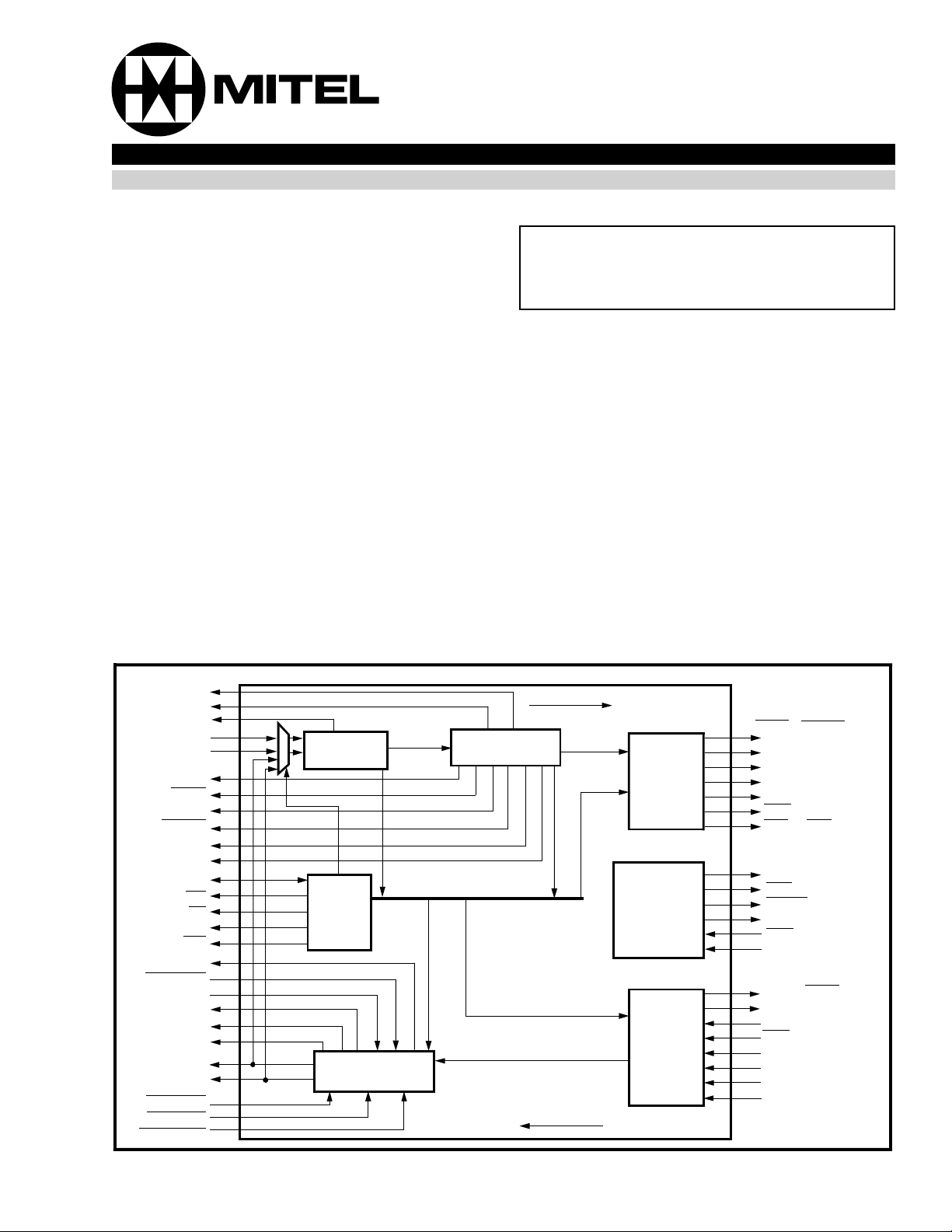
Figure 1 - Functional Block Diagram
5-23
Page 2
MT90733 CMOS Advance Information
ALE
X1
RD
X2
WR
STUFD
STUFC
VDD
AD7
AD6
AD5
AD4
VSS
AD3
AD2
AD1
AD0
OENA
SEL
TEST
VSS
D3RC
VDD
D3TD
XFNO
D3TC
CXCK
VSS
XNC
CXF
CXDCC
10
9
8
7
6
5
4
3
2
1
6867666564
11
12
13
14
15
16
17
18
19
20
21
22
23
24
25
26
282930313233343536373839404142
27
VSS
RCS/RCN
CRF
CRCK
VDD
CRD
RNIB3
RNIB2
VDD
CXD
D3RD
CRDCC
RCG
RFS/RFN
FORCfEBE
VDD
XCK
61
XNIB0
60
63
62
59
XNIB1
58
XNIB2
57
FORCECP
XDS/XNIB3
56
FORCEPP
55
FORCEOE
54
VSS
53
TCIN
52
VDD
51
XFSI
50
TFIN
49
TCOUT
48
TFOUT
47
TCG
46
TDOUT
45
VSS
43
44
FE
RNIB1
RDS/RNIB0
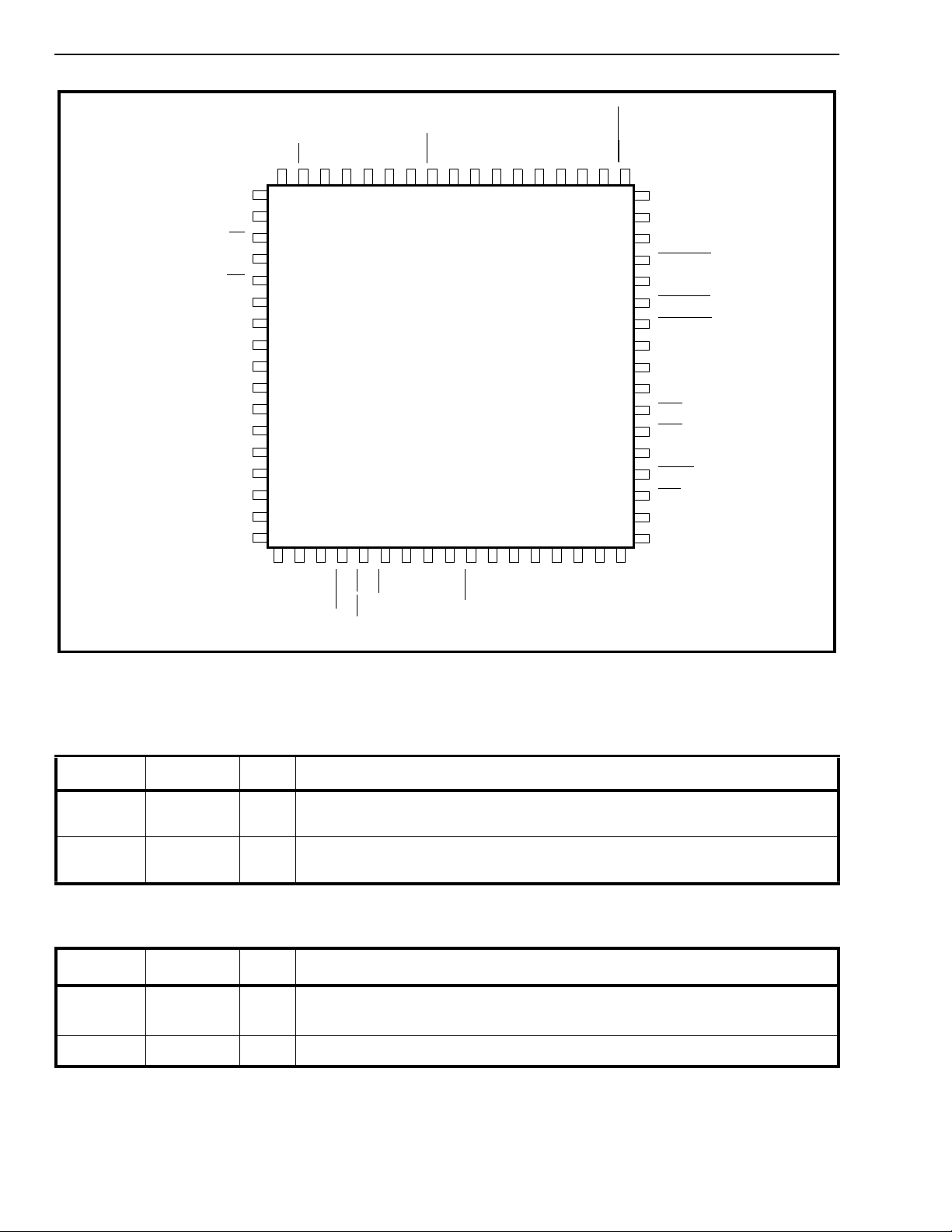
Figure 2 - Pin Connections
Pin Description
Power Supply & Ground
Pin # Name I/O/P Description
4, 17, 27
38, 51, 63
6, 22, 33
44, 53, 67
Note: I = In pu t; O = O u tp ut; P = Po w er
DS3 Receive Line Side Interface
Pin # Name I/O/P Description
5 D3RC I DS3 Receive Cloc k. A 44.736 MHz clock used for clocking in receive data,
29 D3RD I DS3 Receive Data. DS3 line side serial receive data.
Note: I = In pu t; O = O u tp ut; P = Po w er
VDD P Power Supp l y Input. +5v± 5%.
VSS P Ground.
and as the time base for the DS3F receiver.
5-24
Page 3
Advance Information CMOS MT90733
DS3 Transmit Line Side Interface
Pin # Name I/O/P Description
1 D3TC O DS3 Transmit Clock. A 44.736 MHz clock that is derived from the transmit
clock (XCK) signal and is used for clocking out the line side DS3 data signal.
3 D3T D O DS 3 Transmit Data. DS3 line side serial transmit data.
Note: I = In pu t; O = O u tp ut; P = Po w er
Receive Terminal Side Interfac
e
Pin # Name I/O/P Description
31
RFS/RFN O Receive Fram ing Pulse for S eri al/Ni bble In terface. The fram ing pulse is
synchronous with the first bit 1 in the DS3 frame or nibble 1175.
32 RCG
O Receive Clock Gap Signal. The active low gap signal is synchro nous with
each overhead bit in the serial DS3 frame (first bit in the 85-bit group).
34 RCS/RCN O Receive Clock for Serial/Nibble Interface. Clock used for clocking out the
terminal side receive serial and nibble data .
39
40
41
42
Note: I = In pu t; O = O u tp ut; P = Po w er
Transmit Terminal Side Inter fac
RNIB3
RNIB2
RNIB1
RDS/RNIB0
O Receive Nibble/Serial Interface. Nibble data is clocked out on positive transi-
tions of the nibble clock (RCN). Serial data is clocked out on negative transitions of the receive clock (RCS).
e
Pin # Name I/O/P Description
2
XFNO
O Transmit Framing Pulse for Nibble Interface. An active low , one nibble clock
cycle wide (XCN) pulse that occurs during the second nibble time.
50
XFSI
I Transmit Framing Pulse for Serial Interface: A framing pulse input that must
be synchronous with bit 1 in the transmit serial data DS3 frame.
56
58
59
60
XDS/XNIB3
XNIB2
XNIB1
XNIB0
I Transmit Nibble/Serial Interface. Nibble data is clocked in on positive transi-
tions of the nibble clock (XCN). Serial data is clocked into the DS3F on positive transitions of the transmit clock (XCK).
62 XCK I Transmit Clock. A 44.736 Mbit/s cl oc k input with a stabili ty of ±20 ppm and a
duty cycle of 50 ±10%. XCK provides the tim e base for the transm itte r in the
DS3F.
66 XCN O Transmit Clock for Nibble Interface . Output clock signal derived from the
transmit clock (XCK).
Note: I = In pu t; O = O u tp ut; P = Po w er
5-25
Page 4

MT90733 CMOS Advance Information
Transmit Reference Generator Interface
Pin # Name I/O/P Description
45 TDOUT O Transmit Reference Generator Data Output. A DS3 frame is provided on
this signal lead with only the appropriat e M and F bits. A ll other bits in the
frame are held active low.
46 TCG
47 TFO UT
48 TCOUT O Transmit Reference Generator Clock Out. Clock signal that is derive d f rom
52 TCIN I Transmit Reference Generator Clock In. A 44.736 Mbit/s clock with a stabil-
Note: I = In pu t; O = O u tp ut; P = Po w er
Receive C-Bit Interface
Pin # Name I/O/P Description
30 CRDCC
35 C RF O C-Bit Receive F raming Pulse. Provide s a time base ref erence for clocking in
O Transmit Reference Generator Clock Gap Signa l. An active low , one clock
cycle wide (TCOUT) output signal that is synchronous with bit 1 in each 85-bit
group (56 overhead bits) in the DS3 frame.
O Transmit Reference Generator Framing Pulse . An active low, one clock
cycle wide (TCOUT) output pulse that is synch ronous with bit 1 in the DS3
frame.
the transmit reference generator clock input (TCI N).
ity of ±20 ppm and a duty cycle of 50 ±10%.
O C-Bit Receive Data Link Clock. A gapped clock provided for clocking in the
three data link bits (C13, C14, and C15) into external circuit r y from the serial
data (CRD).
the C-bits in a DS3 frame.
36 CRCK
37 CRD O C-Bit Receive Data. Serial int erface f or receiving the selected C -bits in the C-
Note: I = In pu t; O = O u tp ut; P = Po w er
Transmit C-Bit Interface
Pin # Name I/O/P Description
28 CXD I C-Bit Transmit Data. Serial interface for transmitting the selected C-bits in the
64 CXDCC O C-Bit Transmit Data Link Clock. A gapped clock provided for clocking the
65 CXF O C-Bit Transmit Framing Pulse. Identifies the location of the first C-b it in the
68 C XCK O C-Bit Transmit Clock. A gapped clock which clocks the external C-bit serial
Note: I = In pu t; O = O u tp ut; P = Po w er
O C-Bit Receive Clock. A gapped clock which clocks C-bit data out of the DS3F
on positive transitions.
bit parity mode.
C-bit parity mode.
three data link bits (C13, C14, and C15).
DS3 frame.
data into the DS 3F on positive transi tio ns.
5-26
Page 5

Advance Information CMOS MT90733
Other Signals
Pin # Name I/O/P Description
7TESTITest Pin: Leave open.
9OENAOOverhead Enabl e. An active high signal that enables an overhead error to be
introduced into the overhead bit in the next 85th group by placing a low on the
FORCEOE
11 X1 O DS 3 Received X-Bit 1. An output indicat ion of the st at e of the first X-b it
received in the DS3 frame.
13 X2 O DS 3 Recei ved X-Bit 2. An output indication of the stat e of the second X-bit
received in the DS3 frame (bit 680).
15 STUF D O Stuff Data Status. This output signal provides an indication of the state of the
stuff opportunity bit from the received DS3F frame.
16 STUFC O Stuff Clo ck. Provided for clocking out the stuff opportunity bit state.
43 FE O Framing Error Indication. An active high signal is generated when a framing
error is detected while in frame alignment. The framing error indication is held
active low when a DS3 out of frame alarm occurs.
lead.
49 TFI N
54 FORCE O E
I Optional Framing Input Pulse. Not required for normal operation.
I Force DS3 Overhead Bit Error. An active low input signal used in conjunction
with the overhead enable signal (OENA) for introducing an overhead bit error
in the next transmitted 85-bit group.
55 FORCEPP
I Force P-Bit Parity Error. An active low input signal generates and transmits a
P-bit error by inverting both P-bits.
57 FORCECP
I Force C-Bit Parity Error. An active low input signal generates and transmits a
C-bit parity error when operating in the C-bit parity mode.
61 FORCFEBE
I Force FEBE Error. An active low input signal generates and transmits a far
end block error (FEBE) when operating in the C-bit parity mode.
Note: I = In pu t; O = O u tp ut; P = Po w er
Microprocesssor Interface
Pin # Name I/O/P Description
8 SEL
I Microprocessor Select. A low enables the processor to access the DS3F
memory map for control, status and alarm inf ormat ion.
10 ALE I Address Latch Enable. An active high input signal is used by the processor
to hold an address stable during a read/write bus cycle on the falling edge.
12 RD
I Read. An active low input signal generated by the processor for reading the
registers which reside in the DS3F memo ry map.
14 WR
18-21
23-26
Note: I = In pu t; O = O u tp ut; P = Po w er
AD(7-4)
AD(3-0))
I Write. An active low input signal generat ed by the processor for writing to the
I/O Address/Data Bus. These leads constitute the time multiplexed address and
registers which reside in the memory map.
data bus for accessing the registers which reside in the DS3F memory map.
5-27
Page 6

MT90733 CMOS Advance Information
Functional Description
The MT90733 (DS3F) is designed for DS3 framer
applications in which broadband payloads are
mapped into the DS3 frame format. Although the Cbit parity format is recommended, the DS3F can also
operate in the M 13 mode. In the C-bit parity format,
the DS3F provides a separate int erface for selected
C-bits. The DS3F can transmit and receive the
FEAC channel, generate and detect DS3 AIS, DS3
idle, P-bit parity and C-bit parity. In addition,
performance counters are provided, as well as the
ability to generate single framing, FEBE, C-bit parity
and P-bit parity errors. The payload interface is
selectable through software as either a bit serial or
nibble-parallel format. Figure 1 shows the block
diagram for the MT90737 (DS3F).
The DS3F receives a DS3 data signal (D3RD) and a
clock signal (D3RC) from a line interface device. The
DS3 receive block performs DS3 frame alignment,
monitors the signal and the input clock for loss of
signal (LOS), out of frame (OOF), and loss of clock
(LOC). A framing error (FE) output is provided to
indicate when any of the 28 framing bits in the DS3
signal are in error.
(such as the FEAC channel), or provided from the
external C-bit interface.
DS3 loopback is controlled by setting a bit in the
memory map. The entire device is used when
loopback is in affect, but the line side input data and
clock are blocked (by the gate preceding the DS3
Framer Block shown in Figure 1).
The capability to generate and transmit single
overhead bit errors is also provided. External
interfaces are provided for transmitting a far end
block error (FORCFEBE
(FORCEPP
overhead bit error (FORCEOE
signal is used in conjunction with the enable signal
(OENA) for introducing an overhead bit error in the
next 85-bit segment of the DS3 frame.
The Transmit Frame Reference Generator Block
provides reference timing for bit-serial operation.
This block accepts an external 44.736 MHz clock
signal (TCIN) and derives a clock signal (TCOUT), a
framing pulse (TFOUT), a clock gap signal (TCG)
and a data signal (TDOUT). The TDOUT signal
consists of framing b i ts a nd z e ro s elsewhere.
), a C-bit parity error (FORCECP) and an
), a P-bit parity error
). The FORCEOE
The DS3 Interpreter Block performs P-bit and C-bit
parity detection and error counting, receive AIS and
idle pattern detection, far end block error (FEBE)
detection and error counting, far end alarm and
control (FEAC) code word detection, C-bit reception,
and X-bit reception. Serial interfaces are provided for
the received X-bits and for 14 of the 21 C-bits. The
clock s ignal (CR CK
for clocking out C-bits C2, C3 through C6, and C13
through C21. The data communication link clock
(CRDCC
C15, which are assigned as a data communication
channel. An interface that indicates the state of the
stuff opportunity bit (STUFD) during each of the
seven DS3 subframes and a clock signal (STUFC) is
also provided.
The Output Block provides a bit-serial or a nibbleparallel interface. The interface is selected by writing
a control bit in the memory map, and is common to
the DS3F receive and transmit circuitry.
In the transmit direction, the Input Block provides
either a serial or parallel interface. The DS3 Send
Block performs P-bit and C-bit parity generation, AIS
and idle pattern generation, far end alarm and
control (FEAC) transmission, X-bit insertion, and Cbit insertion. The C-bits may be generated internally
(such as C-bit parity), written by the microprocessor
) is present only for C-bits C13, C14, and
) is gapped and is available only
The microprocessor bus interface consists of eight
bidirectional data and address leads (AD7-AD0),
along with other microprocessor control leads. The
microprocessor bus is used to write control
information and to read status information and
alarms.
Typical App lications
Figure 3 shows an application of the MT90733 in
wideband data transmission at 44.736Mb/s. The Line
Interface Unit (LIU) interfaces to the line on one side
and to the MT90733 on the other. The MT90733,
with the nibble-parallel interface on the t erminal side,
can provide the payload data without the overhead
information. Similarly, the overhead data can be
loaded from the terminal side and mapped into DS3
format by the MT90733. The C-bits may be inserted
internally, written by the microprocessor, or
generated by the external C-bit interface.
Figure 4 shows a video application where the
MT90733 is used for the reception of TV signals and
commands transmission. Simple compression
techniques allow the TV signal to be transmitted and
received in DS3 bandwidth. The bandwidt h required
for the command channel in the other direction is
very low.
5-28
Page 7

Advance Information CMOS MT90733
Rx
Line Side
Tx
Rx
Tx
LIU Terminal
MT90733
Figure 3. Wideband Data Transport Using MT90733
Video Signal
TV
MT90733LIU
TerminalLine Side
Codec
Commands
Wideband
Data Sink / Source
TV
Figure 4. Video Application Using MT90733
5-29
Page 8

MT90733 CMOS Advance Information
NOTES:
5-30
 Loading...