

Page 1
CMOS
MT90732
E2/E3 Framer (E2/E3F)
Advance Information
Features
• Framer for CCITT Recommendations
- G.742 (8448 kbit/s)
- G.745 (8448 kbit/s)
- G.751 (34368 kbit/s)
- G.753 (34368 kbit/s)
• Line side interfac e
- Dual rail or NRZ
• HDB3 code c for dual rail I/O
• Terminal side interface
- Nibble-parallel
- Bit-serial
• Transmit reference generator for bit-serial I/O
• Microprocesso r or control leads
• I/O port for servic e bits
Applications
• Line term inals
• Wideban d dat a or vide o tran spor t
• Test e quipm ent
• Multiplexer systems
ISSUE 1 May 1995
Ordering Information
MT90732AP 68 Pin PLCC
-40°C to +85°C
Description
The MT90732 E2/E3 Framer (E2/E3F) is a CMOS
VLSI device that provides the functions needed to
frame a wideband payload to one of four CCITT
Recommendations. G. 742, G.745, G.751, or G.753.
The E2/E3 Framer interfaces to line circuitry with
either dual rail or NRZ signals. On the terminal side,
the interface can be either nibble-parallel or bitserial.
The MT90732 can be operated with or without a
microprocessor. When interfaced with a
microprocessor, the E2/E3 Framer provides an 8byte memory map for control, performance counters
and alarm st atus. The MT90732 provides a transmit
and receive interface port for accessing the
overhead bits from each of the four
recommendations. The overhead bits can also be
accessed by the microprocessor via the memory
map.
RDL
RCKL
RP/RDL
RN
RCK/RCKL
CV
RAIS
RLOC
BIP-4E
RLOF
ROD
ROC
ROF
FE
NRZ LINE
BIP-4
M0
M1
MICRO
SER
DAIS
TLBK
PLBK
TAIS
LPT
TLCINV
TLOC
FORCEFE
TOD
TOC
TOF
RESET
TP/TDL
TCK/TCKL
Line Side Terminal Side
U.S. Patent Number 5040170
TN
TCKL
TDL
Line
Decoder
Control
Line
Encoder
Data
Clock
Data
Clock
Framer
G.7XX
Send
Data
Clock
Frame
Clock
Data
Framing
Interpreter
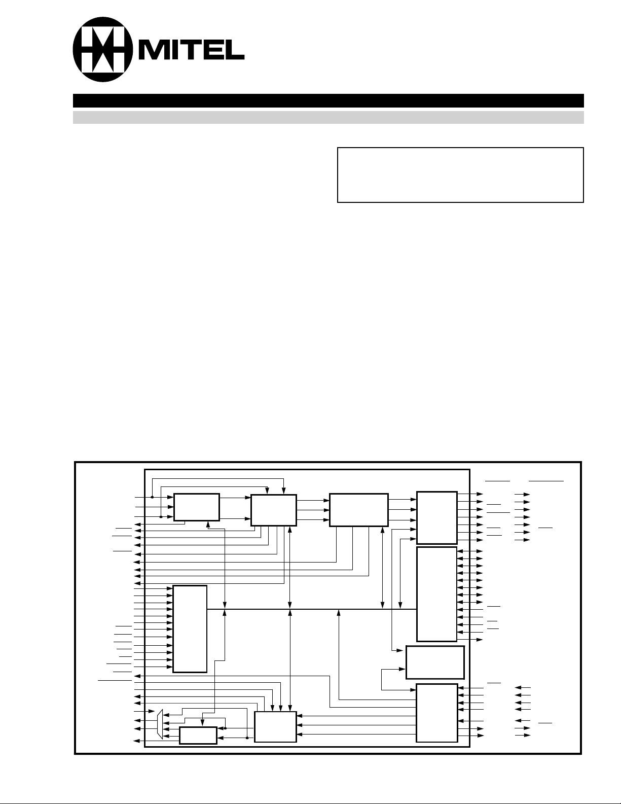
Figure 1 - Functiona l Block Diagram
Data
Clock
Frame
Output
Micro-
processor
I/O
Transmit
Reference
Generator
Input
SERIAL
RSD
TDOUT
TCG
TFOUT
RSC
RSF
RCG N.C.
AD7
AD6
AD5
AD4
AD3
AD2
AD1
AD0
SEL
ALE
RD
WR
RDY
XSF
N.C.
TCIN
XSD
XCK
N.C.
TCOUT
P ARALLEL
RNIB3
RNIB2
RNIB1
RNIB0
RNC
RNF
XNIB3
XNIB2
XNIB1
XNIB0
XCK
XNF
XNC
5-15
Page 2
MT90732 CMOS Advance Information
/RSF
RCG
RNIB3/RSD
RNF
61
BIP-4E
60
59
XNC/TCOUT
58
XNF
57
XCK
56
XNIB0/XSD
55
XNIB1/TCIN
54
XNIB2
53
XNIB3/XSF
GND
52
VDD
51
TLCINV
50
DAIS
49
RDY
48
WR
47
RD
46
ALE
45
SEL
43
44
AD0
AD2
AD1
ROC
ROF
FE
NRZLINE
BIP-4
M0
M1
VDD
GND
MICRO
SER
TLBK
PLBK
TAIS
LPT
TLOC
FORCEFE
ROD
RLOF
RLOC
RAIS
CV
RCK/RCKL
RN
RP/RDL
VDD
GND
RNC/RSC
RNIB0/TFOUT
RNIB1/TCG
RNIB2/TDOUT
10
9
8
7
6
5
4
3
2
1
68676665646362
11
12
13
14
15
16
17
18
19
20
21
22
23
24
25
26
282930313233343536373839404142
27
TOF
TOD
TOC
RESET
TN
TP/TDL
TCK/TCKL
AD7
AD6
AD5
AD4
VDD
GND
AD3
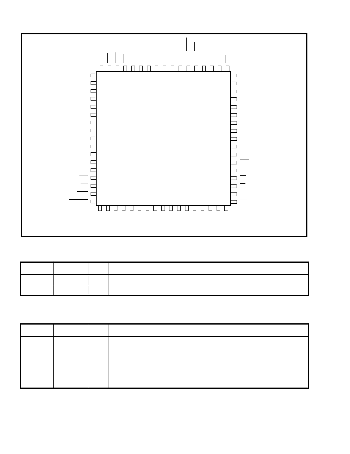
Figure 2 - Pin Connections
Pin Description
Power Supply and Ground
Pin # Name I/O/P Description
1,17,35,51 VDD P VDD. 5-volt supply voltage, +/- 5%
18,34,52,6 8 GND P Ground .
Note: I = Input; O = Output; P = Power
Line Side Receiv e
Pin # Name I/O/P Description
2 RP/RDL I Receive Pos itive Rail /Recei ve NRZ Data. Recei ve positive rail/NRZ dat a
generated from line interface circuit.
3RNIReceive Negative Rail Data. Receive negative rail dat a generat ed from line
interface circuit.
4 RCK/RCKL I Receive Clock Rail/Receive Clock NRZ. The receive clock is used for clock-
ing in the rail/NRZ data signals.
Note: I = Input; O = Output; P = Power
5-16
Page 3
Advance Information CMOS MT90732
Line Side Transmit
Pin # Name I/O/P Description
31 TP/TDL O Transmit Positive Rail/Transmit NRZ Data. Transmit positive rail/NRZ data
sent out of E2/E 3 F ram e r.
32 TCK/TCKL O Transmit Clock Rail/Transmit Clock NR Z. The transm it clo ck is used for
clocking out the dual rail/NRZ data signals. The TCK/TCKL clock signal is
derived from the XCK clock.
33 TN O Transmit Negative Rail Data. Transmit negative rail data sent out of E2/E3
Framer.
Note: I = Input; O = Output; P = Power
T erminal Interface
Pin # Name I/ O/P Description
61 RCG
62 RNF
63 RNIB3/RSD O Receive Nibble Bit 3/Receive Serial Data. Bit 3 is the most significa nt bit in
64 RNIB2/TDOUTO Receive Nibble Bit 2/Transmit Reference Generator Data Outpu t. In t h e
65 RNIB1/TCG
66 RNIB0/T FO
67 RNC/RSC O Receive Nibble Clock/Receive Serial Clock. The nibble and serial clocks are
/RSF O Receive Framing Pulse. Framing pulse is synchronous with the last nibble for
UT
O Receive Clock Gapped. An active low signal indi cates the receive framin g
and service bit locations in the serial mode only.
the nibble-parallel inte rface, and with the first bit in the frame for the bit-serial
interfac e.
the nibble and corresponds to the first bit received in the nibble. The framing
pattern, service bits, and BIP-4 nibble are not provided as parallel dat a. In the
serial mode receive data signal consists of all bits, including the framing pattern and service bits.
nibble-parallel m ode, it is Bit 2 of the received nibble.The reference generat or
is enabled in the serial mode. The output data signal (TDOUT) consists of all
ones in place of the frami ng bits and zeros elsewhere in the f ra me.
O Receive Nibble Bit 1/Transmit Reference Generator Clock Gap Signal. In
the nibble-parallel mod e, it is Bit 1 of the received nibble. The active low TCG
signal indicates the location of the framing pattern and the service b its in the
frame.
O Receive Nibble Bit 0/Transmit Reference Generator Framing Pulse. Bit 0
is the least significant bit in the nibble and is the last bit receive d. The active
low TFOUT
derived from the line side dual rail/N RZ clo ck signal (RCK/RCK L). RNC is
gapped during framing patt ern, service bit and BIP-4 bit times.
signal is synchronous with the first bit in the frame.
53 XNIB3/XSF
54 XNIB2 I Transmit Nibb le Bi t 2. Bit 2 in the 4-bit nibble.
55 XNIB1/TCI
N
I Transmit Nibble Bit 3/Transmit Serial Framing Pu lse. In the nibble-parallel
mode, bit 3 is the most significant bit in the nibble and corresponds to the first
bit transmitted in the nibble. When the terminal interface is serial, the negative
framing pulse is synchronous with the first bit in the frame.
I Transmit Nibble Bit 1/Transmit Reference Generator Clock I n. Bit 1 in the
transmit nibble. For a serial interface, the TCIN is used to derive the clock out
(TCOUT), data signal (TDOUT), framin g pulse (TFO UT
signal (TCG
external payload data into the serial frame.
).The reference generator signals are provided for multiplexing the
), and gapped clock
5-17
Page 4

MT90732 CMOS Advance Information
T erminal Interface
Pin # Name I/ O/P Description
56 XNIB0/XSD I Transmit Nibble Bit 0/Transmit Serial Data. In the nibble-parallel mode, bit 0
is the least significant bit in the nibble. For a serial interface, the input m ust
consist of all the bits in the frame.
57 XCK I Transmit Clock. For the terminal side nibble-parallel inte rface, the XCK is
used for all transmit timing functions, including deriving the nibble output clock
(XNC) and framing pul se (XNF
derived from the transmit reference gene rator clock output (TCOUT ).
).For the serial interface, this clock may be
58 XNF
59 XNC/TCO UTO Transmit Nibble Clock/Transmit Reference Generator Clock Out. The
Note: I = Input; O = Output; P = Power
Service Bit Interface
Pin # Name I/O/P Description
9RODOReceive Service Data Bits . These service bits are clocked out of E2/E3
10 ROC O Receive Service Bits Clock. A gapped clock that clocks out the service bits.
11 ROF O Receive Service Bits Framing Pulse. A positive framing pulse t hat is syn-
27 TOD I Transmit Service Data Bits. The service bits are clocked into E2/E3 Framer
O Transmit Nibble Fram in g P ul s e. The XNF and clock signal (XNC) are pro-
vided for multiplexing nibble data into the E2/E3 Framer from external circuitry.
The negative fram ing pulse identi fies the first bit in the frame.
XNC is derived from the transmit cloc k (XCK) and is used as a time base for
clocking data out of the external multiplexer and into the E2/E3 Framer . XNC is
gapped during the framing pat te rn, service bit and BIP-4 bit times. TCOUT is
derived from the input cloc k (TCIN), and has the same dut y cycle.
Framer on positive transition s of clock signal (ROC).
The clock is active only for clocking out the receive service data bits(ROD).
chronous with the first bit in the frame.
on positive transitions of clock signal (TOC).
28 TOC O Transmit Servi ce Bits Cl ock. A gapped clock that clocks in the service bits.
The clock is active only for clocking in the transmit service data bits (TOD).
29 TOF O Transm i t Service Bits Fr am ing P ulse. A positive framing pulse th at is syn-
chronous with the first bit in the frame.
Note: I = Input; O = Output; P = Power
Microprocessor Interface
Pin # Name I/O/P Description
36-43 AD(7-0) I/ O Address/Data Bus. These leads constitute the time-multiplexed address and
data bus for accessing the registers which reside in the E2/E3F.
44 SEL
45 ALE I Address Latch Enable. An active high signal generat ed by the microproces-
46 RD
5-18
I Select. A low enables the microprocessor to access the E2/E3F memory map
for control, status, and alarm inf ormat ion .
sor. Used by the microprocessor to hold an address stable during a read/write
bus cycle.
I Read. An active low signal generated by the microprocessor for reading the
registers which reside in the memory map.
Page 5

Advance Information CMOS MT90732
Microprocessor Interface
Pin # Name I/O/P Description
47 WR I Write . An active low signal genera ted by the microprocessor f or writing to the
registers which reside in the memory map.
48 RDY O Ready. An active high signal indicating an E2/E3F acknowledgment to the
microprocessor that the addressed memo ry map location ca n complete the
data transfer.
Note: I = Input; O = Output; P = Power
Control Interface
Pin # Name I/O/P Description
13 NRZLINE I Non-Return to Zero Line Selection . A high enables an NRZ line input (RP
and TP), and causes the HDB3 deco der/en coder to be b ypas sed. Whe n low
enables the dual rail interface (RP /RN and TP / TN) and the HDB3
decoder/encoder.
14 BIP-4 I Bit Interleaved Parity - 4. A high enables the B I P -4 function. In the transmit
direction, the BIP-4 is calculat ed for dat a nibble s only, and is sent as the last
nibble in the frame format. In the receive dire ction , the BIP-4 is calculat ed for
the data bits only and compared against the received value which is present in
the last four bits of the frame. An output ind icati on (BI P-4 E) occurs when one
or more columns do not match.
16
15
19 M ICRO I Microprocessor Mode. A high enables the microprocessor interface. When
20 SER I Serial Interface. A high selects the bit-serial interf ace for the terminal side
21 TLBK
22 PLBK
23 TAIS
M1
M0
I Mode Control. The two controls select the operating rate of the E2/E3F
according to the table given below.
M1 M 0 Recommendation Rate (kbit/s)
0 0 G.745 8448
0 1 G.742 8448
1 0 G.753 34368
1 1 G.751 34368
the microprocessor is enabled, the following hardware control leads are disabled. BIP-4, Mode (M0 and M1 ), Serial I/O (SER), and transmit AIS (TAIS
Bits are provided in the memory map for controlling these funct ions.
interface. A low selects the nibble-paral lel int erf ace.
I Terminal Loopback. A low enables a transmit to receive loopback at the line
side.
I Payload Loopback. A low enables a receive to transmit loopback at the termi-
nal side in the serial mode of operation only.
I Transmit Alarm Indi catio n S ig nal. A low causes an all ones signal (AI S) to
be sent in place of a G.7XX frame fo rmat .
).
24
26 FORCEFE
LPT
I Loop Timing. A low enables the loop timing feature. Loop timing disabl es the
transmit clock and enables the receive clock to be used as the transmit clock.
I Force Framing Error. The errored bit is sent into the framing pattern upon the
high-to-low transition of this pin.
5-19
Page 6

MT90732 CMOS Advance Information
Control Interface
Pin # Name I/O/P Description
30 RE SET I Reset. A positive pulse applied to this pin resets the internal counters, logic
circuits, and the performance count ers and control bits in the mem ory map to
zero. The reset pulse is applied after the power becomes stable .
49 DAIS
50 TLCI NV
5CVOCoding Violation. A positive pulse, one clock cycle wide, is generated when
6RAIS
7RLOC
8
12 FE O Framing Error. An active high alarm occurs when one or more framing bits
25 TLOC
60 BIP-4E O BIP-4E. A positive pulse occurs when the comparison between the received
Note: I = Input, O = Output, P = Power
RLOF
I Disable AIS. A low disables the aut oma tic insert ion of AIS into the termi nal
side receive nibble/serial bit stream.
I Transmit Line Clock Invert. A low inverts the out put clock TCK/TCK L when
operating in the dual rail mode.
an illegal coding violation is detected.
OReceive Alarm Indication Signal. An active low alarm occurs within one milli-
second after the E2/E3F detects an all ones condition, including in the presence of a 10
ones in the data field is not mistaken as an AIS.
OReceiv e Loss of Clock. An active low alarm occurs when there are no transi-
tions in the received clock (RCK/RCKL). Recovery occurs on the first clock
transition.
O Receive Loss of Fr am e. An active low alarm oc curs when a valid frame can-
not be detected accordingly to G.7XX recommendatio ns.
are in error.
O Transmit Loss of Clock. An active low alarm occurs when there are no transi-
tions in the transmit clock (TCK). Recovery occurs on the first clock transition.
BIP-4 value and the calculated value does not match in a column.
-3
error rate. An incoming signal with a framing pattern and all
Functional Description
The block diagram for the E2/E3F is shown in Figure
1. The E2/E3F receives NRZ data signal (RDL) and
clock signal (RCKL), or a positive (RP) and negative
(RN) rail signal and clock signal (RCK), from a line
interface circuit. The selection of the line interface,
dual rail or NRZ, is controlled by the external lead
labeled NRZ LINE . Indications of HDB3 coding violation errors are provided on an external signal lead
(CV) as pulses. Coding violation errors are also
counted in an 8-bit saturating count er accessed by the
microprocessor thro ugh the memory map.
The selection of the framing format (G.742, G.745,
G.751 or G.753) is done by external control leads (M1
and M0), or by the microprocessor. The Framer Block
performs frame al ignment and ala rm detection including Loss of Frame (RLOF
detection (RAIS
framing error (FE) output is also provided to indicate
when any of the framing bits in the G. 7XX frame are in
error. The disable AIS (DAIS
E2/E3F to provide receive data on the terminal side
) and BIP-4 detection (BIP-4E). A
), Loss of Clock (RLOC), AIS
) control lead pe rmits the
regardless of frame alignment. The external alarm
indications (latched and unlatched states) are provided
in the memory map, and unlatched alarm indications
are provided at signal leads.
The E2/E3F term inal side o utput block provide s either
a bit-serial or a nibble-paral lel interface. Th e interface
is selected by an external control lead (SER) or by the
microprocessor. The bit-serial interface consists of the
following signals: a data o utput signal (RSD), a clock
output signal (RSC), a receive clock gapped output
signal (RCG
clock gapped signal (RCG
vice bit times. The nibble-parall el interface consists of
data output signal having a nibble format (RNIB3
through RNIB0), a clock output signal (RNC), and a
framing pulse ( RNF
pattern, service bits and BIP-4 nibbl e are not provided
at the interface. The receive nibble clock (RNC) is
gapped during framing p attern, service bit and BIP-4
times.
), and a framing pu lse (RSF). Th e rece ive
) identifies framing and s er-
). In the nibble mode, the framing
5-20
Page 7

Advance Information CMOS MT90732
The transmitter operates independently of the receiver,
unless the loop timing f eature(LPT
the receive clock becomes the transmitted clock. In the
transmit direction, the termin al side bit-serial interface
consists of: data input signal (X SD), a cloc k input signal (XCK), an d a fra mi ng p ulse (X S F
allel interface consists of the following signals: a data
input signal having a nibble format (XNI B3 - XNIB0), a
clock input signal (XCK), a framing output pulse (XNF
and a nibble output clock signal (XNC). The transmit
nibble clock (XNC) is stretched to accommodate the
framing pattern, service bit and BIP-4 times.
MT90372 provides interface to service bits as defined
in G.7XX recommendations.The receive service bit
interface consists of: data output (ROD), clock output
(ROC), and framing pulse (ROF) output. The clock signal (ROC) is gapped and is provided for clocking out
the service bits. The service bit states are also written
into E2/E3F memory locations, which ca n be read by
the microprocessor. The transmitted service bits are
inserted into the frame format from either an external
interface or from memory m ap locations. The transm it
service bit interface consists of data input signal
(TOD), a clock output (TOC), and a framing pulse
(TOF) output.
To fix transmit time-base for the terminal payload multiplexer circuitry, while operating in the bit-serial mode,
the E2/E3F provides a transmit frame reference generator. The tra nsmit frame reference generat or accepts
an external 8.448 or 34.368 MHz clock signal (TCIN)
and produces a clock out signal (TCOUT), a framing
pulse (TFOUT
signal (TDOUT). The data signal consists of G.7XX
framing bits and zeros elsewhere.
), a clock gap signal (TCG), and a data
) is selected, when
). The nibbl e-par-
also controls the r eceive in terf ace sele ction. W hen the
internal HDB3 Encoder B lock is bypassed, the transmit line interf ace consi sts of a data signal (T DL) an d a
clock signal (TCKL). When the HDB3 encoder is
enabled, the transm it l ine inte rface co n sists of po sitive
(TP) and negative (TN) rail signals and a clock signal
(TCK ).
),
A high placed on the microprocessor control lead
(MICRO) selects the microprocessor interface. All the
external control leads, except the loop timing (LPT
receive AIS disable (DA IS
trol leads (NRZLINE) are disab led when the microprocessor interface is selected.
The microprocessor interfa ce consist s of eight bid ir ectional data and address leads (AD7 - AD0), along with
other microprocessor control leads, including a rea dy
(RDY) signal.
), and the lin e in terf ace con -
Typica l Applicat ion
The E2/E3 Framer is used for wideband data
transport as shown in Figure 2. In the receive
direction, the E2/E3 Framer receives NRZ or dual rail
data from LIU, removes overhead bits and puts out
only the payload of the incoming signal to the
terminal. Overhead bits can be accessed through
microprocessor or by service bit interface. In the
transmit direction, the E2/E3 Framer receives data
generated from Data Source, adds framing pattern
and service bits and sends it out to LIU. The E2/E3
Framer handles wideband data at either 8448 or 34
368 Kb/s, and can optionally perform BIP-4 making
data tran sp o rt more reliable.
),
The selection of the transmit line interface, dual rail or
NRZ, is controlled b y the NRZLI NE control lead, which
Line Side
Rx
Line
Interface
Unit
Tx
Ov er h e ad b i t- I/O
Figure 2. Wideband Data Transport using E2/E3 Fra mer
E2/E3
Framer
Terminal Side
Wideba n d
Data Sin k/ So u rc e
5-21
Page 8

MT90732 CMOS Advance Information
Notes.
5-22
 Loading...