

MT90500
Multi-Channel ATM AAL1 SAR
Features
• AAL1 Segmentation and Reassembly device
compatible with Structured Data Transfer (SDT)
as per ANSI T1.630 and ITU I.363 standards
• Transports 64kbps and N x 64kbps traffic over
ATM AAL1 cells (also over AAL5 or AAL0)
• Simultaneous processing of up to 1024
bidirectional Virtual Circuits
• Flexible aggregation capabilities (Nx64) to
allow any combination of 64 kbps channels
while maintaining frame integrity (DS0
grooming)
• Support for clock recovery - Adaptive Clock
Recovery, Synchronous Residual Time Stamp
(SRTS), or external
• Primary UTOPIA port (Level 1, 25 MHz) for
connection to external PHY devices with data
throughput of up to 155 Mbps
• Secondary UTOPIA port for connection to an
external AAL5 SAR processor, or for chaining
multiple MT90500 devices
• 16-bit microprocessor port, configurable to
Motorola or Intel timing
• TDM bus provides 16 bidirectional serial TDM
DS5171 ISSUE 4 April 1999
Ordering Information
MT90500AL 240 Pin Plastic QFP
-40 to +85 C
streams at 2.048, 4.096, or 8.192 Mbps for up
to 2048 TDM 64 kbps channels
• Compatible with ST-BUS, MVIP, H-MVIP and
SCSA interfaces
• Supports master and slave TDM bus clock
operation
• Loopback function at TDM bus interface
• Local TDM bus provides clocks, input pin and
output pin for 2.048 Mbps operation
• Master clock rate up to 60 MHz
• Dual rails (3.3V for power minimization, 5V for
standard I/O)
• IEEE1149 (JTAG) interface
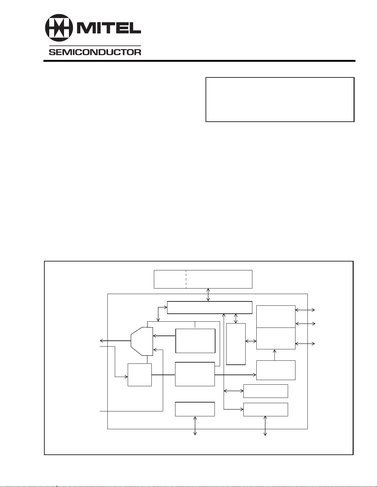
To/From
External
PHY
From
External
ATM SAR
Main
UTOPIA
Interface
Secondary
UTOPIA
Interface
TX
UTOPIA
MUX
RX
UTOPIA
UTOPIA Module
VC
Lookup
Tables
Boundary Scan
Control Structures
and Circular Buffers
External Memory Controller
TX
AAL1
SAR
RX
AAL1
SAR
JTAG
Interface
TX / RX
External
Synchronous
SRAM
TDM Module
TDM Bus
Interface
Internal
TDM
Frame
Buffer
Microprocessor
16-bit Microprocessor Address
and Data Buses
TDM
Clock
Logic
Clock
Recovery
Registers
Interface
TDM Bus
16 Lines
2048 x 64 kbps
(max.)
Local TDM Bus
32 x 64 kbps in
32 x 64 kbps out
Clock Signals
Figure A - MT90500 Block Diagram
1
MT90500
Applications
• B-ISDN (Broadband ISDN) systems requiring
flexible N x 64kbps transport
• Connecting TDM backplane to TDM backplane
over ATM network (GO-MVIP MC4, or other)
• Systems requiring ANSI T1.630 Structured
Data Transfer services for 1 to 122 TDM
channels per VC
• Systems requiring ITU-T I.363.1 circuit
transport over Structured Data Transfer for 1 to
96 TDM channels per VC
• Systems requiring AF-VTOA-0078.000 (ATM
Forum CES v2.0) “Logical Nx64 Basic Service”
• Systems requiring AF-VTOA-0083.000 Voice
and Telephony over ATM (CBR-AAL5).
• Mapping between CBR-AAL0, CBR-AAL5, and
AAL1
• Mapping between CBR partially-filled cells and
full cells
• Mapping between CBR single-voice cells and
Nx64 cells
• ATM uplink for expansion of COs, PBXs, or
open switching platforms using an adjunct ATM
switch
• ATM Public Network access for PBX or CO
• ATM Edge Switches and CPE IntegratedAccess over ATM
• TDM traffic transfer over an asynchronous cell
bus
• Systems requiring Nx64 over CBR-AAL5.
Description
The MT90500 Multi-Channel AAL1 SAR is a highly
integrated solution which allows systems based on a
telecom bus to be interfaced to ATM networks using
ATM Adaptation Layer 1 (AAL1), ATM Adaptation
Layer 5 (AAL5) and ATM Adaptation Layer 0 (AAL0).
The MT90500 can be connected directly to a ST-BUS
time division multiplexed (TDM) backplane
containing up to 1024 full duplex 64kbps channels.
Up to 1024 bi-directional ATM VC connections can
be simultaneously processed by the MT90500 AAL1
SAR device.
On the synchronous TDM bus side, the MT90500
device interfaces with sixteen bidirectional ST-BUS
serial links operating at 2.048, 4.096 or 8.192 Mbps.
TDM bus compatibility with MVIP-90, H-MVIP, and
SCSA interfaces is also provided.
On the ATM interface side, the MT90500 device
meets the ATM Forum standard UTOPIA Bus Level
1. This supports connection to a range of standard
physical layer (PHY) transceivers.
The MT90500 provides a built-in UTOPIA multiplexer
which allows external ATM cells to be multiplexed
with internally-generated cells in the transmit
direction. This feature can be used to connect
another MT90500 (to expand the TDM bandwidth of
the system to 4096 TDM channels), or to connect an
external AAL5 SAR (to multiplex non-CBR ATM cell
traffic with the MT90500 CBR stream).
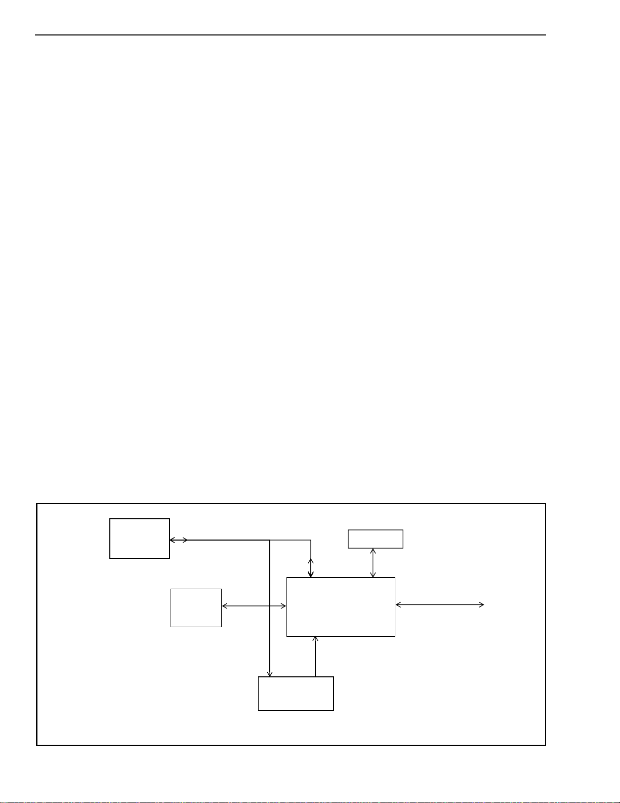
Primary
Off-the-shelf
ATM PHY
Device
16-bit CPU port for
internal register and
external memory programming
CPU
UTOPIA
Port
Off-the-shelf
SAR Device
(AAL5)
Local Memory
MT90500
AAL1 SAR
Secondary
UTOPIA
Port
External
Synchronous
SRAM
TDM Data, Clock
and Sync Lines
MVIP-90
H-MVIP
ST-BUS
SCSA
IDL
Figure B - MT90500 Device Application Block Diagram
2

MT90500
Table of Contents
1. Introduction. . . . . . . . . . . . . . . . . . . . . . . . . . . . . . . . . . . . . . . . . . . . . . . . . . . . . . . . . . . . . . . . . . . . . . . . . . 11
1.1 Functional Overview . . . . . . . . . . . . . . . . . . . . . . . . . . . . . . . . . . . . . . . . . . . . . . . . . . . . . . . . . . . . . . . . 11
1.2 Reference Documents . . . . . . . . . . . . . . . . . . . . . . . . . . . . . . . . . . . . . . . . . . . . . . . . . . . . . . . . . . . . . .12
1.3 ATM Glossary . . . . . . . . . . . . . . . . . . . . . . . . . . . . . . . . . . . . . . . . . . . . . . . . . . . . . . . . . . . . . . . . . . . . . 13
2. Features. . . . . . . . . . . . . . . . . . . . . . . . . . . . . . . . . . . . . . . . . . . . . . . . . . . . . . . . . . . . . . . . . . . . . . . . . . . . . 15
2.1 General . . . . . . . . . . . . . . . . . . . . . . . . . . . . . . . . . . . . . . . . . . . . . . . . . . . . . . . . . . . . . . . . . . . . . . . . . . 15
2.2 Serial TDM Bus. . . . . . . . . . . . . . . . . . . . . . . . . . . . . . . . . . . . . . . . . . . . . . . . . . . . . . . . . . . . . . . . . . . . 15
2.3 CBR ATM Cell Processor . . . . . . . . . . . . . . . . . . . . . . . . . . . . . . . . . . . . . . . . . . . . . . . . . . . . . . . . . . . . 15
2.4 External Memory Interface . . . . . . . . . . . . . . . . . . . . . . . . . . . . . . . . . . . . . . . . . . . . . . . . . . . . . . . . . . . 16
2.5 UTOPIA Interface and Multiplexer . . . . . . . . . . . . . . . . . . . . . . . . . . . . . . . . . . . . . . . . . . . . . . . . . . . . . 16
2.6 Microprocessor Interface. . . . . . . . . . . . . . . . . . . . . . . . . . . . . . . . . . . . . . . . . . . . . . . . . . . . . . . . . . . . . 16
2.7 Miscellaneous . . . . . . . . . . . . . . . . . . . . . . . . . . . . . . . . . . . . . . . . . . . . . . . . . . . . . . . . . . . . . . . . . . . . . 16
2.8 Interrupts. . . . . . . . . . . . . . . . . . . . . . . . . . . . . . . . . . . . . . . . . . . . . . . . . . . . . . . . . . . . . . . . . . . . . . . . . 17
2.8.1 Module Level Interrupts. . . . . . . . . . . . . . . . . . . . . . . . . . . . . . . . . . . . . . . . . . . . . . . . . . . . . . . . . 17
2.8.2 TX_SAR Interrupts . . . . . . . . . . . . . . . . . . . . . . . . . . . . . . . . . . . . . . . . . . . . . . . . . . . . . . . . . . . . 17
2.8.3 RX_SAR Interrupts . . . . . . . . . . . . . . . . . . . . . . . . . . . . . . . . . . . . . . . . . . . . . . . . . . . . . . . . . . . . 17
2.8.4 UTOPIA Interrupts. . . . . . . . . . . . . . . . . . . . . . . . . . . . . . . . . . . . . . . . . . . . . . . . . . . . . . . . . . . . . 17
2.8.5 TDM Interrupts. . . . . . . . . . . . . . . . . . . . . . . . . . . . . . . . . . . . . . . . . . . . . . . . . . . . . . . . . . . . . . . . 17
2.8.6 Timing Module Interrupts. . . . . . . . . . . . . . . . . . . . . . . . . . . . . . . . . . . . . . . . . . . . . . . . . . . . . . . . 18
2.9 Statistics . . . . . . . . . . . . . . . . . . . . . . . . . . . . . . . . . . . . . . . . . . . . . . . . . . . . . . . . . . . . . . . . . . . . . . . . . 18
2.9.1 RX_SAR Statistics. . . . . . . . . . . . . . . . . . . . . . . . . . . . . . . . . . . . . . . . . . . . . . . . . . . . . . . . . . . . . 18
2.9.2 TDM Statistics . . . . . . . . . . . . . . . . . . . . . . . . . . . . . . . . . . . . . . . . . . . . . . . . . . . . . . . . . . . . . . . . 18
2.9.3 Timing Recovery Statistics . . . . . . . . . . . . . . . . . . . . . . . . . . . . . . . . . . . . . . . . . . . . . . . . . . . . . . 18
3. Pin Descriptions . . . . . . . . . . . . . . . . . . . . . . . . . . . . . . . . . . . . . . . . . . . . . . . . . . . . . . . . . . . . . . . . . . . . . . 19
4. Functional Description. . . . . . . . . . . . . . . . . . . . . . . . . . . . . . . . . . . . . . . . . . . . . . . . . . . . . . . . . . . . . . . . . 28
4.1 TDM Module . . . . . . . . . . . . . . . . . . . . . . . . . . . . . . . . . . . . . . . . . . . . . . . . . . . . . . . . . . . . . . . . . . . . . . 28
4.1.1 TDM Clock Logic . . . . . . . . . . . . . . . . . . . . . . . . . . . . . . . . . . . . . . . . . . . . . . . . . . . . . . . . . . . . . . 28
4.1.1.1 TDM Timing Modes . . . . . . . . . . . . . . . . . . . . . . . . . . . . . . . . . . . . . . . . . . . . . . . . . . . . . . . 28
4.1.1.2 REF8KCLK Selection Logic. . . . . . . . . . . . . . . . . . . . . . . . . . . . . . . . . . . . . . . . . . . . . . . . .30
4.1.1.3 Main TDM Bus Timing and Clock Generation Logic . . . . . . . . . . . . . . . . . . . . . . . . . . . . . . 31
4.1.1.4 TDM Clock Drivers. . . . . . . . . . . . . . . . . . . . . . . . . . . . . . . . . . . . . . . . . . . . . . . . . . . . . . . . 31
4.1.1.5 Clock Failure Detection . . . . . . . . . . . . . . . . . . . . . . . . . . . . . . . . . . . . . . . . . . . . . . . . . . . . 31
4.1.2 TDM Interface Operation. . . . . . . . . . . . . . . . . . . . . . . . . . . . . . . . . . . . . . . . . . . . . . . . . . . . . . . . 32
4.1.2.1 Main TDM Bus Operation. . . . . . . . . . . . . . . . . . . . . . . . . . . . . . . . . . . . . . . . . . . . . . . . . . . 32
4.1.2.2 TDM Loopback. . . . . . . . . . . . . . . . . . . . . . . . . . . . . . . . . . . . . . . . . . . . . . . . . . . . . . . . . . . 32
4.1.2.3 Per-channel Output Enable Feature . . . . . . . . . . . . . . . . . . . . . . . . . . . . . . . . . . . . . . . . . . 32
4.1.2.4 Local Bus Operation. . . . . . . . . . . . . . . . . . . . . . . . . . . . . . . . . . . . . . . . . . . . . . . . . . . . . . . 32
4.1.2.5 Local Bus Data Transfer Process . . . . . . . . . . . . . . . . . . . . . . . . . . . . . . . . . . . . . . . . . . . . 33
4.1.3 TDM Data to External Memory Process . . . . . . . . . . . . . . . . . . . . . . . . . . . . . . . . . . . . . . . . . . . .33
4.1.3.1 General . . . . . . . . . . . . . . . . . . . . . . . . . . . . . . . . . . . . . . . . . . . . . . . . . . . . . . . . . . . . . . . . 33
4.1.3.2 Transmit Circular Buffer Control Structures. . . . . . . . . . . . . . . . . . . . . . . . . . . . . . . . . . . . . 34
4.1.3.3 Transmit Circular Buffers . . . . . . . . . . . . . . . . . . . . . . . . . . . . . . . . . . . . . . . . . . . . . . . . . . . 35
4.1.4 External Memory to TDM Data Output Process . . . . . . . . . . . . . . . . . . . . . . . . . . . . . . . . . . . . . . 35
4.1.4.1 General . . . . . . . . . . . . . . . . . . . . . . . . . . . . . . . . . . . . . . . . . . . . . . . . . . . . . . . . . . . . . . . . 35
4.1.4.2 External Memory to Internal Memory Control Structures. . . . . . . . . . . . . . . . . . . . . . . . . . . 36
4.2 External Memory Controller . . . . . . . . . . . . . . . . . . . . . . . . . . . . . . . . . . . . . . . . . . . . . . . . . . . . . . . . . . 38
4.3 TX_SAR Module . . . . . . . . . . . . . . . . . . . . . . . . . . . . . . . . . . . . . . . . . . . . . . . . . . . . . . . . . . . . . . . . . . . 42
4.3.1 TX_SAR Overview. . . . . . . . . . . . . . . . . . . . . . . . . . . . . . . . . . . . . . . . . . . . . . . . . . . . . . . . . . . . . 42
4.3.1.1 General . . . . . . . . . . . . . . . . . . . . . . . . . . . . . . . . . . . . . . . . . . . . . . . . . . . . . . . . . . . . . . . . 42
4.3.1.2 Supported ATM Cell Formats. . . . . . . . . . . . . . . . . . . . . . . . . . . . . . . . . . . . . . . . . . . . . . . .42
4.3.1.3 Transmit Event Scheduler Overview . . . . . . . . . . . . . . . . . . . . . . . . . . . . . . . . . . . . . . . . . . 45
4.3.1.3.1 Introduction. . . . . . . . . . . . . . . . . . . . . . . . . . . . . . . . . . . . . . . . . . . . . . . . . . . . . . . . . 45
4.3.1.3.2 Fixed TDM Payload Schedulers. . . . . . . . . . . . . . . . . . . . . . . . . . . . . . . . . . . . . . . . . 45
4.3.1.3.3 AAL1 Long/Short Schedulers . . . . . . . . . . . . . . . . . . . . . . . . . . . . . . . . . . . . . . . . . . . 46
4.3.1.3.4 Other Considerations . . . . . . . . . . . . . . . . . . . . . . . . . . . . . . . . . . . . . . . . . . . . . . . . .47
3

MT90500
4.3.2 TX_SAR Process . . . . . . . . . . . . . . . . . . . . . . . . . . . . . . . . . . . . . . . . . . . . . . . . . . . . . . . . . . . . . .48
4.3.2.1 Transmit Event Schedulers. . . . . . . . . . . . . . . . . . . . . . . . . . . . . . . . . . . . . . . . . . . . . . . . . .48
4.3.2.2 Transmit Control Structures . . . . . . . . . . . . . . . . . . . . . . . . . . . . . . . . . . . . . . . . . . . . . . . . .50
4.3.3 Non-CBR Data Cell Transmission Capability. . . . . . . . . . . . . . . . . . . . . . . . . . . . . . . . . . . . . . . . .55
4.4 The RX_SAR Module. . . . . . . . . . . . . . . . . . . . . . . . . . . . . . . . . . . . . . . . . . . . . . . . . . . . . . . . . . . . . . . .57
4.4.1 RX_SAR Overview. . . . . . . . . . . . . . . . . . . . . . . . . . . . . . . . . . . . . . . . . . . . . . . . . . . . . . . . . . . . .57
4.4.2 RX_SAR Process. . . . . . . . . . . . . . . . . . . . . . . . . . . . . . . . . . . . . . . . . . . . . . . . . . . . . . . . . . . . . .57
4.4.2.1 RX_SAR Control Structures . . . . . . . . . . . . . . . . . . . . . . . . . . . . . . . . . . . . . . . . . . . . . . . . .58
4.4.2.2 RX_SAR Error Counter and Interrupt Sources . . . . . . . . . . . . . . . . . . . . . . . . . . . . . . . . . . .59
4.4.2.3 Receive Overruns and Underruns. . . . . . . . . . . . . . . . . . . . . . . . . . . . . . . . . . . . . . . . . . . . .60
4.4.2.4 Lost Cell Handling. . . . . . . . . . . . . . . . . . . . . . . . . . . . . . . . . . . . . . . . . . . . . . . . . . . . . . . . .61
4.5 UTOPIA Module. . . . . . . . . . . . . . . . . . . . . . . . . . . . . . . . . . . . . . . . . . . . . . . . . . . . . . . . . . . . . . . . . . . .62
4.5.1 UTOPIA Overview . . . . . . . . . . . . . . . . . . . . . . . . . . . . . . . . . . . . . . . . . . . . . . . . . . . . . . . . . . . . .62
4.5.2 Cell Transmission and Mux Process . . . . . . . . . . . . . . . . . . . . . . . . . . . . . . . . . . . . . . . . . . . . . . .63
4.5.3 Receive Cell Selection Process . . . . . . . . . . . . . . . . . . . . . . . . . . . . . . . . . . . . . . . . . . . . . . . . . . .63
4.5.4 Non-CBR Data Cell Reception Ability. . . . . . . . . . . . . . . . . . . . . . . . . . . . . . . . . . . . . . . . . . . . . . .67
4.6 Clock Recovery from ATM Link . . . . . . . . . . . . . . . . . . . . . . . . . . . . . . . . . . . . . . . . . . . . . . . . . . . . . . . .70
4.6.1 Adaptive Clock Recovery Sub-Module. . . . . . . . . . . . . . . . . . . . . . . . . . . . . . . . . . . . . . . . . . . . . .70
4.6.2 SRTS Clock Recovery Description. . . . . . . . . . . . . . . . . . . . . . . . . . . . . . . . . . . . . . . . . . . . . . . . .72
4.6.2.1 Transmit SRTS Operation. . . . . . . . . . . . . . . . . . . . . . . . . . . . . . . . . . . . . . . . . . . . . . . . . . .72
4.6.2.2 Receive SRTS Operation . . . . . . . . . . . . . . . . . . . . . . . . . . . . . . . . . . . . . . . . . . . . . . . . . . .74
4.7 Microprocessor Interface . . . . . . . . . . . . . . . . . . . . . . . . . . . . . . . . . . . . . . . . . . . . . . . . . . . . . . . . . . . . .77
4.7.1 General. . . . . . . . . . . . . . . . . . . . . . . . . . . . . . . . . . . . . . . . . . . . . . . . . . . . . . . . . . . . . . . . . . . . . .77
4.7.2 A Programming Example - How to Set Up a VC . . . . . . . . . . . . . . . . . . . . . . . . . . . . . . . . . . . . . .77
4.7.3 Microprocessor Access and Device Reset. . . . . . . . . . . . . . . . . . . . . . . . . . . . . . . . . . . . . . . . . . .78
4.8 Test Interface. . . . . . . . . . . . . . . . . . . . . . . . . . . . . . . . . . . . . . . . . . . . . . . . . . . . . . . . . . . . . . . . . . . . . .78
4.8.1 Test Access Port . . . . . . . . . . . . . . . . . . . . . . . . . . . . . . . . . . . . . . . . . . . . . . . . . . . . . . . . . . . . . .78
4.8.2 JTAG ID . . . . . . . . . . . . . . . . . . . . . . . . . . . . . . . . . . . . . . . . . . . . . . . . . . . . . . . . . . . . . . . . . . . . .79
4.8.3 Boundary Scan Instructions . . . . . . . . . . . . . . . . . . . . . . . . . . . . . . . . . . . . . . . . . . . . . . . . . . . . . .79
4.8.4 BSDL . . . . . . . . . . . . . . . . . . . . . . . . . . . . . . . . . . . . . . . . . . . . . . . . . . . . . . . . . . . . . . . . . . . . . . .79
5. Register Map . . . . . . . . . . . . . . . . . . . . . . . . . . . . . . . . . . . . . . . . . . . . . . . . . . . . . . . . . . . . . . . . . . . . . . . . .80
5.1 Register Overview . . . . . . . . . . . . . . . . . . . . . . . . . . . . . . . . . . . . . . . . . . . . . . . . . . . . . . . . . . . . . . . . . .80
5.1.1 General. . . . . . . . . . . . . . . . . . . . . . . . . . . . . . . . . . . . . . . . . . . . . . . . . . . . . . . . . . . . . . . . . . . . . .80
5.1.2 Interrupt Structure. . . . . . . . . . . . . . . . . . . . . . . . . . . . . . . . . . . . . . . . . . . . . . . . . . . . . . . . . . . . . .81
5.1.3 Register Summary . . . . . . . . . . . . . . . . . . . . . . . . . . . . . . . . . . . . . . . . . . . . . . . . . . . . . . . . . . . . .82
5.2 Register Description. . . . . . . . . . . . . . . . . . . . . . . . . . . . . . . . . . . . . . . . . . . . . . . . . . . . . . . . . . . . . . . . .84
5.2.1 Microprocessor Interface Registers . . . . . . . . . . . . . . . . . . . . . . . . . . . . . . . . . . . . . . . . . . . . . . . .84
5.2.2 TX_SAR Registers . . . . . . . . . . . . . . . . . . . . . . . . . . . . . . . . . . . . . . . . . . . . . . . . . . . . . . . . . . . . .87
5.2.3 RX_SAR Registers. . . . . . . . . . . . . . . . . . . . . . . . . . . . . . . . . . . . . . . . . . . . . . . . . . . . . . . . . . . . .91
5.2.4 UTOPIA Registers . . . . . . . . . . . . . . . . . . . . . . . . . . . . . . . . . . . . . . . . . . . . . . . . . . . . . . . . . . . . .94
5.2.5 TDM Interface and Clock Interface Registers. . . . . . . . . . . . . . . . . . . . . . . . . . . . . . . . . . . . . . . . .98
5.2.6 TDM Time Slot Control. . . . . . . . . . . . . . . . . . . . . . . . . . . . . . . . . . . . . . . . . . . . . . . . . . . . . . . . .111
6. Electrical Specification. . . . . . . . . . . . . . . . . . . . . . . . . . . . . . . . . . . . . . . . . . . . . . . . . . . . . . . . . . . . . . . .112
6.1 DC Characteristics. . . . . . . . . . . . . . . . . . . . . . . . . . . . . . . . . . . . . . . . . . . . . . . . . . . . . . . . . . . . . . . . .112
6.2 AC Characteristics . . . . . . . . . . . . . . . . . . . . . . . . . . . . . . . . . . . . . . . . . . . . . . . . . . . . . . . . . . . . . . . . .114
6.2.1 Main TDM Bus . . . . . . . . . . . . . . . . . . . . . . . . . . . . . . . . . . . . . . . . . . . . . . . . . . . . . . . . . . . . . . .114
6.2.2 Local TDM Bus. . . . . . . . . . . . . . . . . . . . . . . . . . . . . . . . . . . . . . . . . . . . . . . . . . . . . . . . . . . . . . .120
6.2.3 CPU Interface - Accessing Registers and External Memory . . . . . . . . . . . . . . . . . . . . . . . . . . . .124
6.2.4 Interface with External Memory . . . . . . . . . . . . . . . . . . . . . . . . . . . . . . . . . . . . . . . . . . . . . . . . . .128
6.2.5 UTOPIA Interfaces . . . . . . . . . . . . . . . . . . . . . . . . . . . . . . . . . . . . . . . . . . . . . . . . . . . . . . . . . . . .131
6.2.5.1 Primary UTOPIA Interface . . . . . . . . . . . . . . . . . . . . . . . . . . . . . . . . . . . . . . . . . . . . . . . . .131
6.2.5.2 Secondary UTOPIA Interface . . . . . . . . . . . . . . . . . . . . . . . . . . . . . . . . . . . . . . . . . . . . . . .133
6.2.6 SRTS User Interface . . . . . . . . . . . . . . . . . . . . . . . . . . . . . . . . . . . . . . . . . . . . . . . . . . . . . . . . . .134
6.2.7 Message Channel Interface . . . . . . . . . . . . . . . . . . . . . . . . . . . . . . . . . . . . . . . . . . . . . . . . . . . . .134
6.2.8 Boundary-Scan Test Access Interface. . . . . . . . . . . . . . . . . . . . . . . . . . . . . . . . . . . . . . . . . . . . .136
7. Applications. . . . . . . . . . . . . . . . . . . . . . . . . . . . . . . . . . . . . . . . . . . . . . . . . . . . . . . . . . . . . . . . . . . . . . . . .137
7.1 Board Level Applications . . . . . . . . . . . . . . . . . . . . . . . . . . . . . . . . . . . . . . . . . . . . . . . . . . . . . . . . . . . .137
4

MT90500
7.2 System Level Applications . . . . . . . . . . . . . . . . . . . . . . . . . . . . . . . . . . . . . . . . . . . . . . . . . . . . . . . . . . 141
7.3 TDM Clock Recovery Applications . . . . . . . . . . . . . . . . . . . . . . . . . . . . . . . . . . . . . . . . . . . . . . . . . . . . 145
7.3.1 General . . . . . . . . . . . . . . . . . . . . . . . . . . . . . . . . . . . . . . . . . . . . . . . . . . . . . . . . . . . . . . . . . . . . 145
7.3.2 SRTS Clock Recovery Considerations . . . . . . . . . . . . . . . . . . . . . . . . . . . . . . . . . . . . . . . . . . . . 145
7.3.3 Free-running Clocks . . . . . . . . . . . . . . . . . . . . . . . . . . . . . . . . . . . . . . . . . . . . . . . . . . . . . . . . . . 146
7.4 External Memory Space and Bandwidth Calculations . . . . . . . . . . . . . . . . . . . . . . . . . . . . . . . . . . . . . 147
7.4.1 External Memory Space Requirements. . . . . . . . . . . . . . . . . . . . . . . . . . . . . . . . . . . . . . . . . . . . 147
7.4.2 Memory Structure Summary . . . . . . . . . . . . . . . . . . . . . . . . . . . . . . . . . . . . . . . . . . . . . . . . . . . . 149
7.4.3 External Memory Bandwidth Requirements . . . . . . . . . . . . . . . . . . . . . . . . . . . . . . . . . . . . . . . . 151
7.5 CBR Throughput Delay. . . . . . . . . . . . . . . . . . . . . . . . . . . . . . . . . . . . . . . . . . . . . . . . . . . . . . . . . . . . . 153
7.6 Other Applications. . . . . . . . . . . . . . . . . . . . . . . . . . . . . . . . . . . . . . . . . . . . . . . . . . . . . . . . . . . . . . . . .154
7.6.1 Payload Switching . . . . . . . . . . . . . . . . . . . . . . . . . . . . . . . . . . . . . . . . . . . . . . . . . . . . . . . . . . . . 154
7.6.2 TDM Switching and Loopback. . . . . . . . . . . . . . . . . . . . . . . . . . . . . . . . . . . . . . . . . . . . . . . . . . . 154
7.6.3 DS0 Trunking, or Dynamic TDM channel re-mapping. . . . . . . . . . . . . . . . . . . . . . . . . . . . . . . . . 155
7.6.4 SCSA Message Channel. . . . . . . . . . . . . . . . . . . . . . . . . . . . . . . . . . . . . . . . . . . . . . . . . . . . . . . 156
8. Physical Specification . . . . . . . . . . . . . . . . . . . . . . . . . . . . . . . . . . . . . . . . . . . . . . . . . . . . . . . . . . . . . . . . 157
5

MT90500
List of Figures
Figure 1 - MT90500 Block Diagram...................................................................................................................12
Figure 2. Pin Connections................................................................................................................................26
Figure 3 - TDM Clock Selection and Generation Logic.....................................................................................29
Figure 4 - TDM Frame Buffer to External Memory Transfer..............................................................................33
Figure 5 - Transmit Circular Buffer Control Structure........................................................................................34
Figure 6 - External Memory to TDM Frame Buffer Transfer..............................................................................35
Figure 7 - External Memory to Internal Memory Control Structure....................................................................37
Figure 8 - Memory Read Pipeline Length..........................................................................................................38
Figure 9 - Logical Byte Address vs. Physical Address and Memory Banks......................................................39
Figure 10 - Read / Write Turnaround Cycles.......................................................................................................40
Figure 11 - Read / Read Turnaround Cycles.......................................................................................................41
Figure 11 - Read / Write turnaround Cycles........................................................................................................41
Figure 12 - AAL1 ATM Cell Format.....................................................................................................................42
Figure 13 - Partially-Filled AAL1 and CBR-AAL0 Cell Formats...........................................................................43
Figure 14 - CBR-AAL5 Cell Format....................................................................................................................44
Figure 15 - Transmit Event Scheduler.................................................................................................................49
Figure 17 - Transmit Control Structure Format (CBR-AAL5)...............................................................................50
Figure 16 - Transmit Control Structure Format (AAL1 & CBR-AAL0) .................................................................51
Figure 18 - a: Sample Three-Channel Transmit Control Structure (AAL1/CBR-AAL0).......................................53
Figure 18 - b: Sample One-Channel Transmit Control Structure (CBR-AAL5) ...................................................53
Figure 19 - Overview of CBR Data Transmission Process..................................................................................54
Figure 20 - VC Pointer For Scheduler-Controlled Non-CBR Data Cell ...............................................................55
Figure 21 - Transmit Non-CBR Data Cell Structure Format................................................................................56
Figure 22 - RX_SAR Control Structure................................................................................................................58
Figure 23 - Overrun and Underrun Situations.....................................................................................................60
Figure 24 - MT90500 Daisy Chain Example........................................................................................................62
Figure 25 - Mux and Internal FIFO Sub-Module Block Diagram .........................................................................63
Figure 26 - Receive Cell Selection Process........................................................................................................65
Figure 27 - MT90500 Cell Receive Process........................................................................................................66
Figure 28 - Look-up Table Non-CBR Data Entry.................................................................................................67
Figure 29 - Received Non-CBR Data Cell Internal Format..................................................................................68
Figure 30 - Overview of CBR Data Reception Process.......................................................................................69
Figure 31 - Adaptive Clock Recovery Sub-Module (Simplified Functional Block Diagram).................................70
Figure 32 - Timing Reference Cell Processing State Machine............................................................................71
Figure 33 - Transmit SRTS Operation.................................................................................................................73
Figure 34 - Receive SRTS Operation..................................................................................................................74
Figure 35 - Clock Recovery Using SRTS Method (Hardware)............................................................................75
Figure 36 - Clock Recovery Using SRTS Method (CPU)....................................................................................76
Figure 37 - A Typical JTAG Test Connection......................................................................................................79
Figure 38. MT90500 Interrupt Structure.............................................................................................................81
Figure 39 - Nominal TDM Bus Timing...............................................................................................................114
Figure 40 - Main TDM Bus Output Clocking Parameters - Positive Frame Pulse.............................................115
Figure 41 - Main TDM Bus Output Clocking Parameters - Negative Frame Pulse ...........................................115
Figure 42 - Main TDM Bus - Serial Output Timing............................................................................................116
Figure 43 - Main TDM Bus - 2/4 Sampling........................................................................................................118
Figure 44 - Main TDM Bus - 3/4 Sampling........................................................................................................118
Figure 45 - Main TDM Bus - 4/4 Sampling........................................................................................................119
Figure 46 - Local TDM Bus Output Parameters - Positive Frame Pulse...........................................................121
6

MT90500
Figure 47 - Local TDM Bus Output Parameters - Negative Frame Pulse ........................................................ 121
Figure 48 - Local TDM Bus - Positive Frame Pulse, 2/4 Sampling .................................................................. 122
Figure 49 - Local TDM Bus - Negative Frame Pulse, 3/4 Sampling................................................................. 123
Figure 50 - Local TDM Bus - Negative Frame Pulse, 4/4 Sampling................................................................. 123
Figure 51 - Intel CPU Interface Timing - Read Access..................................................................................... 124
Figure 52 - Intel CPU Interface Timing - Write Access..................................................................................... 125
Figure 53 - Motorola CPU Interface Timing - Read Access ............................................................................. 126
Figure 54 - Motorola CPU Interface Timing - Write Access.............................................................................. 127
Figure 55 - External Memory Interface Timing - Read Cycle ........................................................................... 129
Figure 56 - External Memory Interface Timing - Write Cycle............................................................................ 130
Figure 57 - Primary UTOPIA Bus - Transmit Timing........................................................................................ 131
Figure 58 - Primary UTOPIA Bus - Receive Timing......................................................................................... 132
Figure 59 - Secondary UTOPIA Interface......................................................................................................... 133
Figure 60 - SRTS User Interface Timing.......................................................................................................... 134
Figure 61 - Message Channel Timing .............................................................................................................. 135
Figure 62 - MT90500 Device Application Block Diagram................................................................................. 137
Figure 63 - UTOPIA Bus Interconnections for Two MT90500s and an AAL5 SAR.......................................... 139
Figure 64 - The MT90500 within a LAN Hub.................................................................................................... 141
Figure 65 - Using the MT90500 with External SAR and ATM Links in a LAN Environment............................. 142
Figure 66 - Access Product using Internal High Speed Cell Bus on the Backplane......................................... 142
Figure 67 - TDM Traffic Transport Over a Cell Bus.......................................................................................... 143
Figure 68 - Connecting CTI Platforms to ATM LANs........................................................................................ 143
Figure 69 - The GO-MVIP, PC-ATM Bus Standard Architecture...................................................................... 144
Figure 70 - SRTS Clocking Application............................................................................................................ 146
Figure 71 - TDM Payload Switching................................................................................................................. 154
Figure 72 - TDM-to-TDM Loopback/Switching................................................................................................. 155
Figure 73 - SCSA Message Bus Application................................................................................................... 156
7

MT90500
List of Tables
Table 1 - Primary UTOPIA Bus Pins................................................................................................................19
Table 2 - Secondary UTOPIA Bus Pins...........................................................................................................20
Table 3 - Microprocessor Bus Interface Pins...................................................................................................20
Table 4 - External Memory Interface Pins........................................................................................................21
Table 5 - Master Clock, Test, and Power Pins.................................................................................................22
Table 6 - TDM Port Pins...................................................................................................................................23
Table 7 - Reset State of I/O and Output Pins...................................................................................................24
Table 8 - Pinout Summary................................................................................................................................25
Table 9 - Memory Size Combinations..............................................................................................................39
Table 10 - Effect of PSEL Field on P-byte Generation.......................................................................................53
Table 11 - Register Summary ............................................................................................................................82
Table 12 - Main Control Register .......................................................................................................................84
Table 13 - Main Status Register.........................................................................................................................84
Table 14 - Window to External Memory Register - CPU....................................................................................85
Table 15 - Read Parity Register.........................................................................................................................85
Table 16 - Memory Configuration Register ........................................................................................................86
Table 17 - TX_SAR Control Register.................................................................................................................87
Table 18 - TX_SAR Status Register...................................................................................................................87
Table 19 - TX_SAR Scheduler Base Register ...................................................................................................88
Table 20 - TX_SAR Frame End Register...........................................................................................................88
Table 21 - TX_SAR End Ratio Register.............................................................................................................88
Table 22 - TX_SAR Control Structure Base Address Register..........................................................................89
Table 23 - Transmit Data Cell FIFO Base Address Register .............................................................................89
Table 24 - Transmit Data Cell FIFO Write Pointer Register...............................................................................89
Table 25 - Transmit Data Cell FIFO Read Pointer Register...............................................................................90
Table 26 - RX_SAR Control Register.................................................................................................................91
Table 27 - RX_SAR Status Register..................................................................................................................92
Table 28 - RX_SAR Misc. Event ID Register.....................................................................................................92
Table 29 - RX_SAR Misc. Event Counter Register............................................................................................92
Table 30 - RX_SAR Underrun Event ID Register...............................................................................................93
Table 31 - RX_SAR Underrun Event Counter Register .....................................................................................93
Table 32 - RX_SAR Overrun Event ID Register.................................................................................................93
Table 33 - RX_SAR Overrun Event Counter Register .......................................................................................93
Table 34 - UTOPIA Control Register..................................................................................................................94
Table 35 - UTOPIA Status Register...................................................................................................................94
Table 36 - VPI / VCI Concatenation Register.....................................................................................................95
Table 37 - VPI Match Register...........................................................................................................................95
Table 38 - VPI Mask Register ............................................................................................................................95
Table 39 - VCI Match Register...........................................................................................................................95
Table 40 - VCI Mask Register............................................................................................................................96
Table 41 - VPI Timing Register..........................................................................................................................96
Table 42 - VCI Timing Register..........................................................................................................................96
Table 43 - Lookup Table Base Address Register...............................................................................................96
Table 44 - Receive Data Cell FIFO Base Address Register ..............................................................................97
Table 45 - Receive Data Cell FIFO Write Pointer Register................................................................................97
Table 46 - Receive Data Cell FIFO Read Pointer Register................................................................................97
Table 47 - TDM Interface Control Register ........................................................................................................98
Table 48 - TDM Interface Status Register..........................................................................................................99
8

MT90500
Table 49 - TDM I/O Register........................................................................................................................... 100
Table 50 - TDM Bus Type Register................................................................................................................. 101
Table 51 - Local Bus Type Register................................................................................................................ 102
Table 52 - TDM Bus to Local Bus Transfer Register....................................................................................... 102
Table 53 - Local Bus to TDM Bus Transfer Register....................................................................................... 103
Table 54 - TX Circular Buffer Control Structure Base Register....................................................................... 103
Table 55 - External to Internal Memory Control Structure Base Register....................................................... 103
Table 56 - TX Circular Buffer Base Address Register..................................................................................... 104
Table 57 - TDM Read Underrun Address Register......................................................................................... 104
Table 58 - TDM Read Underrun Count Register............................................................................................. 104
Table 59 - Clock Module General Control Register......................................................................................... 104
Table 60 - Clock Module General Status Register.......................................................................................... 105
Table 61 - Master Clock Generation Control Register .................................................................................... 106
Table 62 - Master Clock / CLKx2 Division Factor............................................................................................ 107
Table 63 - Timing Reference Processing Control Register............................................................................. 107
Table 64 - Event Count Register..................................................................................................................... 108
Table 65 - CLKx1 Count - Low Register.......................................................................................................... 108
Table 66 - CLKx1 Count - High Register......................................................................................................... 108
Table 67 - DIVX Register ................................................................................................................................ 109
Table 68 - DIVX Ratio Register....................................................................................................................... 109
Table 69 - SRTS Transmit Gapping Divider Register ..................................................................................... 109
Table 70 - SRTS Transmit Byte Counter Register.......................................................................................... 110
Table 71 - SRTS Receive Gapping Divider Register ...................................................................................... 110
Table 72 - SRTS Receive Byte Counter Register........................................................................................... 110
Table 73 - Output Enable Registers................................................................................................................ 111
Table 74 - Absolute Maximum Ratings ........................................................................................................... 112
Table 75 - Recommended Operating Conditions............................................................................................ 112
Table 76 - DC Characteristics......................................................................................................................... 112
Table 77 - Main TDM Bus Output Clock Parameters...................................................................................... 114
Table 78 - Main TDM Bus Data Output Parameters ....................................................................................... 116
Table 79 - Main TDM Bus Input Clock Parameters......................................................................................... 117
Table 80 - Main TDM Bus Input Data Parameters.......................................................................................... 117
Table 81 - Local TDM Bus Clock Parameters................................................................................................. 120
Table 82 - Local TDM Bus Data Output Parameters....................................................................................... 120
Table 83 - Local TDM Bus Data Input Parameters ......................................................................................... 122
Table 84 - Intel Microprocessor Interface Timing - Read Cycle Parameters................................................... 124
Table 85 - Intel Microprocessor Interface Timing - Write Cycle Parameters................................................... 125
Table 86 - Motorola Microprocessor Interface Timing - Read Cycle Parameters ........................................... 126
Table 87 - Motorola Microprocessor Interface Timing - Write Cycle Parameters............................................ 127
Table 88 - MCLK - Master Clock Input Parameters ........................................................................................ 128
Table 89 - External Memory Interface Timing - Clock Parameters ................................................................. 128
Table 90 - External Memory Interface Timing - Read Cycle Parameters........................................................ 128
Table 91 - External Memory Interface Timing - Write Cycle Parameters........................................................ 128
Table 92 - Primary UTOPIA Interface Parameters - Transmit......................................................................... 131
Table 93 - Primary UTOPIA Interface Parameters - Receive.......................................................................... 132
Table 94 - Secondary UTOPIA Parameters Timing........................................................................................ 133
Table 95 - SRTS Interface Parameters........................................................................................................... 134
Table 96 - Message Channel Parameters....................................................................................................... 134
Table 97 - Boundary-Scan Test Access Port Timing ...................................................................................... 136
Table 98 - MT90500 Connections to 18-bit Synchronous SRAM.................................................................... 138
9

MT90500
Table 99 - MT90500 Connections to 32/36-bit Synchronous SRAM................................................................138
Table 100 - MT90500 UTOPIA Signal Directions...............................................................................................140
Table 101 - Recommended TDM Channel Numbers for SRTS VCs .................................................................145
Table 102 - Limits on CDV on Receive SRTS VC..............................................................................................146
Table 103 - Summary of External Memory Structures .......................................................................................149
10

MT90500
1. Introduction
1.1 Functional Overview
The Mitel MT90500 Multi-Channel AAL1 SAR bridges a standard isochronous TDM (Time Division Multiplexed)
backplane to a standard ATM (Asynchronous Transfer Mode) bus. On the TDM bus side, the MT90500 can
interface to 16 bidirectional TDM bus links operating at 2.048, 4.096 or 8.192 Mbps (compatible with MVIP / HMVIP, SCSA and Mitel ST-BUS). On the ATM interface side, the MT90500 provides the UTOPIA bus
standardized by the ATM Forum. The device provides the AAL1 Structured Data Transfer (referred to as SDT
from now on in this document) and pointerless Structured Data Transfer mappings defined by ANSI T1.6301993 and ITU-T I.363. In addition, the MT90500 provides CBR (Constant Bit Rate) mapping of TDM to AAL0,
and to AAL5 (CBR-AAL5). In all data transfer for mats, the user simply ports the T1/E1, T3/E3, etc. traffic onto
the TDM backplane before applying it to the MT90500. As well, the device also suppor ts TDM clock recovery
using adaptive, SRTS, or external clock recovery.
In the receive direction, ATM cells with VCs destined for the MT90500 are extracted from the UTOPIA bus and
sent toward the TDM interface. In the transmit direction, the MT90500 provides multiplexing capabilities at the
UTOPIA interf ace to allo w the use of an external AAL5 SAR device, or multiple MT90500 devices. This is useful
when CBR data and VBR/ABR/UBR data traffic must be transmitted from the local node on the same physical
link. As well, the ability to multiplex internal AAL1 cells with external AAL5 cells can be used to interleave
associated signalling cells and control messages with the AAL1 CBR traffic.
The MT90500 also offers some internal support for non-CBR data traffic. If the application's signalling (nonCBR) data throughput is not high, the MT90500 can transmit and receive AAL5 (or other non-CBR data) to /
from a pair of FIFOs. This requires the microprocessor to perform SAR functions via software, but may remove
the requirement for an external data SAR. Alternatively, if standard AAL5 signalling is not required by the
system, the user can use some TDM channels for HDLC or proprietary signalling.
Segmentation and reassembly of TDM data to / from ATM cells is highly flexible. The MT90500 allows the user
to select one or more TDM channels to be carried on an ATM logical connection with associated VPI/VCI. The
number of TDM channels (1 to 122), the VPI/VCI, the data transfer method (SDT or pointerless Structured Data
Transfer), cell partial-fill level, and the AAL (AAL1, CBR-AAL5, or CBR-AAL0) are all programmable. The time
slot assignment circuit has 64 kbps granularity and allows a group of TDM channels to be carried on a single
ATM logical channel (channel grooming). There is no limitation for distributing n x 64 channels on the TDM bus
(i.e. TDM channels on a given VC can be concatenated or dispersed anywhere on the 16 serial data streams).
Up to 1024 bidirectional virtual circuits (VCs) can be handled simultaneously by the internal AAL1 processors.
At the maximum TDM rate of 8.192 Mbps, up to 2048 input/output 64 kbps channels are available (1024
bidirectional TDM channels). If the ATM VCs are carrying multiple TDM channels (n x 64), less VCs will be
created. The user is given the ability to flexibly define which 64 kbps channels will be converted into ATM VCs.
It should be noted that since the MT90500’s serial TDM port is fully bidirectional, the ATM logical connections
can be defined as full duplex channels (e.g. voice conversation) or one-way connections (e.g. video playback).
Using the full duplex capabilities, up to 1024 simultaneous phone calls could be handled by the MT90500.
The MT90500 allows the user to scale the size of the external synchronous memory to suit the application. The
external memory’s size is influenced by the number of vir tual circuits required, the number of TDM channels
being handled, and the amount of cell delay variation (CDV) tolerance required for the receive VCs. Userdefined lookup tables, data cell FIFOs, and multiple event schedulers also influence the amount of external
memory required.
The MT90500 supports two clocking schemes on the TDM bus: clock master and clock slave. In clock master,
the MT90500 drives the clocks onto the TDM backplane (the TDM clock is recovered from an incoming ATM
VC, or from an external source). In clock slave mode, the MT90500 receives its 8 kHz framing and clocks
(4.096, 8.192 or 16.384 MHz) from the TDM backplane, and times its internal functions from that.
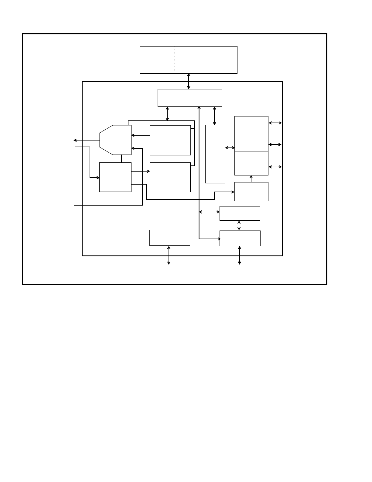
Figure 1 on page 12 shows the MT90500 block diagram. The Applications section of this document illustrates
several connectivity options with external PHY and SAR devices.
11
MT90500
To/From
External
PHY
From
External
SAR
Main
UTOPIA
Interface
Secondary
UTOPIA
Interface
MT90500
TX UTOPIA
MUX
RX
UTOPIA
BLOCK
UTOPIA Module
VC Look-up
Tables
AAL1
SAR
TX / RX Control
Circular Buffers
External Memory
Controller
TX
AAL1
SAR
RX
Structures and
Internal
TDM
Frame
Buffer
External
Synchronous
SRAM
TDM Module
TDM Bus
Interface
Logic
TDM Clock
Logic
Clock
Recovery
Registers
TDM Bus
16 lines
2048 x 64kbps
(max.)
Local TDM Bus
32 x 64 kbps in /
32 x 64 kbps out
Clock
Signals
Boundary-
Scan Logic
JTAG Interface
Microprocessor
Interface Logic
16-bit Microprocessor Interface
Figure 1 - MT90500 Block Diagram
1.2 Reference Documents
MT90500 Programmer’s Manual.
MSAN-171 - TDM Clock Recovery from CBR-over-ATM Links Using the MT90500.
ITU-T Rec. I.363.1, “B-ISDN ATM Adaptation Layer Specification: Type 1 AAL,” 08/1996.
ANSI T1.630, “Broadband ISDN - ATM Adaptation Layer for Constant Bit Rate Services Functionality and
Specification,” 1993.
AF-PHY-0017, “UTOPIA, An ATM-PHY Interface Specification: Level 1, Version 2.01,” March 21, 1994.
AF-VTOA-0078.000, “Circuit Emulation Service Interoperability Specification, Version 2.0,” Jan. 1997.
AF-VTOA-0083.000, “Voice and Telephony Over ATM to the Desktop Specification, Version 2.0,” May 1997.
M. Noorchasm
Forum Contribution 95-1454.
et al.
, “Buffer Design for Constant Bit Rate Services in Presence of Cell Delay Variation,” ATM
Paul E. Fleischer and Chi-Leung Lau, “Synchronous Residual Time Stamp f or Timing Reco very in a Broadband
Network,” United States Patent 5,260,978, Nov. 1993.
IEEE Std. 1149.1a-1993, “IEEE Standard Test Access Port and Boundary Scan Architecture.”
12

1.3 ATM Glossary
MT90500
AAL -
applications into the size and format of an ATM cell.
AAL0 - native ATM cell transmission; proprietary protocol featuring 5-byte header and 48-byte user payload.
AAL1 - ATM Adaptation Layer used for the transport of constant bit rate, time-dependent traffic (e.g. voice,
video); requires transfer of timing infor mation between source and destination; maximum of 47-bytes of user
data permitted in payload as an additional header byte is required to provide sequencing information.
AAL5 - ATM Adaptation Layer usually used for the transport of variable bit rate, delay-tolerant data traffic and
signalling which requires little sequencing or error-detection support.
ANSI T1.630 - American National Standards Institute specification: Broadband ISDN - ATM Adaptation Layer
for Constant Bit Rate Services Functionality and Specification.
Asynchronous - 1. Not synchronous; not periodic. 2. The temporal property of being sourced from
independent timing references. Asynchronous signals have different frequencies, and no fixed phase
relationship. 3. In telecom, data which is not synchronized to the public network clock. 4. The condition or state
when an entity is unable to determine, prior to its occurrence, exactly when an event will transpire.
ATM length cells; asynchronous in the sense that the recurrence of cells containing information from an individual
user is not necessarily periodic. (While ATM cells are transmitted synchronously to maintain clock between
sender and receiver, the sender transmits data cells when it has something to send and transmits empty cells
when idle, and is not limited to transmitting data ever y Nth cell.)
Cell - fixed-size information package consisting of 53 bytes (octets) of data; of these, 5 bytes represent the cell
header and 48 bytes carry the user payload and required overhead.
ATM Adaptation Layer
; standardized protocols used to translate higher layer services from multiple
Asynchronous Transfer Mod
e; a method in which information to be transferred is organized into fixed-
CBR control and strict performance parameters. Used for services such as voice, video, or circuit emulation.
CDV results from buffering and cell scheduling.
CES characteristics of a constant bit rate, dedicated-bandwidth circuit (e.g. T1).
CLP with CLP = 1 can be discarded in a congestion situation.
CSI using SDT, indicates the presence of a pointer byte; used to transport RTS values in odd-numbered cells using
SRTS for clock recovery.
GFC -
default value is “0000”, meaning that GFC protocol is not enforced.
HEC -
check for an error and correct the contents of the header; CRC algorithm allows for single-error correction and
multiple-error detection.
I.363 - ITU-T Recommendation specifying the AALs for B-ISDN (Broadband ISDN).
Isochronous - The temporal property of an event or signal recurring at known periodic time intervals (e.g. 125
µs). Isochronous signals are dependent on some uniform timing, or carry their own timing information
embedded as part of the signal. Examples are DS-1/T1, E1 and TDM in general. From the root words, “iso”
meaning equal, and “chronous” meaning time.
Constant Bit Rate
Cell Delay Variation
Circuit Emulation Service
Cell Loss Priority
; an ATM service category supporting a constant or guaranteed rate, with timing
; a QoS parameter that measures the peak-to-peak cell delay through the network;
; ATM Forum service providing a virtual circuit which emulates the
; a 1-bit field in the ATM cell header that corresponds to the loss priority of a cell; cells
Convergence Sublayer Indication
Generic Flow Control
Header Error Control
; 4-bit field in the ATM header used for local functions (not carried end-to-end);
; using the fifth octet in the ATM cell header, ATM equipment (usually the PHY) may
bit in the AAL1 header byte; when present in an even-numbered cell
OAM bit indicates if the ATM cell carries management information such as fault indications.
Plesiochronous - The temporal property of being arbitrarily close in frequency to some defined precision.
Plesiochronous signals occur at nominally the same rate, any var iation in rate being constrained within specific
limits. Since they are not identical, over the long ter m they will be skewed from each other. This will force a
Operations, Administration and Maintenance
; MSB within the PTI field of the ATM cell header which
13

MT90500
switch to occasionally repeat or delete data in order to handle buffer underflow or overflow. (In
telecommunications, this is known as a frame slip).
PHY physical interfaces that interconnect the various ATM devices.
PTI information or user data; LSB indicates that a AAL5 cell is the final cell in a frame.
QoS VC (e.g cell delay var iation; cell transfer delay, cell loss ratio).
RTS SAR -
reassembling, at the destination, these cells back into infor mation frames; lower sublayer of the AAL which
inserts data from the information frames into cells and then adds the required header, trailer, and/or padding
bytes to create 48-byte payloads to be transmitted to the ATM layer.
SDT -
are segmented into cells for transfer and additional overhead bytes (pointers) are used to indicate structure
boundaries within cells (therefore aiding clock recover y).
SN misinserted ATM cells.
SNP which are designed to provide error-correction on the SN.
SRTS source clock and the network reference clock (time stamps) are transmitted to allow reconstruction of the
source clock. The destination reconstructs the source clock based on the time stamps and the network
reference clock. (Note that the same network reference clock is required at both ends.)
Physical Layer
Payload Type Identifier
Quality of Service
Residual Time Stamp
; bottom layer of the ATM Reference Model; provides ATM cell transmission over the
; 3-bit field in the ATM cell header - MSB indicates if the cell contains OAM
; ATM performance parameters that characterize the transmission quality over a given
; see SRTS.
Segmentation and Reassembly
Structured Data Transfer
Sequence Number
; 4-bit field in the AAL1 header byte used as a sequence counter for detecting lost or
Sequence Number Protection
; format used within AAL1 for blocks consisting of N * 64 kbps channels; blocks
; 4-bit field in the AAL1 header byte consisting of a CRC and a parity bit
Synchronous Residual Time Stamp;
; method of partitioning, at the source, frames into ATM cells and
method for clock recovery in which difference signals between a
SSRAM Synchronous - 1. The temporal property of being sourced from the same timing reference. Synchronous
signals have the same frequency, and a fixed (often implied to be z ero) phase offset. 2. A mode of transmission
in which the sending and receiving terminal equipment are operating continually at the same rate and are
maintained in a desired phase relationship by an appropriate means.
UDT -
structure boundaries (e.g. circuit emulation); term used within ANSI standard - not explicitly stated in ITU.
UTOPIA -
connectivity between ATM components.
VC -
devices; provides sequential, unidirectional transport of ATM cells. Also
VCI -
virtual channel (VC) within a vir tual path (VP) that carr ies a particular cell.
VP -
channels (VC).
VPI -
belongs.
VTOA -
interoperability with existing N-ISDN and PBX services.
Glossary References:
The ATM Glossary
The ATM Forum Glossary
ATM and Networking Glossary
Mitel Semiconductor Glossary of Telecommunications Terms
Synchronous Static RAM.
Unstructured Data Transfer
Universal Test and Operations Physical Interface for ATM;
Virtual Channel;
Virtual Channel Identifier ;
Virtual Path;
Virtual Path Identifier;
one of several logical connections defined within a virtual path (VP) between two ATM
16-bit value in the ATM cell header that provides a unique identifier for the
a unidirectional logical connection between two ATM devices; consists of a set of virtual
8-bit value in the ATM cell header that indicates the virtual path (VP) to which a cell
Voice and Telephony over ATM;
- ATM Year 97 - Version 2.1, March 1997
- May 1997
(http://www.techguide.com/comm/index.html)
; format used within AAL1 for transmission of user data without regard for
a PHY-level interface to provide
Virtual Circuit.
intended to provide voice connectivity to the desktop, and to provide
- May 1995.
14

2. Features
2.1 General
The MT90500 device external interfaces are:
• TDM (Time Division Multiplexed) bus composed of 16 serial streams running at up to 8.192 Mbps ,
plus related clocks and control signals, configurable by software. This interface also includes various signals for TDM clock signal generation. This bus carries telecom or other data in N x 64 kbps
streams.
• Local serial TDM bus interface (a TDM input pin, a TDM output pin, and clocks).
• A primary UTOPIA bus running at up to 25 MHz, suitable for connection to a 25 Mbps or 155 Mbps
PHY device.
• A secondary UTOPIA bus, f or connection of an optional external SAR (e.g. data) device running at
up to 25 MHz. In this case, the MT90500 device emulates a PHY device for the external SAR.
• A synchronous 36-bit wide memory interface running at up to 60 MHz.
• A 16-bit microprocessor interface used for device configuration, status, and control.
• Signals for general clocking, reset, and JTAG boundary-scan.
MT90500
2.2 Serial TDM Bus
•
Compatible with ST-BUS, MVIP, H-MVIP, IDL, and SCSA interfaces.
• Provides 16 bidirectional serial streams that can operate at TDM data rates of 2.048, 4.096 or
8.192 Mbps for up to 2048 TDM 64 kbps channels (1024 bidirectional DS0 channels: supports 32
E1 framers, or 42 T1 framers, or 10 J2 framers).
• Serial TDM bus clocking schemes: TDM timing bus slav e (MT90500 sla v ed to TDM bus), TDM tim-
ing bus master (MT90500 drives clocks onto TDM bus - freerun, or synchronized to 8 kHz reference) and TDM bus master-alternate (MT90500 slaved to TDM bus, but ready to switch to 8 kHz
reference).
• Additional Local TDM Bus interface (2.048 Mbps) allows local TDM devices to access the main
TDM bus.
2.3 CBR ATM Cell Processor
•
Independent Segmentation and Reassembly blocks for receive and transmit (RX_SAR and
TX_SAR) support CBR (Constant Bit Rate) transport of half- or full-duplex TDM channels.
• Compatible with “Structured Data Transfer (SDT) services” as per ANSI T1.630 standard for 1 to
122 TDM channels per VC.
• Compatible with ITU-T I.363.1 “circuit transport” of 8 kHz structured data using Structured Data
Transfer (SDT) for 1 to 96 TDM channels per VC (using buffer-fill level monitoring).
• Compatible with ITU-T I.363.1 “voiceband signal transport.”
• Compatible with AF-VTOA-0078.000 “N x 64 Basic Ser vice” (non-CAS) Circuit Emulation (using
buffer-level monitoring, rather than lost cell insertion).
• Compatible with AF-VTOA-0078.000 for SDT of partially-filled AAL1 cells with N-channel struc-
tures (where N does not exceed the value of the partial-fill).
• AAL1 SAR-PDU Header processing (AAL1 Sequence Number checking).
• Supports up to 1024 bidirectional VCs (virtual circuits) simultaneously.
• Supports up to 1024 transmit TDM channels and 1024 receive TDM channels simultaneously.
• Supports CBR-AAL0 (48 byte cell payload).
• Supports CBR-AAL5 as per AF-VTOA-0083.000, also supports Nx64 trunking over CBR-AAL5.
15

MT90500
• Supports partially-filled cells (AAL1, CBR-AAL5, and CBR-AAL0).
• User-defined, per-VC, Cell Delay Variation tolerance: 8 to 128 ms buffer size (up to 64 ms CDV).
• Handles TDM channels at 64 kbps granularity.
• Each individual VC can be composed of N x 64 kbps wideband channels (N = 1, 2, ..., 122).
• Flexible aggregation capability (N x 64 kbps) maintains frame integrity, while allowing any combi-
nation of 64 kbps channels (DS0 grooming).
• Supports “multi-casting” of one TDM DS0 input channel to multiple Transmit ATM VCs, and of one
Receive ATM DS0 to multiple TDM outputs.
• A VC can contain any combination of TDM channels from any combination of TDM streams
(Nx64) and maintain frame integrity for those channels.
• Supports several 8 kHz synchronisation operations: synchronized to external 8 kHz reference,
synchronized to network clock, and synchronized to timing derived from an ATM VC (including
ITU-T I.363.1 Adaptive and SRTS clock recovery mechanisms).
2.4 External Memory Interface
•
To implement SAR functions and buffers, the MT90500 device uses external Synchronous SRAM.
• External Synchronous SRAM size is chosen by user, and depends on Cell Delay Variation (CDV)
and the number of simultaneous 64 kbps channels handled. The amount of Synchronous SRAM is
scalable to suit the application, and may range from 128 Kbytes to 2,048 Kbytes.
2.5 UTOPIA Interface and Multiplexer
•
UTOPIA Level 1 compatible 8-bit bus, running at up to 25 Mbyte/s, for connection to PHY devices
with data throughput of up to 155 Mbps.
• Transmit multiplexer mixes cells from TX_SAR and Secondary UTOPIA port, suppor ting another
MT90500, and/or an external SAR device (e.g. AAL5) connected to a single PHY device.
• Programmable multiplexer priority gives internally generated AAL1 cells equal, or higher, priority
than cells coming from Secondary UTOPIA port.
• Supports non-CBR data cells and OAM cells destined for microprocessor with Receive and Trans-
mit Data Cell FIFOs.
• Flexible receive cell handling: AAL1 (as well as CBR-AAL0 and CBR-AAL5) cells are sent to the
TDM port; data cells (non-CBR data and OAM cells) are sent to the Receive Data Cell FIFO; cells
with unrecognized VCs may be queued or ignored.
• Cell reception based on look-up-table allows flexible VC assignment for CBR VCs (allows non-
contiguous VC assignment).
• Programmable VPI/VCI Match and Mask filtering reduces unnecessary look-up-table accesses.
2.6 Microprocessor Interface
•
16-bit microprocessor port, configurable to Motorola or Intel timing.
• Programmable interrupts for control and statistics.
• Allows access to internal registers for initialization, control, and statistics.
• Allows access to external SSRAM for initialization, control, and observation.
2.7 Miscellaneous
•
Master clock rate up to 60 MHz.
• Dual rails (3.3V for power minimization, 5V for standard I/O).
• Loopback function provided at the TDM interface.
16

MT90500
• IEEE 1149 (JTAG) Boundary-Scan Test Access Port for testing board-level interconnect.
• Packaging: 240-pin PQFP.
2.8 Interrupts
The MT90500 provides a wide variety of interrupt source bits, allowing for easy monitoring of MT90500
operation. All interrupt source bits, including the module level interrupt bits, have an associated mask bit which
enables or disables assertion of the interrupt pin. This enables the user to tailor the interrupt pin activity to the
application. Interrupt source bits are set regardless of the state of the associated mask bit, so even source bits
which are disabled from causing an interrupt pin assertion may be polled by the CPU by reading the
appropriate register.
2.8.1 Module Level Interrupts
The following interrupt bits are used to indicate which MT90500 circuit module is the source of the interrupt.
They are set when one or more interrupt source bits in the particular circuit module is set. The CPU can find
the source of an interrupt by reading the register containing these bits and then reading the indicated module’s
interrupt register.
• TX_SAR Module Interrupt
• RX_SAR Module Interrupt
• UTOPIA Module Interrupt
• TDM Module Interrupt
• Timing (TDM Clock Generation) Module Interrupt
2.8.2 TX_SAR Interrupts
•
Transmit Non-CBR Data Cell FIFO Overrun Interrupt
• Scheduler error (Indicates that the TX_SAR has too heavy a work load.)
2.8.3 RX_SAR Interrupts
•
AAL1-byte Parity Error Interrupt
• AAL1-byte CRC Error Interrupt
• AAL1-byte Sequence Number Error Interrupt
• Pointer-byte Parity Error Interrupt
• Pointer-byte Out of Range Error Interrupt
• Underrun Error Interrupt
• Overrun Error Interrupt
• Miscellaneous Counter Rollover Interrupt
• Underrun Counter Rollover Interrupt
• Overrun Counter Rollover Interrupt
2.8.4 UTOPIA Interrupts
•
Receive Non-CBR Data Cell FIFO Overrun Interrupt
• RX UTOPIA Module Internal FIFO Overrun Interrupt
• Receive Non-CBR Data Cell FIFO Receive Cell Interrupt
2.8.5 TDM Interrupts
•
Clock Absent Interrupt
• Clock Fail Interrupt
• TDM Out of Bandwidth Interrupt
17

MT90500
• TDM Read Underrun Error Interrupt
• TDM Read Underrun Counter Rollover Interrupt
2.8.6 Timing Module Interrupts
•
8 kHz Reference Failure Interrupt
• SRTS TX Underrun Interrupt
• SRTS TX Overrun Interrupt
• SRTS RX Underrun Interrupt
• SRTS RX Overrun Interrupt
• Adaptive Clock Loss of Timing Reference Cell Interrupt
• Adaptive Clock Loss of Synchronization Interrupt
2.9 Statistics
The MT90500 provides a number of statistics to allow monitoring of the MT90500. These statistics generally
parallel the operation of some of the interrupt source bits. The counters (except the Timing Recovery counters)
also set rollover interrupt source bits when they reach their terminal counts and return to zero.
2.9.1 RX_SAR Statistics
•
Miscellaneous Event Counter: This 16-bit register’s value is incremented each time a (maskselected) miscellaneous error occurs.
• AAL1-byte Parity Error
• AAL1-byte CRC Error
• AAL1 Sequence Number Error
• Pointer-byte Parity Error
• Pointer-byte Out of Range Error
• Miscellaneous Event ID Register: The address of the RX Control Structure that caused the last
miscellaneous error.
• Underrun Count: This 16-bit register’s value is incremented each time a CBR Receive Underrun
occurs.
• Underrun ID Number: The address of the RX Control Structure that caused the last underrun
error.
• Overrun Count: This 16-bit register is incremented each time a CBR Receive Overrun occurs.
• Overrun ID Number: The address of the RX Control Structure that caused the last overrun error.
2.9.2 TDM Statistics
•
TDM Read Underrun Time Slot Stream. Contains the time slot and stream on which the last TDM
read underrun was detected.
• TDM Read Underrun Counter. Each time a TDM read underrun occurs, this register’s value is
incremented.
2.9.3 Timing Recovery Statistics
•
Event Counter: Counts the reception of timing reference cells or 8 kHz markers.
• CLKx1 Counter: 24-bit counter which keeps a running count of TDM byte-periods.
18

MT90500
3. Pin Descriptions
I/O types are: Output (O), Input (I), Bidirectional (I/O), Power (PWR), or Ground (GND).
Input pad types are: TTL, CMOS, Differential, or Schmitt. The notations “PU” and “PD” are used, respectively,
to indicate that a pad has an internal pullup or pulldown resistor. TTL (5V) inputs are pulled-up to the 5V rail,
CMOS (3.3V) inputs are pulled-up to the 3.3V rail. These weak internal resistors should not be relied upon for
fast data transitions. The 3.3V CMOS inputs have a switching threshold of 1.6V, and tolerate input levels of up
to 5V; therefore they are 5V TTL compatible (with the exception of the TRISTATE pin, which is not 5V tolerant).
Output pad types are generally described by voltage and current capability. Output types used are: 3.3V, 4mA;
5V, 4mA; 5V, 12mA; and open-drain. A notation of “SR” indicates that the pad is slew-rate limited. 3.3V CMOS
outputs will satisfy 5V TTL input thresholds at the rated current.
Table 1 - Primary UTOPIA Bus Pins
Pin # Pin Name I/O Type Description
49, 48, 47, 46,
45, 44, 39, 38
52 PTXSOC O 5V, 4mA Primary UTOPIA transmit start of cell signal. Asserted by the MT90500 when
51 PTXEN O 5V, 4mA Primary UTOPIA transmit data enable. Active LOW signal asserted by the
53 PTXCLAV I TTL PU Primary UTOPIA transmit cell available indication signal. For cell level flow
82 PTXCLK I/O TTL PU /
50 PTXPAR O 5V, 4mA Primary UTOPIA transmit parity. This signal is the odd parity bit over
57, 58, 59, 62,
63, 64, 65, 66
56 PRXSOC I TTL PU Primary UTOPIA receive start of cell signal. Asserted by the PHY when
55 PRXEN I TTL PU Primary UTOPIA bus data enable. Active LOW signal normally asserted by the
54 PRXCLAV I TTL PU Primary UTOPIA receive cell available indication signal. For cell level flow control,
79 PRXCLK I TTL PU Primary UTOPIA bus receive clock. This clock, which can run at up to 25 MHz, is
Refer to Figure 63 on page 139 for implementation details regarding the interface between two MT90500s and an external AAL5 SAR.
PTXDATA[7:0] O 5V, 4mA Primary UTOPIA transmit data bus. Byte-wide data driven from MT90500 to PHY
device. Bit 7 is the MSB.
PTXDATA[7:0] contains the first valid byte of the cell.
MT90500 during cycles when PTXDATA[7:0] contains valid cell data.
control, PTXCLAV is asserted by the PHY to indicate to the MT90500 that the
PHY can accept the transfer of a complete cell.
Primary UTOPIA transmit clock. Data transfer & synchronization clock provided by
5V, 4mA
SR
PRXDATA[7:0] I TTL PU Primary UTOPIA receive data bus. Byte-wide data driven from the PHY to the
the MT90500 to the PHY for transmitting data on PTXDATA[7:0]; software
configurable (in Main Control Register at 0000h) to run at up to 25 MHz. Note that
this pin should be configured as an output for exact compliance with UTOPIA
Level 1, V2.01.
PTXDATA[7:0].
MT90500. PRXDATA[7] is the MSB.
PRXDATA[7:0] contains the first valid byte of a cell.
secondary SAR to indicate that PRXDATA[7:0], PRXSOC, and PRXCLAV will be
sampled at the end of the next clock cycle. If no secondary SAR is used, ground
this pin at the MT90500 and PHY devices. Note that the UTOPIA standard permits
this signal to be permanently asserted (see UTOPIA Level 1, V2.01, footnote 6).
PRXCLAV is asserted by the PHY to indicate it has a complete cell available for
transfer to the RX UTOPIA port.
provided by the secondary SAR device. If no secondary SAR is used, connect to
PTXCLK (this will provide exact compliance with the UTOPIA Level 1, V2.01
specification).
19
MT90500
Table 2 - Secondary UTOPIA Bus Pins
Pin # Pin Name I/O Type Description
70, 71, 72, 73,
74, 75, 76, 77
69 STXSOC I TTL PU Secondary UTOPIA transmit start of cell signal. Asserted by the external SAR
68 STXEN I TTL PU Secondary UTOPIA transmit data enable. Active LOW signal asserted by the
67 STXCLAV O 5V, 4mA Secondary UTOPIA transmit cell available indication signal. For cell level flow
85 STXCLK I TTL PU Secondary UTOPIA transmit clock, which can run at up to 25 MHz. Data transfer &
Note: MT90500 Secondary UTOPIA port emulates a PHY device for connection to an external SAR (ATM-layer device).
Refer to Figure 63 on page 139 for implementation details regarding the interface between the MT90500 and an external AAL5 SAR.
STXDATA[7:0] I TTL PU Secondary UTOPIA transmit data bus. Byte-wide data driven from the external
SAR to the MT90500. Bit 7 is the MSB.
device when STXDATA[7:0] contains the first valid byte of the cell.
external SAR during cycles when STXDATA[7:0] contains valid cell data.
control, STXCLAV is asserted by the MT90500 to indicate to the external SAR that
the MT90500 can accept the transfer of a complete cell.
synchronization clock provided by the external SAR to the MT90500 for
transmitting data over STXDATA[7:0].
Table 3 - Microprocessor Bus Interface Pins
Pin # Pin Name I/O Type Description
37 Intel/Motorola I TTL PU Intel interface (1) / Motorola interface (0)
36 IC I TTL PU Internal connection (must be HIGH).
203 CS I TTL PU Active LOW chip select signal.
237 WR/R\W I TTL PU Active LOW Write Strobe (Intel) / Read-Write (Motorola).
239 RD/DS I TTL PU Active LOW Read Strobe (Intel) / Active LOW Data Strobe (Motorola).
238 RDY/DTACK O 5V, 4mA Ready (Intel) / Data Transfer Acknowledge (Motorola). Acts as active LOW
pseudo-open-drain in Motorola mode (DTACK, see Figure 53 on page 126).
Acts as normal output in Intel mode, high impedance when CS is HIGH (RDY).
84 INT O 5V, 4mA SR
(Open-Drain)
223, 222, 219,
218, 217, 216,
215, 214, 212,
211, 210, 209,
208, 206, 205,
204
184 AEM I TTL PU Access External Memory - CPU accesses external memory when HIGH
185, 186, 187,
188, 189, 190,
191, 192, 193,
194, 195, 196,
198, 199, 202
Note: MT90500 TTL inputs are pulled up to the 5 Volt rail. See Table 76 on page 112.
D[15:0] I/O TTL PU /
5V, 4mA SR
A[15:1] I TTL PU CPU Address lines A15-A1.
Active LOW interrupt line.
CPU data bus.
(internal memory and registers when LOW).
All microprocessor accesses to the device are word-wide, but addresses in
this document are given as byte-addresses. The virtual A[0] bit selects
between high and low bytes in a word.
20
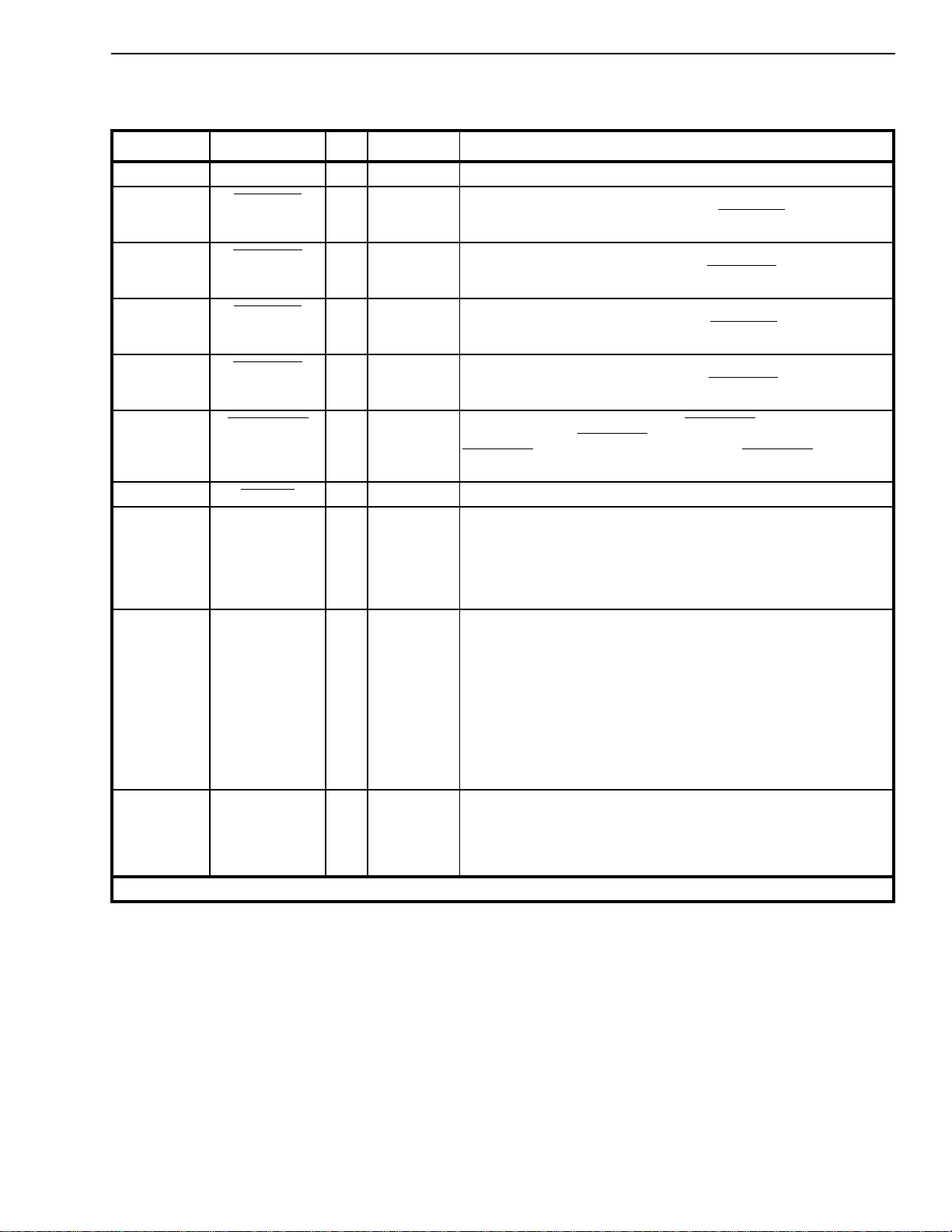
MT90500
Table 4 - External Memory Interface Pins
Pin # Pin Name I/O Type Description
98 MEMCLK O 3.3V, 4mA Memory Clock. Internally connected to MCLK.
147 MEM_CS0L O 3.3V, 4mA Active LOW memory chip select signal. This chip select is used in all memory
modes. When there are two chips per bank, MEM_CS0L is associated with
MEM_DAT[15:0] of Bank 0.
176 MEM_CS0H O 3.3V, 4mA Active LOW memory chip select signal. This chip select is used when there
are two 16-bit memory chips per bank. MEM_CS0H is associated with
MEM_DAT[31:16] of Bank 0.
148 MEM_CS1L O 3.3V, 4mA Active LOW memory chip select signal. This chip select is used when there
are two banks and two chips per bank. MEM_CS1L is associated with
MEM_DAT[15:0] of Bank 1.
177 MEM_CS1H O 3.3V, 4mA Active LOW memory chip select signal. This chip select is used when there
are two banks and two chips per bank. MEM_CS1H is associated with
MEM_DAT[31:16] of Bank 1.
178, 179, 149,
150
180 MEM_OE O 3.3V, 4mA Active LOW output enable.
123, 122, 121,
118, 117, 116,
115, 103, 102,
99, 146, 144,
130, 128, 127,
126, 125, 124
166, 167, 168,
170, 171, 173,
174, 175, 153,
154, 155, 156,
158, 159, 162,
164, 133, 134,
135, 136, 137,
138, 142, 143,
105, 106, 107,
108, 109, 112,
113, 114
165, 152, 131,
104
Note: MT90500 3.3 V CMOS inputs are pulled up to the 3.3 Volt rail. See Table 76 on page 112.
MEM_WR[3:0] O 3.3V, 4mA Active LOW byte-write enables. MEM_WR[3] is associated with
MEM_DAT[31:24]; MEM_WR[2] is associated with MEM_DAT[23:16];
MEM_WR[1] is associated with MEM_DAT[15:8]; MEM_WR[0] is associated
with MEM_DAT[7:0].
MEM_ADD[17:0] O 3.3V, 4mA Memory address lines.
MEM_DAT[31:0] I/O 3.3V CMOS
PU / 3.3V 4mA
MEM_PAR[3:0] I/O 3.3V CMOS
PU / 3.3V 4mA
Memory data lines. MEM_DAT[31:24] represent the upper byte;
MEM_DAT[23:16] represent the upper-middle byte; MEM_DAT[15:8]
represent the lower-middle byte; MEM_DAT[7:0] represent the lower byte.
Memory parity lines. MEM_PAR[3:0] are the optional “parity” bits that allow
TDM Read Underrun detection. MEM_PAR[3] is related to MEM_DAT[31:24],
MEM_PAR[2] is related to MEM_DAT[23:16], MEM_PAR[1] is related to
MEM_DAT[15:8], and MEM_PAR[0] is related to MEM_DAT[7:0]. When
unused, these pins must be pulled up via external resistors.
21
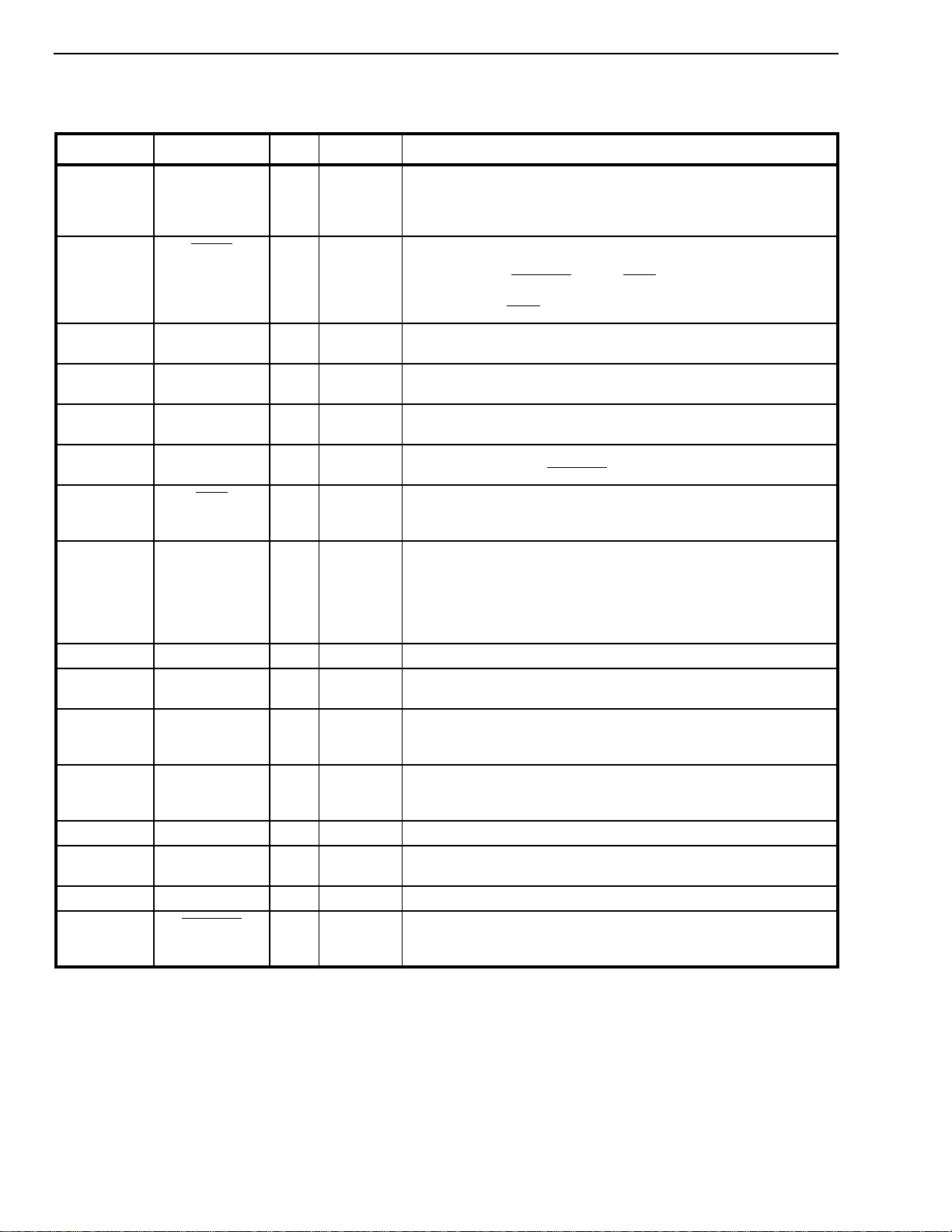
MT90500
Table 5 - Master Clock, Test, and Power Pins
Pin # Pin Name I/O Type Description
87 MCLK I TTL PU Master Clock. This signal drives the internal logic (including the RX_SAR and
the TX_SAR) and the external memory (through MEMCLK). 60 MHz for most
applications. MCLK should be more than 5 times CLKx1, and should be more
than 3 times FNXI.
78 RESET I 5V TTL
Schmitt PU
97 TMS I 3.3V CMOSPUJTAG Test Mode Select signal.
93 TCK I 3.3V CMOSPUJTAG Test Clock.
95 TDI I 3.3V CMOSPUJTAG Test Data In.
96 TDO O 3.3V, 4mASRJTAG Test Data Out.
94 TRST I 3.3V CMOSPDJTAG Test Reset input (active LOW). Should be asserted LOW on power-up
1, 7, 16, 29, 43,
61, 86, 91, 110,
119, 129, 139,
151, 163, 172,
182, 197, 213,
229
100, 141, 161 CORE_VSS GND Ground for core logic.
20, 40, 80, 201,
221
92, 111, 120,
132, 145, 157,
169, 181
2, 13, 24, 42,
60, 88, 183,
207, 225, 240
101, 140, 160 CORE_VDD_3V PWR Power for core logic (3.3 V).
21, 41, 81, 200,
220
89 IC I IC TEST, must be grounded.
90 TRISTATE I 3.3V CMOS
IO_VSS GND Ground for I/O logic.
RING_VSS GND Ground for core logic.
IO_VDD_3V PWR Power for I/O logic (3.3 V).
IO_VDD_5V PWR Power for I/O logic (5 V).
RING_VDD_3V PWR Power for core logic (3.3 V).
PU
3.3V ONLY
Chip reset signal (active LOW). Note that the MT90500 is synchronously reset,
and that MCLK should be applied during reset. To asynchronously tristate
outputs, assert the TRISTATE pin. The TRST pin (JTAG reset) should also be
asserted LOW during chip reset. Reset should last at least 2 µs when MCLK is
60 MHz. Also see SRES bit in register 0000h.
Note: TDO is tristated by TRISTATE pin.
and during reset. Must be HIGH for JTAG boundary-scan operation. Note:
This pin has an internal pull-down.
Output Tristate Control. Asynchronously tristates all output pins when LOW.
Can be asserted LOW on power-up and during reset. Pull up to 3.3V for
normal operation. NOT 5V TOLERANT.
22

Table 6 - TDM Port Pins
Pin # Pin Name I/O Type Description
MT90500
25, 23, 22, 19,
18, 17, 15, 14,
12, 11, 10, 9,
8, 6, 5, 4
230 CLKx2PI I Diff + Differential clock signal input (+) running at twice the serial TDM data
227 CLKx2NI I Diff - Differential clock signal input (-) running at twice the serial TDM data
233 CLKx1 I/O TTL PU /
232 FSYNC I/O TTL PU /
30 IC I TTL PU Internal connection (must be HIGH).
32 CORSIGA /
235 CORSIGB / MC /
33 CORSIGC /
34 CORSIGD /
35 CORSIGE /
83 EX_8KA I TTL PU An 8 kHz clock input that can be used as reference in the generation of the
234 SEC8K I/O TTL PU /
226 REF8KCLK O 5V, 12mA SR An 8 kHz clock generated internally. This signal is generated from one of
224 PLLCLK I TTL PU 16.384 / 32.768 MHz TDM clock reference from external PLL.
31 FREERUN O 5V, 12mA SR Active HIGH external PLL freerun indication.
236 LOCx2 O 5V, 4mA SR Local TDM Bus Clockx2.
3 LOCx1 O 5V, 4mA SR Local TDM Bus Clockx1.
28 LSYNC O 5V, 4mA SR Local TDM Bus Frame Sync.
26 LOCSTo O 5V, 4mA SR Local TDM Bus Serial Data Out Stream.
27 LOCSTi I TTL PU Local TDM Bus Serial Data In Stream.
231 CLKx2/
228 CLKx2NO O 5V, 12mA CLKx2 Negative Output. Differential negative output clock. (Inverse of
ST[15:0] I/O TTL PU /
5V, 12mA SR
5V, 12mA SR
5V, 12mA SR
I/O TTL PU /
CLKFAIL
FNXI
MCTX /
SRTSENA
MCRX /
SRTSDATA
MCCLK
CLKx2PO
5V, 12mA SR
I/O TTL PU /
5V, 12mA SR
I/O TTL PU /
5V, 4mA SR
I/O TTL PU /
5V, 4mA SR
I/O TTL PU /
5V, 4mA SR
5V, 12mA
I/O TTL PU /
5V, 12mA
TDM data streams. Used to pass PCM (voice) bytes or other data types. In
order to enable any of these pins as outputs, the GENOE bit in the TDM
Interface Control Register (6000h) must be set, as well as the appropriate
channel bits in the Output Enable Registers.
stream frequency. This pin is used only in differential clock mode (H-MVIP)
and should be tied HIGH when not in use. For normal (non-differential)
clock mode input, use CLKx2/CLX2PO pin.
stream frequency. This pin is used only in differential clock mode (H-MVIP)
and should be grounded when not in use.
Clockx1. This signal represents the CLKx2 signal divided by 2.
Frame sync. Bidirectional 8 kHz reference to/from main TDM Bus.
CORSIGA I/O when not used by the TDM bus. Clock fail on SCSA bus.
CORSIGB I/O when not used by the TDM bus. Message Channel (I/O) on
the SCSA bus. SRTS FNX Network Clock Input - this input line is required
when SRTS clock recovery mode is used. Note: When used for clock
recovery, this clock must be < MCLK / 3.
CORSIGC I/O when not used by the TDM bus. Message Channel Transmit
(input) toward SCSA bus from HDLC controller. This signal represents
SRTS ENA output when SRTS clock recovery mode is selected.
CORSIGD I/O when not used by the TDM bus. Message Channel Receive
(output) from SCSA bus toward HDLC controller. This signal represents
SRTS DATA output serial line when SRTS clock recovery mode is
selected.
CORSIGE I/O when not used by the TDM bus. Message Channel HDLC
controller clock (output) from the SCSA bus.
REF8KCLK or SEC8K lines.
Secondary alternate 8 kHz clock. Compatible with MVIP and H-MVIP
modes.
several internal sources which are programmed by the user. This output
can provide a reference clock to an external PLL to generate the 16.384 /
32.768 MHz required for the operation of the IC in master mode.
CLKx2 Input/Output / CLKx2 Positive Output. Normal (non-differential)
CLKx2 input in TDM Clock Slave mode. CLKx2 output (differential and nondifferential) in TDM Clock Master mode.
CLKx2PO). Used in TDM Clock Master, differential clock mode (H-MVIP);
active whenever MT90500 is TDM Clock Master. (Leave unconnected if
non-differential clock desired.)
23

MT90500
Table 7 - Reset State of I/O and Output Pins
Pin Name I/O Reset State Additional Control Information
PTXDATA[7:0] O Active during and after reset. N / A
PTXPAR O Active during and after reset. N / A
PTXCLK I/O High-impedance The PTXCLK_SEL bits in the Main Control Register (0000h) are LOW
after reset; PTXCLK is tristated and an input.
PTXEN O Active during and after reset. N / A
PTXSOC O Active during and after reset. N / A
STXCLAV O Active during and after reset. N / A
MEMCLK O Continues to drive at MCLK
rate during reset.
MEM_CS[1:0][H:L] O Active during and after reset. N / A
MEM_WR[3:0] O Active during and after reset. N / A
MEM_OE O Active HIGH during reset. RESET LOW forces this pin HIGH. After reset, this pin goes LOW.
MEM_ADD[17:0] O Active during and after reset. N / A
MEM_DAT[31:0] I/O High-impedance N / A
MEM_PAR[3:0] I/O High-impedance N / A
RDY/DTACK O Active during and after reset.
Tristated when CS is HIGH.
INT O High-impedance The interrupt enable bits in the Main Control Register at 0000h are reset to
D[15:0] I/O High-impedance N / A
TDO O Determined by TRST and / or
TAP controller state
ST[15:0] I/O High-impedance The GENOE bit in the TDM Interface Control Register (6000h) is LOW
CLKx1 I/O Input The CLKMASTER bit in the TDM Bus Type Register (6010h) resets to ‘0’;
FSYNC I/O Input The CLKMASTER bit in the TDM Bus Type Register (6010h) resets to ‘0’;
CORSIGA/
CLKFAIL
CORSIGB / MC /
FNXI
CORSIGC / MCTX /
SRTSENA
CORSIGD / MCRX /
SRTSDATA
CORSIGE
/ MCCLK
SEC8K I/O Input The SEC8KEN bit in the Master Clock Generation Control Register
REF8KCLK O Active during and after reset. Due to the reset values of the Master Clock Generation Control Register
FREERUN O Active HIGH during and after
LOCx2 O Active during and after reset. N / A
LOCx1 O Active during and after reset. N / A
I/O Input The TDM I/O Register at 6004h resets to all zeroes; all CORSIGxCNF are
I/O Input See CORSIGA.
I/O Input See CORSIGA.
I/O Input See CORSIGA.
I/O Input See CORSIGA.
reset.
N / A
In Motorola mode, pin drives HIGH during reset. In Intel mode, drives LOW
during reset.
zero; interrupts are masked after reset.
N / A
after reset; these TDM data pins are tristated and in loopback mode.
the MT90500 is TDM Slave, and CLKx1 is input from the TDM bus.
the MT90500 is TDM Slave and FSYNC is input from the TDM bus.
set to “00” and all CORSIGx pins are configured as inputs.
(6090h) resets to ‘0’; SEC8K is an input.
(6090h) and the Master Clock / CLKx2 Division Factor (6092h),
REF8KCLK is initially equal to MCLK / 8194.
The FREERUN bits in the Master Clock Generation Control Register at
6090h are “00” after reset; the FREERUN pin is reset to active HIGH.
24
MT90500
Table 7 - Reset State of I/O and Output Pins
Pin Name I/O Reset State Additional Control Information
LSYNC O Active during and after reset. N / A
LOCSTo O Active during and after reset. N / A
CLKx2/CLKx2PO I/O Input The CLKMASTER bit in the TDM Bus Type Register (6010h) resets to ‘0’;
the MT90500 is TDM Slave and CLKx2 is input from the TDM bus.
CLKx2NO O High-impedance The CLKMASTER bit in the TDM Bus Type Register (6010h) resets to ‘0’;
the MT90500 is TDM Slave and therefore no clock signals are driven from
the MT90500.
Note: All pins are placed in high-impedance by asserting the TRISTATE pin.
Table 8 - Pinout Summary
Type Input Output I/O Power Ground
Primary UTOPIA 13 11 1
Secondary UTOPIA 11 1
External Memory Interface 28 36
Microprocessor Interface 21 2 16
Miscellaneous 8 1
TDM Interface 6 7 25
Power 26
Ground 27
Total
187 + 26 + 27 = 240
59 50 78 26 27
25

MT90500
MEM_OE
MEM_WR2
MEM_WR3
MEM_CS1H
MEM_CS0H
MEM_DAT24
MEM_DAT25
MEM_DAT26
IO_VSS
MEM_DAT27
MEM_DAT28
IO_VDD_3V
MEM_DAT29
MEM_DAT30
MEM_DAT31
MEM_PAR3
MEM_DAT16
IO_VSS
MEM_DAT17
CORE_VDD_3V
MEM_DAT18
IO_VDD_3V
CORE_VSS
MEM_DAT20
MEM_DAT19
MEM_DAT21
MEM_DAT22
MEM_DAT23
MEM_PAR2
IO_VSS
IO_VDD_3V
IO_VSS
IO_VDD_5V
AEM
A15
A14
A13
A12
A11
A10
A9
A8
A7
A6
A5
A4
IO_VSS
A3
RING_VDD_3V
IO_VDD_5V
RING_VDD_3V
IO_VDD_5V
CLKx2/CLKx2PO
RDY/DTACK
IO_VDD_5V
A2
RING_VSS
A1
CS
D0
D1
D2
D3
D4
D5
D6
D7
IO_VSS
D8
D9
D10
D11
D12
D13
RING_VSS
D14
D15
PLLCLK
REF8KCLK
CLKx2NI
CLKx2NO
IO_VSS
CLKx2PI
FSYNC
CLKx1
SEC8K
CORSIGB
LOCx2
WR/R\W
RD/DS
182
184
186
188
190
192
194
196
198
200
202
204
206
208
210
212
214
216
218
220
222
224
226
228
230
232
234
236
238
240
240 PIN PQFP
22 24 26 28 30
2018161412108642
152154156158160162164166168170172174176178180
26
ST0
ST1
ST2
ST3
ST4
ST5
ST6
ST7
ST8
LOCx1
IO_VSS
IO_VDD_5V
IO_VSS
ST9
IO_VDD_5V
Figure 2. Pin Connections
ST10
ST11
IO_VSS
ST12
ST13
RING_VSS
RING_VDD_3V
ST14
ST15
LOCSTo
IO_VDD_5V
LSYNC
LOCSTi
IO_VSS
IC
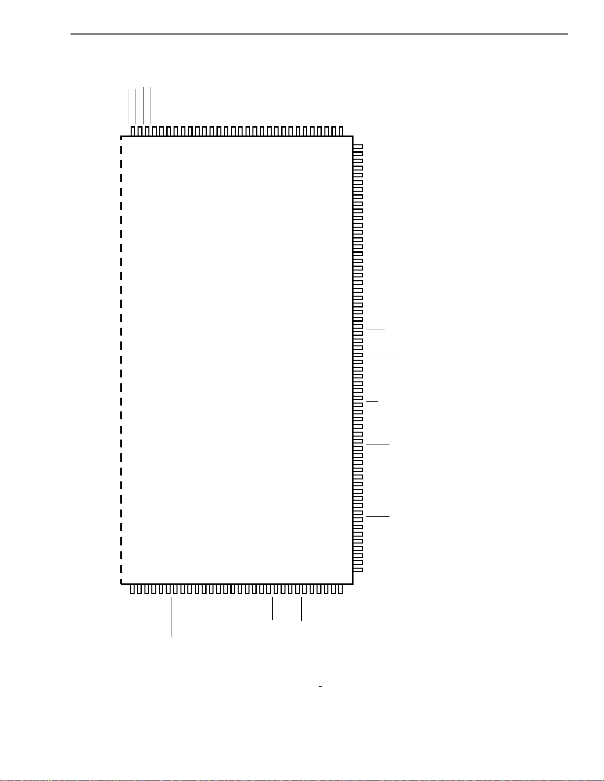
MEM_WR0
MEM_WR1
MEM_CS1L
MEM_CS0L
MEM_ADD7
IO_VDD_3V
MEM_ADD6
MEM_DAT8
MEM_DAT9
CORE_VDD_3V
IO_VSS
MEM_DAT10
MEM_DAT11
CORE_VSS
MEM_DAT12
MEM_DAT13
MEM_DAT14
MEM_DAT15
IO_VDD_3V
MEM_PAR1
MEM_ADD5
IO_VSS
MEM_ADD4
MEM_ADD3
MEM_ADD2
MEM_ADD1
MEM_ADD0
MEM_ADD17
MEM_ADD16
MT90500
MEM_ADD15
240 PIN PQFP
122124126128130132134136138140142144146148150
52 54 56 58 6050484644424038363432
120
118
116
114
112
110
108
106
104
102
100
98
96
94
92
90
88
86
84
82
80
78
76
74
72
70
68
66
64
62
IO_VDD_3V
IO_VSS
MEM_ADD14
MEM_ADD13
MEM_ADD12
MEM_ADD11
MEM_DAT0
MEM_DAT1
MEM_DAT2
IO_VDD_3V
IO_VSS
MEM_DAT3
MEM_DAT4
MEM_DAT5
MEM_DAT6
MEM_DAT7
MEMPAR0
MEM_ADD10
MEM_ADD9
CORE_VDD_3V
CORE_VSS
MEM_ADD8
MEMCLK
TMS
TDO
TDI
TRST
TCK
IO_VDD_3V
IO_VSS
TRISTATE
IC
IO_VDD_5V
MCLK
IO_VSS
STXCLK
INT
EX_8KA
PTXCLK
RING_VDD_3V
RING_VSS
PRXCLK
RESET
STXDATA0
STXDATA1
STXDATA2
STXDATA3
STXDATA4
STXDATA5
STXDATA6
STXDATA7
STXSOC
STXEN
STXCLAV
PRXDATA0
PRXDATA1
PRXDATA2
PRXDATA3
PRXDATA4
IO_VSS
CORSIGA
CORSIGC
CORSIGD
FREERUN
IC
CORSIGE
PTXDATA0
MOTOROLA
INTEL/
RING_VSS
PTXDATA1
IO_VDD_5V
RING_VDD_3V
IO_VSS
PTXDATA2
PTXDATA3
PTXDATA4
PTXDATA5
PTXDATA6
PTXDATA7
PTXEN
PTXPAR
PTXSOC
PRXEN
PRXSOC
PTXCLAV
PRXCLAV
PRXDATA7
PRXDATA6
PRXDATA5
IO_VDD_5V
27

MT90500
4. Functional Description
As shown in Figure 1, “MT90500 Block Diagram,” on page 12, the MT90500 device consists of the following
major components: TDM Module, External Memory Controller, TX_SAR, RX_SAR, UTOPIA Module, Clock
Recovery, Microprocessor Interface, and Test Interface. This section descr ibes each module in detail.
4.1 TDM Module
This circuit module is the interface to the Time Division Multiplexed (TDM) buses, which carry N x 64kbps data.
The TDM module interfaces are:
• 16 bidirectional TDM data streams on pins ST[15:0]; these pins can be configured through soft-
ware registers to support various bus formats (ST-BUS, MVIP, H-MVIP, SCSA, or IDL) and data
rates of 2.048 Mbps, 4.096 Mbps, or 8.192 Mbps; (F or the selection of the b us type , see TDM Bus
Type Register at address 6010h in Section 5.)
• the TDM bus clocks (CLKx2, CLKx1) and frame synchronization signal (FSYNC);
• the TDM bus ancillary signals such as SEC8K (MVIP) and CLKFAIL (SCSA);
• a local TDM bus (LOCx2, LOCx1, LSYNC, LOCSTi, and LOCSTo); the format of the bus, which
runs at 2.048 Mbps (LOCx2 = 4.096 Mbps), is user-programmable via software (see Local Bus
Type Register at address 6020h).
The TDM module moves TDM data from the TDM serial inputs to the external memory (where it is read by the
TX_SAR) in the transmit direction, and from the external memory (where it was written by the RX_SAR) to the
TDM outputs in the receive direction. This is done with the aid of an internal TDM frame buff er, which is used to
buffer 4 frames of each TDM channel in both directions; i.e. four frames in the receive direction (ATM to TDM),
and four frames in the transmit direction (TDM to ATM). The TDM module can be divided into four main
processes:
• TDM Clock Logic, which controls all the operations related to clock generation and clock signal
monitoring on the TDM bus;
• TDM Interface Operation, which controls the input and output of the serial TDM data;
• TDM Data to External Memory Process, which transfers TDM input data into Transmit Circular
Buffers in the external memory;
• External Memory to TDM Data Output Process, which transfers TDM output data from Receive
Circular Buffers in the external memory to the TDM output bus.
Each of these processes are described in detail below.
4.1.1 TDM Clock Logic
The TDM Clock Logic controls all of the operations related to clock generation and clock signal monitoring on
the TDM bus. The block diagram of the TDM Clock Logic is shown in Figure 3. This module consists of several
blocks, including: selection logic for an 8 kHz reference for the external PLL (REF8KCLK), the main TDM bus
clock generation logic, the local TDM bus clock generation logic, the clock drivers & clock selection for the
SEC8K signal, and the clock failure detection logic.
4.1.1.1 TDM Timing Modes
The MT90500 supports 4 major TDM timing modes. There are also a number of TDM timing features which are
independent of the TDM timing mode being used:
• The SEC8K pin (MVIP compatibility) can be programmed as either output or input. The SEC8KEN
bit in the MCGCR Register (6090h) enables the SEC8K pin driver. If the SEC8K pin is enabled as
an output, the SEC8KSEL bit in the same register selects the source for this signal (the EX_8KA
input, or the internal 8 kHz FS_INT signal which is derived from CLK16).
28
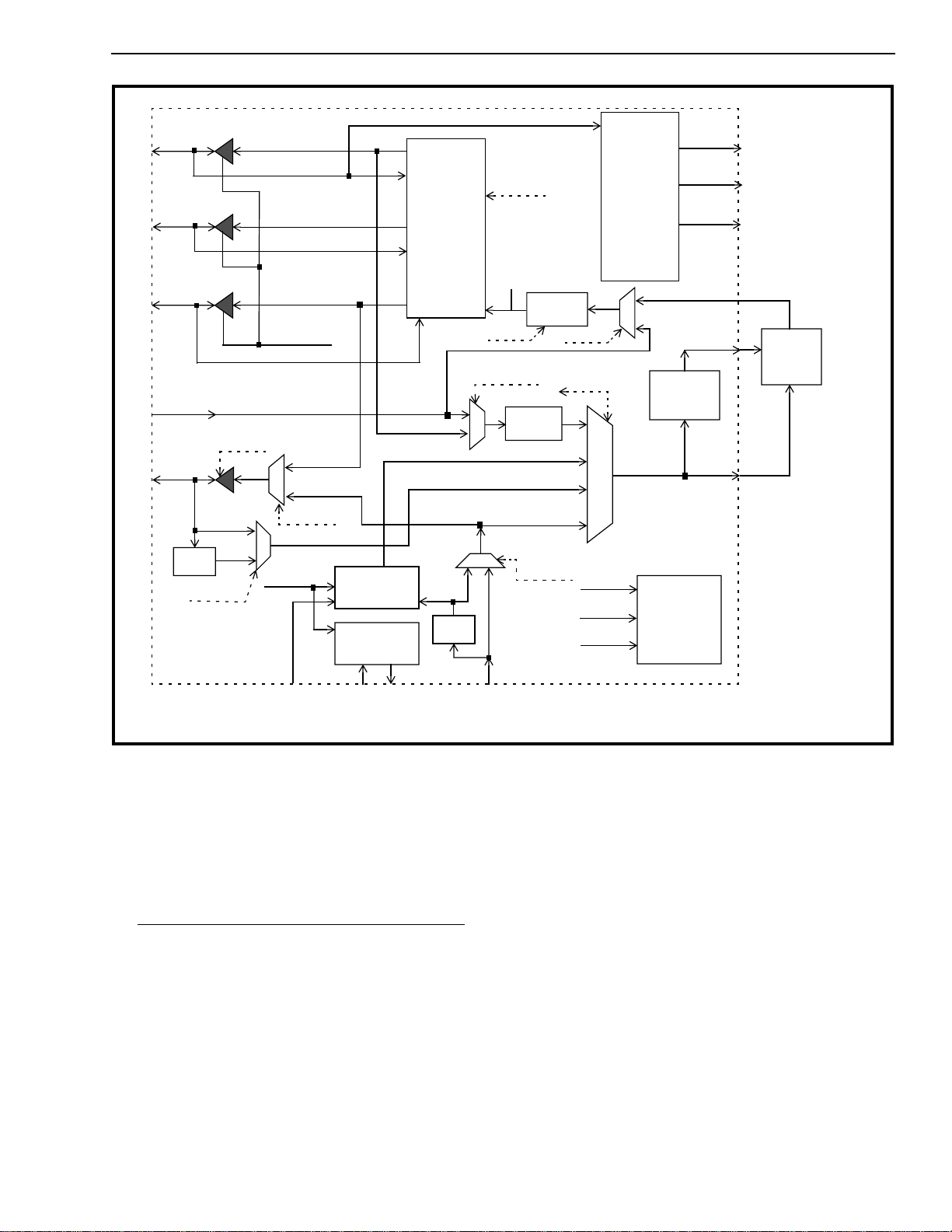
MT90500
CLKx2
CLKx1
Main TDM Bus
FSYNC
MCLK
SEC8K
Square
SEC8K_SQ
MT90500
Master/Slave
SEC8KEN
1
0
SEC8KSEL
0
1
ATM Cells
Internal CPU Bus
External CPU Bus
FS_INT
FSYNC
FS_INT
EX_8KA_INT
SRTS Clock
FNXI
Adaptive
Clock
Recovery
Recovery
Main TDM
Bus Timing
Generation
SRTS
and
Clock
Logic
Square
LOCx2
PHLEN
CLK16
(16.384 MHz)
Divide by
1,2,4,or 8
DIV1...8
DIVCLK_SRC
0
Divide by 2
to 16384
1
RXVCLK
SEC8K_INT
EX_8KA_INT
10
EX_8KA
All control bits shown are in Master Clock Generation Control Register (6090h).
BEPLL
REFSEL<1:0>
EX_8KA_SQ
Local TDM
Bus
Clock
Generation
Logic
1
0
0
1
2
3
CLKx2
CLKx1
FSYNC
LOCx1
LSYNC
PLLCLK
FREERUN
REF8KCLK
Detection
Logic
REF8KCLK
Clock Absent
Detection
Logic
Local TDM Bus
MT9041 or
other PLL
External
PLL
(Optional)
Figure 3 - TDM Clock Selection and Generation Logic
• The CLKx2 signal can be selected as single-ended or differential. (Differential CLKx2 allows com-
patibility with the H-MVIP bus.) In TDM Timing Slav e, the CLKx2 signal can be input on the CLKx2
pin, or the differential CLKx2PI and CLKx2NI pins. This selection is made with CLKTYPE in the
TDM Bus Type Register at address 6010h. In TDM Timing Master, the CLKx2 signal is output on
the CLKx2/CLKx2PO pin, and an inverted clock is available on the CLKx2NO pin.
The MT90500 supports the following TDM timing modes:
• TDM Timing Bus Slave - CLKx2 Reference (CLKMASTER = ‘0’ in TDM Bus Type Register at 6010h)
In this mode, the MT90500 is configured as a TDM Timing Slave and all internal TDM timing is synchronized to
the TDM clock inputs: CLKx2, CLKx1, and FSYNC. The following sub-modes are also selectable:
• The CLKx1 can be an input at the CLKx1 pin, or it can be derived internally from CLKx2. This is
controlled by TCLKSYN (address 6010h). If the CLKx1 pin is not used as an input in TDM Slave
mode, it remains high-impedance.
• TDM Timing Slave operation takes its 8 kHz framing from the FSYNC input pin, which would usu-
ally be driven by the TDM bus. To support other implementations, the REF8KCLK output remains
active in TDM Slave mode. An 8 kHz reference output can be made available at REF8KCLK,
selectable from the EX_8KA input, the SEC8K pin, or one of the internal dividers. In addition, the
FREERUN output can be used to monitor the presence of REF8KCLK.
29

MT90500
• TDM Timing Bus Master - Freerun (CLKMASTER = ‘1’ in TDM Bus Type Register at 6010h)
In this mode, the MT90500 is configured as the TDM Timing Master and the MT90500 drives the three TDM
bus clocks: CLKx2, CLKx1, and FSYNC . The MT90500 cloc k gener ator b lock uses either the MCLK input or the
PLLCLK input to generate all of the required clocks. Typically in this mode MCLK or PLLCLK is connected to an
oscillator, and no other synchronization source is used. Several selections must be made:
• The selection of MCLK or PLLCLK is determined by the BEPLL bits in the Master Clock Genera-
tion Control Register at 6090h.
• The selected clock is divided by 1, 2, 4, or 8 to obtain a 16.384 MHz clock, called CLK16. This divi-
sion is controlled by the DIV1...8 bits at 6090h.
• TDM Timing Bus Master - 8 kHz Reference (CLKMASTER = ‘1’ in TDM Bus Type Register at 6010h)
In this mode, the MT90500 is configured as the TDM Timing Master and the MT90500 drives the three TDM
bus clocks, synchronized to one of several possible 8 kHz references. Typically, in this mode, the PLLCLK input
is driven by an external PLL (such as the Mitel MT9041), which is controlled by the REF8KCLK and FREERUN
outputs. The following options are also selectable:
• One of four 8 kHz reference sources must be selected, using the REFSEL bits at 6090h. (See
Figure 3 and Section 4.1.1.2 for further details.)
• If the external PLL is controlled by the FREERUN output pin, the pin’s operation must be specified
by the FREERUN bits at 6090h. The CPU can force the FREERUN pin to either state, or allow the
FREERUN pin to follow the REF8KCLK failure-detection bit (REFFAIL at 6082h).
• Bus Master-Alternate (CLKMASTER = ‘0’, CLKALT = ‘1’ in TDM Bus Type Register at 6010h)
In this mode, the MT90500 is configured as a TDM Timing Slave, but stands ready to become the Timing
Master, should the timing on the TDM bus fail. The switch is normally automatic (based on the CLKFAIL input),
but can also performed by the CPU (for instance: by programming the chip into TDM Timing Master following a
Clock Absent interrupt). The following options are also selectable:
• To make the switch from Alternate to Master automatic, several settings are required: CLKALT at
6010h is set HIGH, and the CORSIGA pin is configured as the CLKFAIL input (CORSIGACNF =
“11” at 6004h).
• The Master-Alternate operates normally as a TDM Timing Slave, and has the same options as the
TDM Timing Slave listed above.
• The Master-Alternate can be set up to switch to Master-Freerun operation, should the TDM bus
clocks fail. The same options as listed above for Master-Freerun apply to this mode.
• The Master-Alternate can be set up to switch to Master-8 kHz Reference operation, should the
TDM bus clocks fail. The same options as listed above for Master-8 kHz Reference apply to this
mode. Additionally, REF8KCLK can be obtained from the TDM bus by dividing CLKx2. This allows
the external PLL to be phase-locked to the TDM bus clocks. Note that in this case the FREERUN
output should be set up to automatically place the external PLL in freerun should the TDM bus
clocks fail.
• The internal 8 kHz (FS_INT) of the Master-Alternate can be phase-locked to the TDM bus FSYNC
by setting PHLEN = ‘1’ at 6090h. (This is only valid when the FSYNC type at 6010h is set to “00”.)
This will align the internal “stand-by” FSYNC, CLKx2, and CLKx1 to the TDM bus to within a clock
cycle of the internal 16.384 MHz clock, allowing for minimal phase-shift should the Master-Alternate MT90500 take over the TDM bus clocks.
4.1.1.2 REF8KCLK Selection Logic
The REF8KCLK output pin of the MT90500 is intended to provide a clock ref erence to an optional external PLL.
This signal would usually be an 8 kHz frame pulse, but other signals are possible. The external PLL (e.g. Mitel
MT9041) can be used to multiply the REF8KCLK output to 16.384 MHz (or 32.768 MHz) and attenuate jitter.
The 16.384 MHz can then be applied to the PLLCLK input pin to allow the MT90500 to generate the TDM
30

MT90500
clocks: CLKx2, CLKx1 and FSYNC. The source for the REF8KCLK signal is selected via the REFSEL bits at
address 6090h. The four possible sources for REF8KCLK are:
• a clock input signal pin operating at 8 kHz (EX_8KA)
• a secondary 8 kHz reference from the TDM bus (SEC8K, compatible with MVIP/H-MVIP)
• a freerun mode clock, which is a divided-down version of CLKx2 or MCLK; selected by
DIVCLK_SRC in register 6090h, and divided as specified in register 6092h
• RXVCLK, a more precisely divided-down version of MCLK from the Adaptive Clock Recovery
block. The division is controlled by registers 60A8h and 60AAh.
The REF8KCLK signal is made available on the output pin whether the MT90500 is programmed to be TDM
Timing Master or Slave.
Also included in the MT90500 is circuitry to convert the SEC8K signal and the EX_8KA signal into square
waves. If the SEC8K_SQ control bit in register 6090h is set HIGH, inter nal logic will convert the SEC8K input
signal into a square wave before passing it to the REF8KCLK selection multiplexer. The EX_8KA_SQ bit
controls the squaring function for the EX_8KA signal. See the register 6090h. Mitel PLLs will typically work with
either a pulse 8 kHz, or a square 8 kHz, but other PLL implementations may require a square 8 kHz reference
input.
4.1.1.3 Main TDM Bus Timing and Clock Generation Logic
When the MT90500 is in the TDM Timing Master mode, this logic generates the main TDM bus clocks (CLKx2,
CLKx1, and FSYNC). This block receives CLK16 (a 16.384 MHz clock which is a divided-down version of either
PLLCLK or MCLK, as set in register 6090h) and outputs the generated TDM bus clocks. By programming the
appropriate software registers (i.e. TDMTYP at address 6010h), the generated signals can be 16.384MHz/
8.192MHz/4.096MHz, 8.192MHz/4.096MHz/2.048MHz, and 8 kHz respectively. Additionally, the TDM Bus
Clock Generation Logic generates a source signal to the SEC8K output line when the SEC8KEN register bit is
enabled.
When in TDM Timing Slave mode, or in Master-Alternate mode, this logic generates an internal stand-by 8 kHz
signal (FS_INT), from the clock selected by BEPLL in register 6090h. This can be driven out on SEC8K if
enabled by SEC8KEN.
4.1.1.4 TDM Clock Drivers
If the MT90500 is the TDM Timing Master, this block enables the clock drivers for CLKx2, CLKx1, and FSYNC.
If the MT90500 is in Slave mode, the drivers are disabled and CLKx2, CLKx1, and FSYNC are inputs to the
MT90500. In Slave mode, the CLKx1 source can be separately selected between the CLKx1 input or internally
provided CLKx2/2. These options are controlled by the TDM Bus Type Register at 6010h.
4.1.1.5 Clock Failure Detection
There are three status bits related to the detection of clock failure: REFFAIL (6082h), and CABS and CFAIL
(6002h). These bits will cause an interrupt if their respective enable bits are set (REFFAILIE at 6080h, and
CABSIE and CFAILIE at 6000h) and the TDM_INTE bit is set at 0000h.
The REFFAIL bit monitors the absence of the REF8KCLK signal. When this signal is absent, the clock detect
logic can activate the FREERUN output signal which is used to place the external PLL in freer un mode. Once
the REF8KCLK signal goes back to normal (due to the CPU changing the timing source), the CPU can disable
the FREERUN output signal by clearing the REFFAIL bit in the Clock Module General Status Register at
6082h. With proper selection of the external PLL, this clock failure detection circuit can help to guarantee that
the TDM clocks do not glitch when the REF8KCLK reference to the exter nal PLL changes.
The CABS bit indicates that one or more of the TDM bus clock signals (CLKx2, CLKx1, or FSYNC) are absent.
This block uses MCLK to check for activity on the above signals. In the case of clock absence, the Clock
Absent (CABS) bit in the TDM Interface Status (TIS) Register at address 6002h is activated.
The CFAIL bit monitors the CLKFAIL pin (a SCSA bus signal) and requires that the CORSIGA pin be
configured as the CLKFAIL input. If the CLKFAIL input goes HIGH when the MT90500 is operating in MasterAlternate mode (CLK_ALT at 6010h), the MT90500 will take over the TDM bus and become the Master TDM
clock source (see the Bus Master-Alternate description in Section 4.1.1).
31

MT90500
4.1.2 TDM Interface Operation
4.1.2.1 Main TDM Bus Operation
The main TDM bus (pins ST[15:0]) supports SCSA, MVIP, H-MVIP, ST-BUS, and IDL protocols. These buses
have different frame sync pulse orientations and different data sampling specifications, as well as different pin
requirements. However, all of these buses are composed of 16 data pins, as well as CLKx2, CLKx1, and
FSYNC lines.
The TDM bus type is controlled by the TDM Bus Type Register at 6010h. In all bus types, outputs change on
the rising edge of CLKx1. Inputs can be sampled at the 2/4, 3/4 or 4/4 point of the CLKx1 signal. MVIP/SCSA/
ST-BUS all use a negative FSYNC that is asserted for one CLKx2 cycle, straddling the frame boundar y. The
IDL bus uses a positive FSYNC which is asserted for one cycle of CLKx1, preceding the frame boundary. (See
Figure 39, “Nominal TDM Bus Timing,” on page 114.)
4.1.2.2 TDM Loopback
The General Output Enable bit (GENOE in the TDM Interface Control Register at 6000h) is used to enab le data
to be driven out on the TDM output streams. When this bit it not set (i.e. it is LOW), the inter nal TDM transmit
buses are connected to the internal TDM receive buses (while the internal TDM buses are disconnected from
the external TDM buses) giving a TDM loopback from ATM receive back to ATM transmit. In this mode, the
internally-generated TDM clocks and synchronization signals are used. This allows the user to test the
MT90500 in stand-alone mode by passing receive ATM cells through the SAR, through the internal loopback at
the TDM interface, and back through the SAR and out as transmit ATM cells.
4.1.2.3 Per-channel Output Enable Feature
The ST[15:0] pins are bidirectional, and are able to switch between input and output directions on a perchannel basis. The Output Enable Registers located at addresses 7000 + 2N (N = 0, 1, ..., 127) are used for
individual time slot output enable control. Depending on the TDM bus rate, up to 128 registers (256 bytes) are
used to provide up to 2048 individual channel-output-enable bits. At 2.048 Mbps, 32 registers are used; at
4.096 Mbps, 64 registers are used; and at 8.192 Mbps, 128 registers are used.
During each channel period (TDM time slot), 16 output enable bits (one register) are read from the Output
Enable Registers. Within each frame, 32, 64, or 128 registers are read (depending on the TDM bus rate). The
GENOE bit must be set HIGH, as well as the individual channel-output-enable bit, in order for a TDM channel
to be transmitted from the MT90500 onto the TDM bus. In order to prevent data collisions on the TDM bus, the
user should clear all Output Enable Register bits for channels not used as outputs, prior to setting the GENOE
bit. The GENOE signal, when inactive, asynchronously deactivates the tristate buffers on the data pins and
routes the output paths back into the input paths, causing the TDM bus to enter the TDM Loopback mode (see
Section 4.1.2.2).
Since the ST pins are bidirectional, the input sampling is always activ e and output data can be re-sampled back
into the MT90500. This re-sampling is used when LOCSTi channels are output on a ST pin and then resampled for ATM transmission, when ST outputs are re-sampled for transfer to the LOCSTo pin, or for test and
verification purposes.
4.1.2.4 Local Bus Operation
The local bus signals are:
• LOCx2, LOCx1, LSYNC - clock output signals;
• LOCSTi, LOCSTo - Local Serial TDM data in and data out.
The MT90500 provides three output clocks for the local TDM bus: LOCx2, LOCx1 and LSYNC. These clocks
are derived from CLKx2, and controlled by the relevant bits in the Local Bus Type Register (register 6020h).
The LCLKDIV bits allow LOCx2 to be equal to CLKx2, CLKx2 / 2, or CLKx2 / 4 (note that the local bus rate is
2.048 Mbps, which is always equal to, or less than, the main TDM bus rate). Also in register 6020h are the
control bits to select the LSYNC frame-pulse type, the routing of TDM streams onto and from the local bus, and
the LOCSTi sampling point.Except for the rate, the local bus type can be configured independently of the main
TDM bus type.
32

MT90500
4.1.2.5 Local Bus Data Transfer Process
A local bus data transfer process is provided, which allows local serial TDM input (LOCSTi) data to be output
on the main TDM bus (ST[15:0]) in place of the usual data from the internal frame memory. Similarly, data from
the main TDM bus can be routed directly onto the local TDM output (LOCSTo), without affecting the TDM to
internal frame memory transfer.
The local bus pins on the MT90500 are an extension of the main TDM b us. The data on any stream of the main
TDM bus may be passed to the local bus output (LOCSTo). The source pin (one of ST[15:0]) is controlled with
the STi2LOCSTo bits at 6020h, and the time slots to be transferred are indicated by the TDM Bus to Local Bus
Transfer Register (6022h). Note that this TDM data can be from two sources: either exter nally-sourced data
being driven into the selected ST pin, or data from the ATM link being driven out by the RX_SAR, and copied to
the LOCSTo pin. When fewer than the maximum number of available time slots are transferred between the
main TDM bus and the local bus, the unused LOCSTo output time slots are filled with data fed back internally
from LOCSTi.
Similarly, the data input on LOCSTi may be passed to any stream of the TDM bus as indicated by the Local Bus
to TDM Bus Transfer Register (6024h), and the LOCSTi2STo bits at 6020h. Note that when the local bus to
TDM process is enabled, from 1 to 32 data bytes from the RX_SAR will be replaced by local bus data. The
enable bits for the main TDM bus channels are the nor mal bits in the Output Enable Registers (7000h + 2N).
Data from the LOCSTi input pin can be transferred to the ATM link through the TX_SAR, by re-sampling the
channels on which the local bus data is output as inputs to the TX_SAR.
4.1.3 TDM Data to External Memory Process
4.1.3.1 General
The segmentation of serial TDM input data into ATM cells starts by copying the TDM data into Transmit Circular
Buffers. The data is then read out of the Transmit Circular Buffers by the TX_SAR (see Section 4.3.2, “TX_SAR
Process,” on page 48). The initial step of copying the serial TDM input data into the Transmit Circular Buffers is
performed by the TDM Data to External Memory Process described in this section.
TDM Buses
Internal Memory
TDM Input
Frame Buffer
Tx Circular Buffer 1
Tx Circular Buffer 2
Tx Circular Buffer 3
Tx Circular Buffer n-1
Tx Circular Buffer n
External Memory
TXCBBASE (Register 6044h)
TXCBBASE+64
TXCBBASE+128
Each active DS0
channel occupies a
64-byte Transmit
Circular Buffer.
Figure 4 - TDM Frame Buffer to External Memory Transfer
All of the serial TDM input data available on the TDM buses is first written to an internal frame buffer which
holds 4 frames of TDM data per input channel. As shown in Figure 4, this internal frame memory (which is used
in both the receive and transmit directions simultaneously) is used as a pingpong buffer. While one page of the
memory is being loaded with input TDM data, the other page of the memory is being transferred to the Transmit
Circular Buffers in external memory. This transfer occurs every 500 µs (4 frames * 125 µs per frame).
33

MT90500
4.1.3.2 Transmit Circular Buffer Control Structures
To minimize the amount of external memory required for the TDM Data to External Memory Process, only the
TDM channels assigned to be transmitted over the ATM link are transferred to external memory. Each TDM
channel to be transmitted over the ATM link occupies a 64-byte Transmit Circular Buffer in external memory. As
shown in Figure 5, the MT90500 fetches control data from the Transmit Circular Buffer Control Structure in
external memory in order to determine which TDM channels to transfer to external memory and where to put
the data. The Transmit Circular Buffer Control Structure is a sequential control table consisting of 16-bit entries:
• Bit<15> indicates that the entry is valid (active HIGH).
• Bits<14:11> are not used, and should be set to zeroes.
• Bits<10:0> identify a channel number.
• Bits<10:4> identify a TDM channel within a stream. The channels are numbered from 0 to 127.
• Bits<3:0> identify a stream number, from 0 to 15.
Internal Memory External Memory
B “0_0000_0000”
9
4
TXCBCSL
<8:0>
<20:0>
0
Minimum of 128 entries (i.e.
Maximum of 2048
Pointer to Start of
TX Circular Buffer
Control Structure
words)
entries
+000
+002
+004
+006
3
401015
R
R
V
R R
V
R R
R R
R R
V
R R
V
R R
R R
Time Slot
Time Slot Stream
Time Slot Stream
Time Slot
Stream
Stream
6040h
12 21
<20:9>
TXCBCS
15
TXCBCSBASE
V
RR
R
R
+FFE
V
RR
R
R
TDM Channels Control Data
V = Entry Valid (bit<15>)
R = Reserved (bits<14:11> - set to all zeroes)
Time Slot = 7-bit TDM time slot select (bits<10:4>)
Stream = 4-bit TDM stream select (bits<3:0>)
Time Slot Stream
Time Slot
Stream
Figure 5 - Transmit Circular Buffer Control Structure
The first entry in the Transmit Circular Buffer Control Structure tells the hardware from which TDM channel it
will fill the first 64-byte Transmit Circular Buffer, the second entry tells the hardware from which TDM channel it
will fill the second Transmit Circular Buffer, and so on. If the entry is not valid (i.e. the V bit is not asserted), the
transfer is not executed. In order to prevent unnecessary transfer of TDM data to exter nal memory, the user
should zero-out all unused entries within the TX Circular Buffer Control Structure.
34

MT90500
4.1.3.3 Transmit Circular Buffers
The location of the Transmit Circular Buffers in external memory is determined by TXCBBASE (TX Circular
Buffer Base Address), found in register 6044h. The first Transmit Circular Buffer is located at TXCBBASE. The
second is located at TXCBBASE + 64, the third at TXCBBASE + 128, etc., as seen in Figure 4. All Transmit
Circular Buffers are 64 bytes long, so buffer addresses are not included in the control structure but are
considered to follow each other linearly, one after the other, corresponding to the order of the entries in the
control structure. Therefore, if the base address of the TX Circular Buffers was 10000h (as defined by the
TXCBBASE entry at 6044h), the first entry in the control str ucture (be it valid or not) would correspond to the
buffer at 10000h, the next to 10040h, the one after to 10080h, etc.
The last step of the TDM Data to External Memory Process transfers data from the internal frame buffer to the
Transmit Circular Buffers in external memory. The write pointer to all Transmit Circular Buffers is a single 8-bit
counter that increments every four frames as the Internal to External Memory transfer is performed. The 4 least
significant bits in this counter are used as the TDM Circular Buffer Write Pointer. All the desired TDM channels
in the internal frame buffer will be transferred into the Transmit Circular Buffers as specified by the Transmit
Circular Buffer Control Structure. Note that the Transmit Circular Buffer Control Str ucture must be initialized
before the Internal/External Memory Process is enabled (via the IEENA bit in register 6000h).
4.1.4 External Memory to TDM Data Output Process
4.1.4.1 General
The reassembly of received CBR (Constant Bit Rate) ATM cells into serial TDM output data is completed by
reading the data out of Receive Circular Buffers and placing the data on the TDM outputs . The data is written to
the Receive Circular Buffers by the RX_SAR (see Section 4.4.2, “RX_SAR Process,” on page 57). Then the
reading of serial TDM output data from the Receive Circular Buffers is perfor med by the External Memory to
TDM Data Output Process. This process will be outlined here.
The same internal frame buffer used in the TDM Data to External Memory Process is used to buffer the
received data to be transferred to the TDM output bus. As shown in Figure 6, this internal frame buffer holds 4
frames of output data for each TDM channel (to a maximum of 2,048 channels). This frame buffer is used in a
pingpong scheme where alternately half the memory is used to transfer data to the TDM buses while the other
half is being used to transfer data from the external memory. TDM data is transferred from the Receive Circular
Buffers in external memory to the internal frame buffer. As in the TDM Data to External Memory Process
described previously, the pointer to all Receive Circular Buffers is a single 8-bit counter that increments every
four frames as the External to Internal Memory transfer is performed. The least significant 4 to 8 bits of the
counter are used as the TDM Circular Buffer Read Pointer, depending on the size of the Receive Circular
Buffers.
Internal Memory
TDM Output
Frame Buffer
TDM Buses
Each active DS0
channel occupies a
programmable-size
Receive Circular
Buffer (64, 128, 256,
512, or 1024 bytes)
External Memory
Rx Circular Buffer 1
Rx Circular Buffer 2
Rx Circular Buffer 3
Rx Circular Buffer n-1
Rx Circular Buffer n
Figure 6 - External Memory to TDM Frame Buffer Transfer
35

MT90500
4.1.4.2 External Memory to Internal Memory Control Structures
To know which internal frame buffer TDM channels need to be written (generally, only the TDM channels
scheduled for transmission on the TDM bus), the MT90500 uses control data from the External to Internal
Memory Control Structure. The External to Inter nal Memory Control Structure is located in external memor y,
and is depicted in Figure 7. The control data in the External to Internal Memory Control Structure tells the
hardware where in external memory the receive data is located (Rx Circ. Buf. Address), the size of the Receive
Circular Buffer used, and to which TDM channel (TDM Channel #) this data must be written.
The External to Internal Memory Control Structure uses a 32-bit control word, as indicated below and in
Figure 7:
• Bit<15> - V - Valid bit. If HIGH, indicates that this entr y is valid, and the associated Receive Circular
Buffer is active. If an entr y is not valid, it is simply bypassed and the next entry is read.
• Bit<14> - D - Write-back Disable bit. If HIGH, the receive TDM data will be left unaltered in the Receive
Circular Buffer. If LOW, FFh will be written over each byte of the receive TDM data once it has been
transferred to the internal frame memory. (This has the effect of putting FFh - silence - on the TDM bus
if the Receive Circular Buffer underruns and the same byte is read again before new TDM output data is
written to the Receive Circular Buffer by the RX_SAR.)
• Bit<13> - U - TDM read Underrun detection enable. If this bit is HIGH, and the External Memory to
Internal Memory Process tr ies to transfer a byte which has already been transferred, an underrun event
is detected and an interrupt may be generated. See registers 6000h, 6002h, 6046h and 6048h. This bit
(and TDM Read Underrun Detection circuit) work independently of the state of the ‘D’ bit. If this bit is
written low, TDM Read Underrun detection stops for this TDM channel on the present TDM frame.
• Bits<12:11> - R - Not used.
• Bits<10:0> - TDM Channel # - identifies a destination TDM channel number and stream
• Bits<10:4> identify a TDM channel within a TDM stream. The channels are numbered from 0 to
127.
• Bits<3:0> identify a TDM stream number, from 0 to 15 (corresponding to the ST[0:15] pins).
• Rx Circ. Buff. Address and Size - indicates the Receive Circular Buffer address, and the size of the
Receive Circular Buffer (64, 128, 256, 512, or 1,024 b ytes). The leading bits in the field, when appended
by a number of least-significant zeroes, indicate the Receive Circular Buffer address. The total number
of bits representing an address should be 21 bits. For example, for a 128-byte buffer, the 14-bit address
given in the structure will be appended by 7 zeroes, resulting in a 21-bit address.
It is important to consider this control structure when deter mining the location of Receive Circular Buffers in
external memory. Examining the configuration shown in Figure 7 on the next page, it can be seen that the
number of bits available to identify the address of Receive Circular Buffers differs depending on the size of the
buffer. Due to this restriction, it is essential that each buffer be located only on a boundary corresponding to the
size of the buffer (i.e. 64-byte buffers must be located on 64-byte boundaries, 128-byte buffers must be located
on 128-byte boundaries, and so on...).
Once all of the entries have been scanned, the internal frame memory is filled and the External Memor y to
Internal Memory process terminates. If the process is still active four frames after being started, a “TDM Out of
Bandwidth Error” (found in the TDM Interface Status Register at 6002h) is generated.
The final step is for the MT90500 to drive the TDM data out on the TDM pins, ST[15:0]. Since not all time slots
are designated as outputs, separate Output Enable Registers located at addresses 7000 + 2N (N = 0, 1, ...,
127) are used for individual time slot output enable control. In addition, the GENOE bit in the TDM Interface
Control Register at 6000h must be set HIGH to enable the general Internal Memory to TDM Output Process
(see Section 4.1.2.3 for more details).
36

6042h
EMIM
15
Internal Memory External Memory
Pointer to Start of
External to Internal Memory
Control Structure
21
<20:0>
Minimum of 128
entries
Maximum of 2048
entries
15
+000
V D U
+002
+004
V D U
+006
+008 V D U
+00A
11
R
Rx Circ. Buff. Address & Size
R
Rx Circ. Buff. Address & Size
R
Rx Circ. Buff. Address & Size
TDM Channel #
TDM Channel #
TDM Channel #
EIMCSBASE
B “0_0000_0000”
9
12
<20:9>
4
<8:0>
0
EIMCSL
MT90500
010
+1FFC
+1FFE
R
V D U
Rx Circ. Buff. Address & Size
TDM Channel #
Structure of the Receive Circular Buffer Address and Size Fields
100
1000
10000
015
1
10
64 bytes
015
128 bytes
015
256 bytes
015
512 bytes
015
1024 bytes
Rx Circular Buffer Address (15 bits)
address bits<20:6>
Rx Circular Buffer Address (14 bits)
address bits<20:7>
Rx Circular Buffer Address (13 bits)
address bits<20:8>
Rx Circular Buffer Address (12 bits)
address bits<20:9>
Rx Circular Buffer Address (11 bits)
address bits<20:10>
Figure 7 - External Memory to Internal Memory Control Structure
37

MT90500
4.2 External Memory Controller
The external memory controller block of the MT90500 resides between the internal blocks and the external
memory. It receives memory access requests from the internal blocks (TDM Interface, TX_SAR, RX_SAR,
UTOPIA, and Microprocessor modules) and services them by reading data from, or writing data to, the external
memory. The MT90500 pins connecting to the external memor y consist of: 18 address bits (MEM_ADD[17:0]),
4 memory bank/chip selection bits (MEM_CS[1:0][H/L]), 32 data bits (MEM_DAT[31:0]), 4 parity bits
(MEM_PAR[3:0]) used as TDM Read Underrun flags, 4 write enable bits (MEM_WR[3:0]), a memory output
enable bit (MEM_OE), and a memory clock (MEMCLK). The external memory controller block ensures the
proper timing of all memory signals and the flow control of the external memory’s data bus. The external
memory controller block also converts a 21-bit internal byte-oriented address to a memory bank selection and
a physical address. (The 2 LSBs select one byte within the 4-byte/double-word wide data bus, up to 18 bits
select a particular double-word address, and the MSB selects one of two possible memory banks.)
The external memory controller block implements memory accesses to an external 36-bit Synchronous Static
Random Access Memory (SSRAM or Sync SRAM). It suppor ts one or two banks of external memor y, each
bank having a total capacity ranging from 32K x 36 bits to 256K x 36 bits. Thus the MT90500 can operate with
external memory ranging from 128 Kbytes to 2,048 Kbytes.
The external memory controller can interface with several different types of Sync SRAM, but they must support
synchronous bus enabling. Synchronous bus enabling means that the Sync SRAM chip must ONLY enable its
data output buffers one cycle after a read (two cycles for pipelined SSRAM), regardless of the state of the
asynchronous output enable pin (MEM_OE). A read is indicated by MEM_WR[3:0] all HIGH, and the
appropriate MEM_CS[1:0][H/L] asser ted. The SSRAM must also support single cycle writes (“early” write, or
ADSC type writes). The SSRAM can be a registered-input type (“Synchronous,” “Synchronous Flow-Through,”
or “Synchronous Burst”) or a registered-input/registered-output type (“Synchronous Pipelined”). Although the
MT90500 uses the synchronous access feature of these memories, it does not use the burst access features of
these memories, since most MT90500 memory accesses are random rather than sequential.
Although write accesses to Synchronous SRAM and to Synchronous Pipelined SRAM are identical, there is a
difference in the number of clock cycles before data is returned on the data bus during read accesses. The
MT90500 supports memories with 1, 2 and 3 stages of pipelining (see Figure 8). Both 18-bit and 36-bit data
bus memories are supported, but in the first case, two chips must be used in parallel to form a 36-bit data bus.
Also, two 36-bit wide memory banks can be joined to double the memory’s capacity (see Figure 9). Table 9 lists
most of the possible memory size combinations. (Note: 16-bit and 32-bit memories can be used, but in that
case the TDM Read Underrun indication will not be available.) All chips used must be of the same type.
CLOCK
ADDRESS
DATA
ADDRESS1
ADDRESS2
ADDRESS1 Captured
DATA1 DATA1 DATA1
(Flow Through)
READLEN = 1
READLEN = 2
(Pipelined)
READLEN = 3
38
Note: The number of clock cycles between an address (ADDRESS1) and its
read data (DATA1) is set according to READLEN in the Memory
Configuration Register at address 0040h. Values greater than 3 are reserved.
Figure 8 - Memory Read Pipeline Length

MT90500
Byte Address
0 - 128K Bank 1 32K*4bytes Bank 1 64K*4bytes Bank 1 128K*4bytes Bank 1 256K*4bytes
128K - 256K Bank 2 32K*4bytes
256K - 384K Bank 2 64K*4bytes
384K - 512K
512K - 640K Bank 2 128K*4bytes
640K - 768K
768K - 896K
896K - 1024K
1024K - 1152K Bank 2 256K*4bytes
1152K - 1280K
1280K - 1408K
1408K - 1536K
1536K - 1664K
1664K - 1792K
1792K - 1920K
1920K - 2048K
32K Addressing Mode
MEM_ADD[14:0]
64K Addressing Mode
MEM_ADD[15:0]
128K Addressing Mode
MEM_ADD[16:0]
256K Addressing Mode
MEM_ADD[17:0]
Figure 9 - Logical Byte Address vs. Physical Address and Memory Banks
Note: The addressing mode, which indicates the number of address lines connected to the external memory, is
selected via the ADDMODE<1:0> bits in the Memory Configuration Register (0040h). CPBANK in the same
register indicates the number of memory chips per bank.
Table 9 - Memory Size Combinations
Total Memory
Size
64 Kbyte 13:0 32K 64 Kbyte —
128 Kbyte 14:0 32K 128 Kbyte —
192 Kbyte 14:0 32K 128 Kbyte 64 Kbyte
256 Kbyte 14:0
384 Kbyte 15:0 64K 256 Kbyte 128 Kbyte
512 Kbyte 15:0
768 Kbyte 16:0 128K 512 Kbyte 256 Kbyte
1024 Kbyte 16:0
1536 Kbyte 17:0 256K 1024 Kbyte 512 Kbyte
2048 Kbyte 17:0 256K 1024 Kbyte 1024 Kbyte
External Memory
Address Lines Used
(Double-word Address)
15:0
16:0
17:0
Memory
Addressing
Mode
32K
64K
64K
128K
128K
256K
Memory Chip
Size
Bank 1
128 Kbyte
256 Kbyte
256 Kbyte
512 Kbyte
512 Kbyte
1024 Kbyte
Memory Chip
Size
Bank 2
128 Kbyte
—
256 Kbyte
—
512 Kbyte
—
Because of the bidirectional data bus, some synchronous SRAM devices may require a turnaround cycle. The
MT90500 can be programmed to insert a turnaround cycle between a read access and a write access, as
required (see Figure 10). Similarly, the MT90500 can be programmed to insert a tur naround cycle between a
read access and a read access to the other memory bank. Some memories have an output disable time that is
shorter than the output enable time (so a turnaround cycle between reads to different banks is not necessary),
meanwhile other memories require a turnaround cycle. This type of turnaround cycle is illustrated in Figure 11.
39

MT90500
MEMCLK
MEM_CSnx
MEM_WR
No Turnaround Cycle (Flow-Through SSRAM)
ADDRESS
DATA
MEMCLK
MEM_CSnx
MEM_WR
ADDRESS
DATA
MEMCLK
MEM_CSnx
MEM_WR
ADDRESS
DAT A
READ Address1 READ Address2 WRITE Address2WRITE Address1
READ 1 READ 2
WRITE 1 WRITE 2
1 Turnaround Cycle (Flow-Through SSRAM)
READ Address1 READ Address2
READ 1
READ 2
WRITE Address1
WRITE 1
No Turnaround Cycle (Pipelined SSRAM)
READ Address1 READ Address2 WRITE Address1
READ 1
READ 2
WRITE 1
1 Turnaround Cycle (Pipelined SSRAM)
MEMCLK
MEM_CSnx
MEM_WR
ADDRESS
DATA
READ Address1
READ 1
WRITE Address1
WRITE 1
Figure 10 - Read / Write Turnaround Cycles
It should be noted that turnaround cycles, in effect, restrict the memory bandwidth, and therefore the operation
of the MT90500. Maximum throughput is achieved with full clock speed on the MCLK input (which drives
MEMCLK), and with non-pipelined synchronous SRAM without turnaround cycles (easiest achieved by using a
single bank). Maximum throughput is only required in applications requiring a full 1024 transmit TDM and 1024
receive TDM channels and extra CPU accesses for data or frequent setup.
40

MEMCLK
MEM_CS0x
MEM_CS1x
ADDRESS
DATA
MEMCLK
MEM_CS0x
MEM_CS1x
ADDRESS
DAT A
Bank 0 Bank 0
Bank 0
Bank 0 Bank 0
Bank 0
No Turnaround Cycle (Flow-Through Read)
Bank 1 Bank 1
Bank 0
1 Turnaround Cycle (Flow-Through Read)
Bank 0
Bank 1 Bank 1
Bank 1 Bank 1
MT90500
Bank 1
1 Turnaround Cycle (Pipelined Read)
MEMCLK
MEM_CS0x
MEM_CS1x
ADDRESS
DAT A
Bank 1 Bank 1Bank 0
Bank 0
Bank 1
Figure 11 - Read / Read Turnaround Cycles
All of the above features are programmable by the software controlling the MT90500. The Memory
Configuration Register (0040h) must be set before any memory process can be enabled. Before any accesses
are done to the external memory, the RRTA, RWTA, READLEN, CPBANK and ADDMODE fields in this register
must be written and must represent the actual memory configuration.
41

MT90500
4.3 TX_SAR Module
4.3.1 TX_SAR Overview
4.3.1.1 General
The TX_SAR block is responsible for performing CBR (Constant Bit Rate) cell assembly functions from the
TDM port towards the ATM Primary UTOPIA interface, which is typically connected to a PHY device. According
to a user-programmable timing algorithm, the TX_SAR circuit fetches data from the Transmit Circular Buffers
located in external memory and builds CBR ATM cells (AAL1, CBR-AAL0, or CBR-AAL5) which are
subsequently transferred to the MT90500 internal UTOPIA module and then to the Primary UTOPIA port. The
TX_SAR block has no direct interface to the pins of the MT90500, but ties together the TDM module and the
UTOPIA module. To construct CBR ATM cells, which must be periodically for med at the correct rate, an “event
scheduler” is used. To support different cell payload lengths and CBR AAL types, three programmable event
schedulers are provided by the TX_SAR to manage the cell transmission timing.
The TX_SAR provides enough bandwidth to allow the transmission of 1024 channels. The RX_SAR allows
reception of 1024 channels simultaneously. (For a total device capacity of 1024 bidirectional channels - all
2048 TDM time slots.)
The amount of external memory required to support the TX_SAR process depends on the number of TDM time
slots that need to be transmitted, as well as the number of simultaneous VCs. For example, the transmission of
1024 time slots over 1024 simultaneous VCs requires up to 100 Kbytes of external memor y for the TX_SAR
process. Less memory is required if fewer VC connections or fewer TDM time slots are used.
4.3.1.2 Supported ATM Cell Formats
The AAL1 cell generation process supports TDM transport and tr unking over standardized SDT (Structured
Data Transfer) with pointer bytes for up to n = 122 TDM channels; over pointerless Structured Data Transfer for
Cell with Pointer
46 Payload Bytes
GFC / VPI VPI
VPI VCI
VCI
Sequence
CSI
Count
Even
Parity
Pointer
Payload Byte #1
Payload Byte #2
VCI
HEC
PTI
CRC
field
12345678 12345678
CLP
Even
Parity
Cell without Pointer
47 Payload Bytes
GFC / VPI
VPI VCI
VCI
VCI CLP
HEC
Sequence
CSI
Count
Payload Byte #1
Payload Byte #2
Payload Byte #3
PTI
CRC
field
VPI
Even
Parity
42
Payload Byte #45
Payload Byte #46
Figure 12 - AAL1 ATM Cell Format
Payload Byte #46
Payload Byte #47

MT90500
n =1; and over partially-filled cells (where n is less than, or equal to, the payload size). The cell parameters are
configured through the microprocessor port. Figure 12 gives examples of the ATM AAL1 cell formats.
The MT90500 meets the ITU I.363.1 standard for SDT for 1 to 96 octets per structure (1 to 96 TDM channels
per VC). The MT90500 meets the ANSI.630 standard for SDT for 1 to 122 octets per structure (1 to 122 TDM
channels per VC).
TDM traffic over AAL0 is also supported (referred to in this document as CBR-AAL0). AAL0 is the “bare” or
“null” adaptation layer (5 bytes of header plus 48 bytes of direct user payload). Figure 13 shows CBR-AAL0
and AAL1 partially-filled cell formats. In addition, TDM traffic over AAL5 can also be transmitted (referred to in
this document as CBR-AAL5). The cell format for CBR-AAL5 is shown in Figure 14.
Partially-Filled AAL1 Cell
< 47 Payload Bytes
GFC / VPI VPI
VPI VCI
VCI
VCI
HEC
Sequence
CSI
Count
Payload Byte #1
Payload Byte #2
Payload Byte #3
Pad Byte or Payload Byte #46
PTI
CRC
field
12345678 12345678
CLP
Even
Parity
CBR-AAL0 Cell
1 - 48 Payload Bytes
GFC / VPI
VPI VCI
VCI
VCI CLP
HEC
Payload Byte #1
Payload Byte #2
Payload Byte #3
Payload Byte #4
Pad Byte or Payload Byte #47
VPI
PTI
Pad Byte
Pad Byte or Payload Byte #48
Figure 13 - Partially-Filled AAL1 and CBR-AAL0 Cell Formats
The AAL1 cell differs from the CBR-AAL0 cell in that it contains an AAL1 byte, and it may also contain a pointer
byte. The AAL1 byte contains a sequence count (0 to 7), a CSI bit and the SNP (Sequence Number Protection)
field. The sequence count is used to identify cell ordering, and to aid in the detection of lost cells. The CSI bit
indicates the presence (CSI = 1) or absence (CSI = 0) of a pointer byte in even-numbered cells. In oddnumbered cells, the CSI bits serve to carry the SRTS nibble. The pointer byte indicates the star t of the next
structure (since structures may be shorter or longer than 47 bytes, and therefore move through the AAL1
payload). Also worth noting is the high-order bit of the header’s PTI field, which can be set to indicate an OAM
cell (a cell whose payload contains signalling rather than TDM data).
The CBR-AAL5 cell differs from AAL1 and CBR-AAL0 in that its TDM payload is 40 bytes (where TDM data can
occupy 8, 16, 24, 32, or 40 payload bytes), and the remaining 8 bytes are devoted to AAL5 ov erhead. Every cell
in a CBR-AAL5 VC is an end-of-frame cell, as identified by the LSB of the PTI field in the cell header being set.
In addition, each cell contains a CPCS-UU byte and a CPI byte (both unused here), two length bytes and four
CRC bytes (all inserted by the MT90500). The MT90500 supports TDM trunking over AAL5, for n = 1, 8, 16, 24,
32, or 40. For n = 1, the MT90500 meets the cell format in the ATM Forum standard AF-VTOA-0083.000.
43

MT90500
CBR-AAL5 Cell
GFC / VPI
VPI VCI
VCI
VCI CLP
HEC
Payload Byte #1
Payload Byte #2
Payload Byte #3
Payload Byte #4
VPI
PTI
12345678
- The least-significant bit of the
PTI field must be set HIGH to
indicate the presence of the
CRC-32 bytes (this bit indicates
that this is the last cell of a data
frame)
- The MT90500 supports 8, 16,
24, 32 or 40 payload bytes.
Thus the MT90500 will support
N =1 (payload = 8, 16, 24, 32 or
40 bytes) and N = 8, 16, 24, 32
or 40 (payload = N bytes)
Payload Byte #40 or Pad Byte
CPCS-UU Byte = 00
CPI Byte = 00
Length Byte 1/2 = 00
Length Byte 2/2 = 8, 16, 24, 32, or 40
CRC Byte 1/4
CRC Byte 2/4
CRC Byte 3/4
CRC Byte 4/4
Figure 14 - CBR-AAL5 Cell Format
44

MT90500
4.3.1.3 Transmit Event Scheduler Overview
4.3.1.3.1 Introduction
The distinctive characteristic of AAL1, and the other Constant Bit Rate techniques supported by the MT90500,
is that they carry isochronous data, i.e. data that arrives at the SAR at a constant rate. For AAL1 Nx64 (an
AAL1 VC carrying ‘N’ TDM channels), the SAR has to transmit exactly N bytes in ATM cells for every N bytes
that arrive in TDM frames. The TDM port delivers one byte for each of N TDM channels every frame, 8000
times a second. If “on average” the SAR transmits less than, or more than, N * 8000 bytes/s the Transmit
Circular Buffer will eventually overrun or underrun (where “on average” is determined by the size of the
Transmit Circular Buffer). The MT90500 TX_SAR meets this requirement by using “schedulers” that are tied to
the TDM frame rate (125 µs). The MT90500 scheduler ensures that N bytes are sent out in ATM cells for every
frame of the TDM port.
4.3.1.3.2 Fixed TDM Payload Schedulers
The simplest case of Constant Bit Rate traffic is a VC using cells of fixed TDM payload size. This includes
• CBR-AAL0 cells, which always carry 48 TDM payload bytes or a fixed partial-fill TDM payload,
• AAL1 N=1 cells, which always carry 47 TDM payload bytes or a fixed partial-fill TDM payload,
• partially-filled cells, which always carry the same number of TDM payload bytes (4 to 47),
• CBR-AAL5 cells, which always carry the same number of TDM pa yload b ytes (8, 16, 24, 32 or 40).
For a cell of constant TDM payload size ‘M’ carrying ‘N’ TDM channels, it can be seen that one cell of ‘M’ bytes
must be sent every M/N frames:
TDM in = M/N frames * N bytes/frame = M bytes
ATM out = one M-byte cell = M bytes
TDM in = ATM out
For this case of fixed TDM payload size, we could create a scheduler that was M/N frames long, and program it
to send one cell. Let us consider a simple example (simpler than typically required of a MT90500 scheduler). If,
for example, the SAR was to carry 6 TDM channels (N = 6) in a CBR-AAL0 48-byte cell (M = 48), we could use
a 8 frame scheduler (48/6 = 8) with one cell event programmed:
8 frames * 6 bytes/frame = 48 bytes = one 48-byte cell
If the Transmit Circular Buffers are considered, it can be seen that after one frame the six Transmit Circular
Buffer will each contain one byte of TDM data. After two frames, each of the six Transmit Circular Buffers will
contain two bytes of TDM data. After 8 frames each of the six Transmit Circular Buffers will contain eight bytes,
enough TDM bytes to fill a 48-byte cell, therefore the scheduler is programmed send a 48-byte cell every 8
frames.
For many values of N, however, M/N will not be an integer number of frames. So we could use a scheduler M
frames long, and program it to send N cells (spread out over M frames). Over M frames, with N bytes arriving
each frame, the SAR receives M * N bytes:
TDM in = M frames * N bytes/frame = M * N bytes
The SAR will send N cells of M bytes:
ATM out = N cells * M bytes/cell = M * N bytes
TDM in = ATM out
In our example of 6 TDM channels over CBR-AAL0, we could use a 48 frame scheduler, programmed with 6
cell events:
48 frames * 6 bytes/frame = 288 bytes = 6 cells * 48 bytes/cell
So over the course of 48 TDM frames the SAR receives 288 TDM bytes, and the SAR sends exactly 6 cells
containing a total of exactly 288 bytes. The Transmit Circular Buffers return to a constant level, and the
scheduler meets the requirements for CBR.
To support CBR-AAL0, one of the MT90500 schedulers can be set to a length of 48 (long end = 47, long/shor t
= 0), and N cell events programmed in. A typical application of the MT90500 would use a longer scheduler, set
to a multiple of 48 (see below). To support AAL1 N=1, (TDM payload ‘M’ = 47) one of the MT90500 schedulers
45

MT90500
can be set to a length of 47 (long end = 46, long/short = 0), and programmed with one cell event, as we have
described. A typical application of the MT90500 might have the first of the three schedulers set this way to
support AAL1 N=1.
It can be seen that for N not equal to one, we can program our CBR-AAL0 scheduler a number of different
ways. The most nearly constant cell rate will occur when we space the N cells evenly over the 48 frames. In our
example of N = 6, we can send 6 cells together, wait 48 frames, send 6 cells, etc. But to achieve a more
constant cell rate (to lower cell delay variation) we would want to send a cell and wait 8 frames, send another
cell and wait 8 frames etc. By spacing the cell events 8 frames apar t, our 48 frame scheduler example works
identically to our 8 frame scheduler example. Thus it is always desirable to space the N cells as evenly as
possible over the scheduler (remembering that the end of the scheduler will wrap back to the beginning of the
scheduler).
It can be seen that where a scheduler of length M is required, a scheduler of length K*M may be used (K is an
integer). In an M frame scheduler we would program N cell events, in a K*M scheduler we would program K*N
events. This allows us to use one scheduler to support several different cell sizes M. In the MT90500, a
scheduler may be up to 256 frames long. A scheduler of length 240 (long end = 239, long/short = 0), for
example, supports cell sizes of 48, 40, 30, 24, 20,16, 12, 10, 8, and 5. A scheduler of length 160 (long end =
159, long/short = 0) supports cell sizes of 40, 32, 30, 20, 16, 10, 8, and 5. A typical application of the MT90500
might have the second of the three schedulers set to 240 or 160 to support various lengths of partially-filled
cells, CBR-AAL0, and/or CBR-AAL5.
4.3.1.3.3 AAL1 Long/Short Schedulers
A scheduler for AAL1 may need to be slightly more complex than a scheduler for CBR-AAL0. When N is not
equal to one, Nx64 AAL1 cells are not all of the same TDM payload size . When following the ITU-T Rec. I.363.1
standard, one cell in eight will carry a pointer. Cells without pointers carry 47 TDM bytes, and cells with
pointers carry 46 TDM bytes. (An AAL1 sequence number byte is always present, completing the 48-byte ATM
cell payload.) Although the individual cell length varies, the AAL1 eight-cell sequence contains a constant 375
bytes of TDM payload (46 + 7 * 47 = 375) for an average TDM payload of 46.875 bytes per cell.
For the AAL1 case, we therefore wish to fit the N TDM bytes per frame into the 375 TDM payload bytes of an
eight-cell sequence, at a constant rate. W e could create a scheduler 375 frames long, and program it to send N
eight-cell sequences:
375 frames * N bytes/frame = 375 * N bytes = N eight-cell sequences * 375 b ytes / eight-cell sequence
or
375 frames * N bytes/frame = 375 * N bytes = N * 8 cells * 46.875 bytes/cell
Our scheduler of 375 frames length would be programmed for N * 8 cells, and achieve constant bit rate.
It can be seen that we always program a multiple of 8 cell events into the scheduler, (N * 8 cells) this means
that we can take a short-cut, and divide everything by 8. The schedulers in the MT90500 can be said to “fold”
the 375 frames into 8 turns of the long/short scheduler (1 “shor t” turn of 46 frames, and 7 “long” turns of 47
frames). Instead of programming N * 8 cells into the 375 long scheduler, we program N cells into the 375/8
scheduler:
(7 turns * 47 frames/turn + 1 turn * 46 frames/turn) * N bytes/frame
= 375 frames * N bytes/frame
= (375 * N) bytes
and
N cells/turn * (7 turns * 47 bytes/cell + 1 turn * 46 bytes/cell)
= N cells/turn * (8 turns * 46.875 bytes/cell)
= (375 * N) bytes
Note that the “short” tur n of the scheduler must still contain N cells, this means that we can not program a cell
into the last frame of the “long” turn, because this last frame is not used during the “shor t” turn, and this cell
would not be sent.
46

MT90500
Using for an example the case of N=6, we would program the AAL1 scheduler with 6 cell events over 46/47
frames:
(7 turns * 47 frames/turn * 6 bytes/frame) + (1 turn * 46 frames/turn * 6 bytes/frame)
= 375 frames * 6 bytes/frame
= 2250 bytes
and
6 cells/turn * (7 turns * 47 bytes/cell + 1 turn * 46 bytes/cell)
= 6 cells/turn * (375 bytes/turn)
= 2250 bytes
To support AAL1 Nx64, one of the MT90500 schedulers can be set up with one turn of 46 and 7 tur ns of 47
(long end = 46, short end = 45, long/shor t = 7). We program N cells into the first 46 frames of the scheduler,
and we know that the 8 turns of the scheduler will take 375 frames, during which we will send N * 8 cells,
containing N * 375 bytes of TDM data. A typical application of the MT90500 might have the last of the three
schedulers set this way to support AAL1 Nx64.
4.3.1.3.4 Other Considerations
The Transmit Circular Buffer operation of the MT90500 is slightly more complex than the theoretical examples
above. The MT90500 uses a four-frame buffer to optimize TDM data transf ers , and this means that the Transmit
Circular Buffers are actually written four bytes at a time, every four frames. For this reason the schedulers in
the MT90500 operate on the quad-frame by default. In addition, the long/short operation of the AAL1 scheduler
requires that an extra byte be held in the Transmit Circular Buffer. Finally, the number of frames between cells
must be an integer. These extra considerations mean that in general a cell will not be transmitted when there
are exactly M/N bytes in the Transmit Circular Buffer, but at some point afterwards. This adds slightly to the
transmission delay, but does not require attention on the part of the user, except in the programming of the
“Circ. Buff. Pnt.” field of the Transmit Control Structure (see below).
47

MT90500
4.3.2 TX_SAR Process
Figure 19 at the end of this section gives an overview of the processes explained below. A theoretical overview
of scheduler operation is given above, in Section 4.3.1.3.
4.3.2.1 Transmit Event Schedulers
As discussed in Section 4.1.3, a 64-byte Transmit Circular Buffer is maintained in external memor y for each
TDM channel whose data needs to be transmitted on the ATM link. Structures known as “transmit event
schedulers” are used to tell the hardware when a cell needs to be assembled for transmission.
The three transmit event schedulers all have similar properties and individual configuration registers. Each
transmit scheduler is divided into a programmable number of “frames”. The circuitry operates to constrain each
scheduler frame to last an average of 125 µs, which is the time required for 1 byte to be received / transmitted
on each TDM channel. Within each frame 8, 16, or 32 VC Pointers can be programmed to transmit cells.
When multiple schedulers are used simultaneously, one must assume that any frame in one scheduler can be
superposed onto any frame in another scheduler. To limit cell delay variation, each frame (composed of events
from one, two, or three schedulers) should contain no more than 45 VC Pointers (or transmission events) for
155 Mbps systems, and no more than 7 VC Pointers for 25 Mbps systems. For example, if three schedulers are
programmed and each scheduler’s most-filled frame contains respectively 22, 8, and 28 VC Pointers, the worst
case scenario is a frame with 58 cells, thus over the 45 VC Pointers per frame limit for 155 Mbps. This type of
situation must be avoided to minimize the cell delay variation resulting from an unbalanced or temporarily
overloaded transmit scheduler. The TX_SAR will generate a fatal “SCHEDULE” error (see TX_SAR Status
Register at 2002h) if the schedulers fall behind in their scheduled cell transmission by 8 frames. This would be
caused when more than 8 consecutive frames contain more than 7 (25 Mbps) or 45 (155 Mbps) VC Pointers.
The same error may also occur when the TX_SAR is heavily loaded and other processes are using more
bandwidth than they normally do. The RX_SAR and UTOPIA modules use the external memor y’s bandwidth
unevenly over time, depending on the rate at which cells arrive. They can cause “SCHEDULE” errors in the
TX_SAR when the MT90500 is near its maximum load. This error is generated by the TX_SAR when it is at
least 8 frames (1 ms) late.
To prevent cell delay variation, “SCHEDULE” errors, and TDM data unavailability, the software that configures
the TX_SAR should use an efficient algorithm to fill the event schedulers. Events that send cells on the same
VC must be evenly distributed in the event scheduler. The distance between two events associated with the
same VC must be as constant as possible. For an 8-channel AAL1-SDT type cell (with a pointer byte sent in
cell #0 of each sequence), the distance between two events must be 46.975/8 ~ 5.86 frames. Since this
number must be an integer, the event spacing should be 6-6-6-5-6-6-6-5 frames. This regular transmission of
cells is also important in limiting the CDV (Cell Delay Variation) of the transmitted cells.
Each programmable event scheduler is composed of a “base address”, a “shor t end”, a “long end”, a “long/
short ratio” and a cer tain number of events per frame, as shown in Figure 15. This information is set in the
TX_SAR registers located at addresses 2010h/2020h/2030h, 2012h/2022h/2032h, and 2014h/2024h/2034h.
The key to supporting different cell types is to have a programmable short and long end for each scheduler. For
AAL1-SDT type cells, the scheduler ends at frame 45 for P-Type cells (short end) and at frame 46 for non PType cells (long end). The ratio between the long and short end can be programmed to either 1 (to generate PType cells every even-numbered cell), 3 (to generate P-Type cells every other even-numbered cell), or 7 (to
generate P-Type cells once in every 8-cell sequence). The PSEL field in the Transmit Control Structure
(Figure 16) must represent the long/short ratio in the event scheduler, except in the case of partially-filled cells.
For a VC which is to carry partially filled cells, the long/short ratio is set to 0.
When the long/short ratio is equal to 0, the scheduler always counts to the long end before returning to frame
0. This mode is used for CBR-AAL0, CBR-AAL5, pointerless AAL1 Structured Data Transfer, and partially-filled
cell formats, since the number of CBR payload bytes in these cells is constant (regardless of the value of the
PSEL field). For a partially filled P-type cell (i.e. containing an AAL1 pointer-byte) one less pad byte is inserted
after the TDM data than for a partially filled cell without a pointer byte. The event scheduler can be truncated
down to as few frames as necessar y to support the desired par tially-filled cell length. On the other hand, the
event scheduler can also be enlarged so that its length is an integer n umber which is a multiple of all the partial
length formats that need to be supported. For example a scheduler of length 96 will support the following cell
fill sizes: 1, 2, 3, 4, 6, 8, 12, 16, 24, 32, and 48. For specific examples regarding scheduler configuration,
please refer to the MT90500 Programmers’ Manual.
48

MT90500
TESBAA
TESBAB
TESBAC
Pointer to Start of
Event Scheduler
Minimum Scheduler Length - 1 frame
Maximum Scheduler Length - 256 frames
Pointer Short End
Pointer Long End
2010h
2020h
2030h
<20:0>
21
ENTRY
12 11
<8:0>
Frame 0
Frame 1
Frame 2
Frame 3
Frame 4
Frame 5
Frame 44
Frame 45
Frame 46
Frame 47
SBASE
<20:9>
12
B”0_0000_0000”
+00
+3E
015
number of entries per
frame given by
ENTRY<3:0>
VC Pointer #1
VC Pointer #2
VC Pointer #3
VC Pointer #4
Programmable
size (8, 16, or 32
entries per
frame)
VC Pointer #29
VC Pointer #30
VC Pointer #31
VC Pointer #32
Frame 252
Frame 253
Frame 254
Frame 255
Pointer to Start of Event Scheduler
SBASE (from
2010h,2020h,2030h)
8
0 0 0 0 0 0 0 0 0
15
R = Reserved (must be set to ‘0’)
T = Entry Type: 000 = inactive; 001 = non-CBR data;
010 = AAL1/CBR-AAL0; 111 = CBR-AAL5;
all other values = Reserved
Pointer to Start of Transmit Control Structure - see Figure 16
16
0920
20
TXBASE
(from 2040h)
15
TX_Struct_Pnt
0234
T
RTX_Struct_Pnt
4
3
0
0 0 0 0
Figure 15 - Transmit Event Scheduler
When the MT90500 is used to transmit CBR-AAL5 cells, additional register programming is required to
properly initialize the TX_SAR and the schedulers to send cells containing 32-bit CRCs. Regardless of which
scheduler(s) is (are) to be used for transmission of the ATM cells, the following initialization settings must be
made:
• TX_SAR End Ratio Register - Scheduler A at 0x2014: set bits<7:6> = “01”.
• TX_SAR End Ratio Register - Scheduler B at 0x2024: set bits<7:6> = “10”
• TX_SAR End Ratio Register - Scheduler C at 0x2034: set bits<7:6> = “11”
49

MT90500
4.3.2.2 Transmit Control Structures
Within each frame within a transmit event scheduler 8, 16, or 32 VC Pointers can be programmed. Each entry
represents a request to the hardware to generate a cell on that VC. An entry can be active or not, depending on
the T bits located in the three LSBs of the entry word. An inactive entry is skipped. An active entry either tells
the hardware to transmit the next non-CBR data cell held in the Transmit Data Cell FIFO in the external
memory, (as explained in Section 4.3.3) or to transmit a CBR cell characterized by the Transmit Control
Structure at the address pointed to by “TX_Struct_Pnt”. This latter process will be outlined in this section.
Once an active CBR VC Pointer is found in the event scheduler, the TX_SAR reads the Transmit Control
Structure (Figure 16 for CBR-AAL0 and AAL1 type cells, Figure 17 for CBR-AAL5 type cells) and may either
send a cell or not. The ‘A’ bit in the Transmit Control Structure indicates whether the structure is active (an
inactive structure will never generate a cell). When opening a VC, this three step procedure must always be
followed: first, the software must write the Transmit Control Str ucture into the memory and clear both the ‘A’
and ‘S’ bits in that structure; second, all events pointing to the Transmit Control Structure must be written in the
event scheduler; finally, the ‘A’ bit must be set by the software. This procedure forces the hardware to ignore all
events pointing to a Transmit Control Structure until its ‘A’ bit is set. When the ‘A’ bit is set, all scheduler events
for this VC immediately become active and the transmission process for this VC is enabled. Please refer to the
MT90500 Programmers’ Manual, for detailed information on setting up a VC for the TDM to ATM Transmit
Process.
07815
+00
+02
+04
+06
+08
+0A
Current Entry
GFC /
VPI(11:8)
A
HEC
Offset
VCI(11:0)
AS
SEQ
R
VPI(7:0) VCI(15:12)
Last EntryFirst Entry
Payload Size
Circ. Buf. Pnt.
00
S
PSEL
PTI
Special Notes:
First Entry: indicates location of the first TX Circular Buffer Address within the
Transmit Control Structure (lower bits are always 1000). Note difference
between first entry location in CBR-AAL5 Transmit Control Structure and
AAL1/CBR-AAL0 Transmit Control Structure.
AS: AAL Type. “00”= CBR-AAL5 (AAL5 cells are a special case of AAL0).
PSEL: P-Byte Selection. “0000” for CBR-AAL5.
PTI: LSB of field must be set to ‘1’ to identify this as a CBR-AAL5 type cell.
C1
+0C
+0E
+10
+12
+14
+16
+58
+5A
+5C
+5E
0000 0000 0000 0000
0000 0000 0000 0000
V
V
V
V
V
V
V
V
TX Circular Buffer Address
(bits<20:6>)
TX Circular Buffer Address
(bits<20:6>)
TX Circular Buffer Address
(bits<20:6>)
TX Circular Buffer Address
(bits<20:6>)
Minimum Structure
Size - 18 bytes
Maximum Structure
Size - 96 bytes
TX Circular Buffer Address
(bits<20:6>)
TX Circular Buffer Address
(bits<20:6>)
TX Circular Buffer Address
(bits<20:6>)
TX Circular Buffer Address
(bits<20:6>)
Figure 17 - Transmit Control Structure Format (CBR-AAL5)
If the Transmit Control Structure has never been updated by the hardware, the “Circ. Buf. Pnt” field must
indicate “how old” (in terms of 125µs TDM frames) the first byte in the first cell should be. For instance, if a cell
contains 47 bytes, and the age of the first byte to be sent is 46, the last byte to be sent in the cell will have an
50

+00
+02
+04
+06
+08
+0A
+0C
+0E
+10
+12
+14
+16
+F8
+FA
+FC
+FE
Current Entry
GFC /
VPI(11:8)
V
V
V
V
V
V
V
V
V
V
Last EntryFirst Entry
A
HEC
Offset
VPI(7:0) VCI(15:12)
VCI(11:0)
TX Circular Buffer Address
(bits<20:6>)
TX Circular Buffer Address
(bits<20:6>)
TX Circular Buffer Address
(bits<20:6>)
TX Circular Buffer Address
(bits<20:6>)
TX Circular Buffer Address
(bits<20:6>)
TX Circular Buffer Address
(bits<20:6>)
Minimum Structure
Size - 14 bytes
Maximum Structure
Size - 256 bytes
TX Circular Buffer Address
(bits<20:6>)
TX Circular Buffer Address
(bits<20:6>)
TX Circular Buffer Address
(bits<20:6>)
TX Circular Buffer Address
(bits<20:6>)
AS
SEQ
R
Payload Size
Circ. Buf. Pnt.
00
S
PSEL
PTI
MT90500
First Entry: indicates location of the first TX Circular Buffer Address within the
Transmit Control Structure (lower bits are always 110).
07815
A: Structure Active bit. ‘0’ = inactive; ‘1’ = active.
Last Entry: indicates where last TX Circular Buffer Address is located within the
Transmit Control Structure.
HEC: HEC value (optional).
AS: AAL Type. “00”= CBR-AAL0/AAL5; “01”=Reserved; “10”=AAL1; “11”=AAL1-
SRTS
Payload Size: Indicates the number of payload bytes within an ATM cell. Full
cell = 2Fh. Partially-filled cells = 03h to 2Eh.
Current Entry: indicates location of the current Transmit Circular Buffer. Must be
initialized to First Entry value and is incremented by hardware.
SEQ: Indicates AAL1 sequence number. Possible sequence values are “000” to
C1
“111”. Must be initialized by software to “000”.
Circ. Buf. Pnt: This field must be initialized by software to initial offset required
between TX_SAR Read Pointer and TDM Circular Buffer Write Pointer.
Offset: Offset value between the TDM Circular Buffer Write Pointer and the
TX_SAR Read Pointer is stored in this field. Should be set to initial value of ‘0’.
R: Reserved (set to ‘0’).
S: Structure Initialized. ‘0’ = uninitialized; ‘1’ = initialized. Must be set as ‘0’ by S/
W.
PSEL: P-Byte Selection. ‘0’ for pointerless AAL1 Structured Data Transfer and
CBR-AAL0; ‘8’ for standardized SDT (see text for more details).
GFC: Cell Header GFC field (UNI).
VPI: Cell Header VPI field.
VCI: Cell Header VCI field.
PTI: Cell Header PTI field. LSB of field, when set to ‘1’, indicates OAM-type cell.
C1: Cell Header CLP bit.
V: TX Circular Buffer Valid Bit. ‘0’ = invalid entry; ‘1’ = valid TX Circular Buffer
address.
TX Circular Buffer Address: This is the upper part of the address that points to
a Transmit Circular Buffer (bits 20:6). The buffer must be located relative to the
TX Circular Buffer Base Address (TXCBBASE) set in register 6044h.
Pointer to First TX Circular Buffer Entry
20
Upper Structure Address
First Entry
078
0
Pointer to Start of Transmit Control Structure
16
20
TXBASE
(from 2040)
Note: Transmit Control Structures must start on
16-byte boundaries and cannot overlap 256-byte
boundaries.
15
TX Struct Pointer (see
Figure 15)
4
3
0 0 0 0
Pointer to Current TX Circular Buffer Entry
20
0
Upper Structure Address
Pointer to Last TX Circular Buffer Entry
20
Upper Structure Address
Note: Upper Structure Address is obtained from the upper 13
bits (i.e. bits<20:8>) of the Pointer to Start of Transmit Control
Structure.
Current Entry
Last Entry
078
0
078
0
Figure 16 - Transmit Control Structure Format (AAL1 & CBR-AAL0)
age of -1 (i.e. it hasn’t arrived at the MT90500 yet). Thus, in the case of a single channel AAL1-SDT VC, the
software must initialize the value of the Circ. Buf. Pnt. to at least 47, ensuring that at least 47 bytes are
available for cell assembly when the scheduler is ready to transmit an event. This will also ensure that the most
recent 47 bytes of data are sent. A value greater than 56, however, is not recommended because the oldest
data to be sent in a cell may be overwr itten by the TDM module and replaced by new data. A value of 51 to 56
is recommended for any single channel AAL1 or CBR-AAL0 fully-filled cell. When using hyper-channels or
51

MT90500
partially-filled cells, much lower values should be written in this field, thus reducing transmission delay. The
following equations (used to calculate the initial “Circ. Buf. Pnt.” to be written by the software) are valid for most
cell types:
AAL1 SDT-type Cells: Circ. Buf. Pointer = ROUNDUP ((max. # of payload bytes per cell / # of channels per
VC) * ROUNDUP (# of channels per VC / min. # of payload bytes per cell * 4)) + 5
All other cells: Circ. Buf. Pointer = ROUNDUP ((max. # of payload bytes per cell / # of channels per VC) *
ROUNDUP (# of channels per VC / min. # of payload bytes per cell * 4)) + 4
The “Offset” field is used by internal hardware to verify the offset between the TDM Circular Buffer Write
Pointer and the TX_SAR Read Pointer (which is stored in Circ. Buf. Pnt. in the Transmit Control Structure, once
the structure becomes active). Offset should be initialized to “00h”.
All Transmit Control Structures must begin on 16-byte boundaries, and may not overlap 256-byte boundaries.
Any Transmit Control Structure that overlaps a 256-byte boundary will cause unpredictable SAR behaviour.
The “First Entry”, “Current Entry”, and “Last Entry” fields are pointers that must be set relative to the beginning
of the particular Transmit Control Structure. The First Entry field represents the location of the first TX Circular
Buffer Address within a Transmit Control Structure. This 7-bit field represents the 8 LSBs of the actual entry
location divided by two (shifted right by one). When the Transmit Control Structure represents CBR-AAL0 or
AAL1 type data, the lower three bits of the “First Entry” will always be “110” since the first entry is always 12
bytes away from the star t of the Transmit Control Str ucture. When transmitting CBR-AAL5 type cells, the lower
four bits of the “First Entry” will always be “1000” because the first TX Circular Buffer Address is located 16
bytes away from the star t of the Transmit Control Structure. The “Current Entry” and “Last Entry” fields are
programmed similarly, with “Current Entry” bearing the same address as “First Entr y” when the structure is
initialized by software. The programming of the First Entr y and Last Entr y fields for two examples can be seen
below in Figure 18. Note that the Transmit Control Structure is not active until the A bit in the first byte of the
structure is set HIGH.
The cell header portion of the Transmit Control Structure is passed directly to the UTOPIA bus without any
modifications. Typically, the PHY device will calculate the HEC and over-write the HEC field in the Transmit
Control Structure. However, in the case where the PHY device does not calculate the HEC field, the HEC byte
may be calculated by the CPU, and written into the HEC field of the Transmit Control Structure.
The AS field indicates to the TX_SAR if the VC is a CBR-AAL0/AAL5, AAL1-SRTS, or AAL1 VC. Note that only
one Transmit Control Structure can be programmed with the AAL1-SRTS flag. The SRTS only changes relative
to one VC since it can only be synchronized to one VC.
The “payload-size” field in the Transmit Control Structure indicates the number of TDM bytes carried in an ATM
cell. For a fully-loaded cell of AAL1 or CBR-AAL0, the payload-size field must be set to a value of 2Fh (decimal
47) which represents a full payload for CBR-AAL0 (48 TDM bytes), pointerless AAL1 Str uctured Data Transfer
(47 TDM bytes plus 1 AAL1 byte), and AAL1-SDT (47 TDM bytes plus 1 AAL1 byte, or 46 TDM bytes plus 1
AAL1 byte plus 1 pointer byte). For a fully-loaded cell of CBR-AAL5, the payload-size field must be set to a
value of 27h (decimal 39) which represents a full payload for CBR-AAL5 (40 TDM bytes). For partially-filled
cells, the payload-size field may be set to a value ranging from 03h to 2Eh. Note that these values represent
different numbers of payload bytes, depending on the type of data structuring that is being used. For example,
to represent a fill of 32 TDM bytes in each CBR-AAL0 or CBR-AAL5 cell, the user should set a payload-size of
1Fh. However, in order to ensure that each AAL1 cell (SDT or pointerless Structured Data Transfer format)
contains 32 TDM bytes, the payload-size must be set to 20h. Similarly, while a payload-size of 7h indicates that
the transmitted CBR-AAL0 or CBR-AAL5 cells contain 8 bytes of TDM data a payload-size of 8h is required to
ensure a fill of 8 TDM bytes in each cell transmitted using AAL1-SDT or pointerless AAL1 Structured Data
Transfer. In general, the payload-size field should be set to the expected number of TDM bytes when
transmitting AAL1-type cells, and it should be set to one less than the expected number of TDM bytes when
transmitting CBR-AAL0 and CBR-AAL5 cells. As well, it should be noted that 2Eh (decimal 46) is an illegal
value for AAL1-SDT.
The PSEL nibble is used to denote the cell(s) within an 8-cell sequence in which the pointer byte (P-byte) is to
be sent. When using pointerless AAL1 Structured Data Transfer, no pointer cells are ever sent, and the PSEL
nibble must be initialized to 0h. With SDT, pointers may be sent in cells 0, 2, 4, or 6 of a sequence. The
MT90500 can support both standardized and proprietary SDT formats. In order to meet ITU-T I.363.1, a
structure (i.e. a specific VC) must be composed of no more than 96 channels, and the P-byte must be sent in
the first (i.e. sequence number = 0) cell of each 8-cell cycle. Thus the PSEL field must be set to 1000 (the
52

20180
MT90500
815
7
Last EntryFirst Entry
A
0
0
First Entry location = 2018C
SEQ
R
AS
S
Payload Size
Circ. Buf. Pnt.
PSEL
00
PTI
C1
1 0 0 0 1 1 0
First Entry field
Last Entry location = 20190
1 0 0 1 0 0 0
Last Entry field
A
A
0
0
20182
20184
20186
20188
2018A
2018C
2018E
20190
Current Entry
GFC /
VPI(11:8)
V
V
V
HEC
Offset
VPI(7:0) VCI(15:12)
VCI(11:0)
TX Circular Buffer Address
TX Circular Buffer Address
TX Circular Buffer Address
Figure 18 - a: Sample Three-Channel Transmit Control Structure (AAL1/CBR-AAL0)
815
20180
20182
20184
20186
20188
2018A
HEC
Current Entry
GFC /
VPI(11:8)
7
A
AS
SEQ
Offset
VCI(11:0)
R
VPI(7:0) VCI(15:12)
Last EntryFirst Entry
Payload Size
Circ. Buf. Pnt.
S
00
PSEL
PTI
C1
0
0
First Entry location = 20190
1 0 0 1 0 0 0
First Entry field
Last Entry location = 20190
A
A
2018C
2018E
20190
V
0000 0000 0000 0000
0000 0000 0000 0000
TX Circular Buffer Address
1 0 0 1 0 0 0
Last Entry field
0
0
Figure 18 - b: Sample One-Channel Transmit Control Structure (CBR-AAL5)
PSEL bits are one-hot bits which represent cells with sequence numbers 0, 2, 4, and 6, respectively - see
Table 10 below for an explanation of bit operation). The MT90500 also supports proprietary pointer
transmissions in which a P-byte is sent ever y 4 cells (PSEL = A hex) or every other cell (PSEL = F hex). Using
these proprietary methods, up to 122 channels can be sent on a par ticular VC, but this is only possible if the
receiving chip can handle the extra P-bytes during a cycle.
Table 10 - Effect of PSEL Field on P-byte Generation
Sequence # 0 Sequence # 2 Sequence # 4 Sequence #6 Applicable Standards
0000 No pointers are sent. ANSI and ITU-T - AAL0, AAL5,
pointerless AAL1 Structured
Data Transfer, and partially-
filled cells
1000 Pointer sent. - - - ANSI and ITU-T - AAL1-SDT
1010 Pointer sent - Pointer sent - ANSI - AAL1-SDT
1111 Pointer sent Pointer sent Pointer sent Pointer sent ANSI - AAL1- SDT
Each “TX Circular Buffer Address” appended to the end of the structure points to a 64-byte circular buffer in
external memory.
53

MT90500
Transmit Event
Scheduler
- one for each
type of AAL data
(3 schedulers
possible)
Controls scheduling
of transmission of
VCs within frames
•
•
•
C
B
A
Transmit
Control
Structures -
one for each VC
Dictate which
Circular Buffer
data to be sent
on each VC
TX Circular
Buffers - one
for each TDM
channel to be
transmitted
•
•
•
Directs
TDM data to
Circular
Buffers
External
Synchronous
SRAM
Transmit
Circular
Buffer
Control
Structure
To
External
PHY
From
External
SAR
Main
UTOPIA
Interface
Secondary
UTOPIA
Interface
MT90500
TX
UTOPIA
MUX
UTOPIA Module
TX AAL1
SAR
Primary Cell
Queue
Secondary
Cell Queue
Internal
TDM
Frame
Buffer
TDM Module
TDM Bus
Interface
Logic
TDM Clock
Logic
Figure 19 - Overview of CBR Data Transmission Process
TDM Bus
16 lines
1024 x 64kbps
(max.)
Local TDM Bus
32 x 64 kbps in/
32 x 64 kbps out
Clock
Signals
54

MT90500
4.3.3 Non-CBR Data Cell Transmission Capability
The TX_SAR also has the ability to transmit CPU-written non-CBR data cells directly from a user-defined FIFO
in external memory (the Transmit Data Cell FIFO) to the UTOPIA module. Non-CBR data cells include OAM
cells, other signalling cells, and AAL5 cells containing CPU data. Once the CPU writes the complete cell into
the Transmit Data Cell FIFO, the UTOPIA module then treats these non-CBR data cells the same as the normal
CBR cells. All 53 bytes of the non-CBR data cells are written by the microprocessor into the FIFO in 64-byte
long structures located on 64-byte boundaries (see Figure 21). There are 16, 32, 64 or 128 of these structures
contained in the circular FIFO, mapped in the e xternal memory at the address determined by the Transmit Data
Cell FIFO Base Address Register (register 2050h). This FIFO must not overlap an 8-Kbyte boundary. If the
FIFO does overlap an 8K boundary, some or all of the non-CBR cells sent by the TX_SAR will be corrupted.
There are two ways to control transmission of non-CBR data cells: by scheduler, or by AUTODATA. The
scheduler method requires mapping data cell events into one of the transmission schedulers being used. This
is done by writing “001” in the Entry Type section of the VC Pointer entry, as shown in Figure 20.
VC Pointer
15
TX_Struct_Pnt T
15
234
R
001
0XXXX XXXX XXXX
R = Reserved (must be set to ‘0’)
0
T = Entry Type (000 = inactive;
data; 010 = AAL1/CBR-AAL0; 111 = CBR-AAL5;
all others: Reserved)
0234
001 = non-CBR
Figure 20 - VC Pointer For Scheduler-Controlled Non-CBR Data Cell
In this case, when the scheduler hits the frame within which this entry is contained, it will read the next valid
data cell from the Transmit Data Cell FIFO and transmit it. Because non-CBR cell transmission does not
require the use of Transmit Control Structures, the TX_Struct_Pnt field in the VC Pointer is not used and thus
its value is irrelevant. Note that using the scheduler(s) to control non-CBR data transmission results in regularly
spaced non-CBR data cells, as specified in the scheduler entries.
The other possibility for controlling transmission of non-CBR data cells is by using the AUTODATA bit in the
TX_SAR Control Register at 2000h. While that bit is HIGH, once the TX_SAR has completed its assigned cells
for a certain quad frame (or frame) and is waiting for its next pulse (i.e. the TX_SAR is idle), the MT90500 will
automatically transmit data cells, provided that data cells are available in the Transmit Data Cell FIFO. This
process will end as soon as the next pulse is detected (Note: The non-CBR cell being treated at that time will
be completed before the TX_SAR returns to CBR cell assembly).
Both these cases require the microprocessor to write the full non-CBR data cell into the Transmit Data Cell
FIFO, and then to write the new (incremented) value of the Transmit Data Cell FIFO Write Pointer (address
2052h). Non-CBR data cells will only be sent if the Transmit Data Cell FIFO Write Pointer and the Transmit
Data Cell FIFO Read Pointer (address 2054h) indicate that there are valid cells contained in the FIFO. When
the pointers are not equal, the TX_SAR goes to the appropriate address indicated by the Transmit Data Cell
FIFO Base Address Register (address 2050h) and reads the non-CBR data cell. Note that although the FIFO
read pointer will be automatically adjusted to fit the Transmit Data Cell FIFO size (for example, if the FIFO size
is 32 cells, when the read pointer is 31 and a cell is read, it will wrap around to 0), that is not true of the write
pointer. Therefore, if the FIFO write pointer is set to 128, non-CBR cells will
always
be considered valid.
55

MT90500
+00
+02
+04
+06
+08
+0A
+0C
+0E
+10
+32
+34
+36
GFC or
VPI(11:8)
HEC Byte
Reserved
Data Byte #0
VCI(11:0)
VPI(7:0)
07815
VCI(15:12)
PTI, etc.
Reserved
Reserved
Data Byte #1
Data Byte #3Data Byte #2
Data Byte #5Data Byte #4
Data Byte #7Data Byte #6
Data Byte #9Data Byte #8
Data Byte #43Data Byte #42
Data Byte #45Data Byte #44
Data Byte #47Data Byte #46
+38
+3A
+3C
+3E
ReservedReserved
ReservedReserved
ReservedReserved
ReservedReserved
Figure 21 - Transmit Non-CBR Data Cell Structure Format
56

MT90500
4.4 The RX_SAR Module
Figure 30 at the end of this section gives an overview of the processes explained below.
4.4.1 RX_SAR Overview
The RX_SAR block performs cell identification and reassembly functions on data moving from the Primar y
UTOPIA Por t (refer to Section 4.5) toward the TDM interface. The RX_SAR module receives cells from the
UTOPIA module, which has the capability of identifying cells as either CBR cells or non-CBR data cells. When
non-CBR data cells are received by the UTOPIA module, they are stored in a multi-cell circular buffer located in
external memory. When CBR cells are detected (AAL1, CBR-AAL5 or CBR-AAL0), they are processed and the
payload is extracted and stored in time slot-related circular buffers, the size of which can be individually
programmed by software on a per-VC basis.
The RX_SAR block supports AAL1-SDT, pointerless AAL1 structured data transfer (for ITU I.363.1 voiceband
signal transport) and AAL0 cell formats. CBR-AAL5 cells are treated as partially-filled AAL0. Single or multiple
(up to 122) TDM channels are supported per Virtual Circuit (specific VPI/VCI). On the receive side, the
MT90500 RX_SAR block has the ability to receive and process up to 1024 Virtual Circuits simultaneously (and
up to 1024 TDM channels at 64 kbps), resulting in a total of about 74 Mbps of bandwidth on the receive side. If
1024 TDM channels are used for full-duplex connections such as phone calls, the bandwidth will be ~74 Mbps
per direction.
The amount of external memory required for the handling of receive VCs is variable and is defined by the user.
The external memory requirements to suppor t the RX_SAR are scalable and depend mainly on the number of
TDM channels that need to be received on the ATM link and the size of the receive circular buffer required to
compensate for latency and CDV (cell delay variation). As an example, the reception of 1024 simultaneous
Virtual Circuits, each representing a 64 kbps channel, each with a 128 ms buffer, requires external memor y
capacity exceeding 1024 Kbytes (SRAM).
The RX_SAR module has no interface to the external pins. It has internal connections to the External Memory
Controller, the UTOPIA module, and the Microprocessor Interface. It also receives synchronization signals from
the TDM module. No fatal errors can be generated by the RX_SAR. Most of the registers associated with it are
targeted at network statistics and error monitoring.
4.4.2 RX_SAR Process
As explained in Section 4.5, detailing the operation of the UTOPIA module, cells received over the ATM link that
are intended for the RX_SAR are tagged and forwarded to the RX_SAR module. For the traffic tagged as CBR,
the RX_SAR then uses control information in the RX_SAR Control Structures to extract the payload data from
the received cell and store it into TDM channel RX Circular Buffers located in external memor y. For the traffic
tagged as non-CBR data, the RX_SAR simply stores the whole cell, which is considered to be a raw AAL0 cell,
in a circular FIFO located at the address specified by the Receive Data Cell FIFO Base Address Register
(4020h). This will be explained further in Section 4.5.4. In addition, timing reference cells (which may carry
CBR traffic or non-CBR data) can also be received on the ATM side of the MT90500. As outlined more fully in
Section 4.5.3, the reception of these cells results in the generation of timing pulses used in Adaptive Clock
Recovery.
For each VC assigned to CBR traffic in reception, an RX_SAR Control Structure has to be set up and
maintained in external memory, as explained below.
57

MT90500
4.4.2.1 RX_SAR Control Structures
The RX_SAR Control Structure is quite similar to the Transmit Control Structure shown in Figure 16, but it has
added cell delay variation control fields (as seen in Figure 22). The “First Entr y”, “Current Entr y”, “Last Entry”,
“AS”, “S”, “Payload Size”, “V”, and “RX Circular Buffer Base Address” fields all have the same properties as in
the TX_SAR.
+00
Minimum Lead Maximum Lead
+02
Average Lead Payload Size
+04
+06
+08
+0A
+0C
+0E
+10
+12
+14
+16
+F8
+FA
+FC
+FE
Reserved
Current Entry AAL1 Byte
BS
S
RX Circular Buffer Base Address
V
RX Circular Buffer Base Address
V
RX Circular Buffer Base Address
V
RX Circular Buffer Base Address
V
RX Circular Buffer Base Address
V
RX Circular Buffer Base Address
V
Minimum Structure
Size - 14 bytes
Maximum Structure
Size - 256 bytes
RX Circular Buffer Base Address
V
RX Circular Buffer Base Address
V
RX Circular Buffer Base Address
V
RX Circular Buffer Base Address
V
0
0
RX_SAR Write Pointer
(bits<20:6>)
(bits<20:6>)
(bits<20:6>)
(bits<20:6>)
(bits<20:6>)
(bits<20:6>)
(bits<20:6>)
(bits<20:6>)
(bits<20:6>)
(bits<20:6>)
AS
Last EntryFirst Entry
Reserved
07815
0
First Entry: Indicates location of the first RX Circular Buffer Base
Address within the RX_SAR Control Structure.
Last Entry: Indicates where the last RX Circular Buffer Base
Address is located within the RX_SAR Control Structure.
Minimum Lead: Indicates the minimum number of bytes that
must always be valid in the RX Circular Buffer (to get the number
of bytes, multiply Minimum Lead by four). Usually initialized to
01h.
Maximum Lead: Indicates the maximum number of bytes that
may be valid in the RX Circular Buffer (to get the number of bytes,
multiply Maximum Lead by four).
Average Lead: Indicates the average number of bytes that are
valid in the RX Circular Buffer (to get the number of bytes, multiply
Average Lead by four). Equal to (Minimum Lead + Maximum
Lead) / 2.
AS: AAL Type. “00”= CBR-AAL0 & CBR-AAL5; “01”=Reserved;
“10”=AAL1; “11”=AAL1-SRTS
Payload Size: Indicates the number of payload bytes within an
ATM cell. Full cell = 2Fh (48 bytes). Partially-filled cells = 03h to
2Eh.
Current Entry: Indicates location of the current Receive Circular
Buffer. Must be initialized to First Entry value and is incremented
by hardware (or realigned with arrival of pointer byte).
AAL1 Byte: Used by hardware to check for cell loss / misinsertion. Should be initialized to 00h.
S: Structure Initialized. ‘0’ = uninitialized; ‘1’ = initialized. Must be
set as ‘0’ by S/W.
BS: Circular Buffer Size. “000” = 64 bytes; “001” = 128 bytes;
“010” = 256 bytes; “011” = 512 bytes; “100” = 1024 bytes; other =
reserved.
RX_SAR Write Pointer: When S bit is ‘0’, uninitialized; when S
bit is ‘1’, indicates which byte in the RX Circular Buffer the hardware will write first with the data in the next cell.
V: Receive Circular Buffer Valid Bit. ‘0’ = not valid; ‘1’ = valid
(write received cell data to a circular buffer).
RX Circular Buffer Base Address: This is the upper part (bits
20:6) of the address that points to a Receive Circular Buffer.
Note: RX Circular Buffers must be located on boundaries corresponding to the size of the buffer (see Figure 7 on page 37 for
clarification).
Reserved: Set to all zeroes.
Pointer to Start of RX_SAR Control Structure
20 18 17 034
RXBASE
(from 4000)
Note: RX_SAR Control Structures must start on 16-byte boundaries
and cannot overlap 256-byte boundaries.
RX Structure Address
(set by software)
Figure 22 - RX_SAR Control Structure
58
0 0 0 0
Pointer to First RX Circular Buffer Entry
20
Upper Struct Address
Pointer to Current RX Circular Buffer Entry
20
Upper Struct Address
Pointer to Last RX Circular Buffer Entry
20
Upper Struct Address
Note: Upper Struct Address is obtained from the upper 13 bits
(i.e. bits<20:8>) of the Pointer to Start of RX_SAR Control
Structure.
First Entry
Current Entry
Last Entry
078
0
078
0
078
0

MT90500
Three cell delay variation control fields must be initialized by the software: the “Minimum Lead”, “Maximum
Lead” and “Average Lead”. Each of these fields is concatenated with “00” (i.e. multiplied by 4) to have a range
from 0 to 1020. Before disassembling any cell, the RX_SAR verifies its wr ite pointer’s validity with respect to
the Maximum and Minimum Lead fields, as discussed in Section 4.4.2.2.
The AAL1 byte is used by hardware to check the cell sequence number and therefore provide cell loss /
misinsertion detection. Before opening a VC, the user should write 00h into this field and then leave it for
hardware control.
The “S” bit (Structure un-initialized) serves to indicate that the structure has not been “run” yet. When the first
cell of a VCC arrives at the MT90500, the RX_SAR control structure is called by the lookup table for the first
time, and the 'S' bit is '0' as set by software. When the hardware loads the RX_SAR control structure from
memory, and sees that bit-15 in the 6th word is '0' (S is 0), this first cell is written starting at the location of the
Average Lead Pointer, which automatically sets up the buffer with average-lead of CDV tolerance.
The “BS” field indicates the size of the Receive Circular Buffers. The valid size ranges from 64 to 1024 bytes
and depends upon the amount of available memory and the cell delay variation (CDV) in the network. Note that
all channels arriving on the same VC must have the same CDV and therefore their RX Circular Buffers will all
be the same size.
The “RX_SAR Write Pointer” is initialized to zero by software and used only by the hardware.
Unlike the Transmit Control Structures, there is no difference in the configuration of the RX_SAR Control Struc-
tures for the various cell types. In fact, the only thing which differentiates the control structures for different
AALs is the AS field. In particular, this field is set to “00” for CBR-AAL0 and CBR-AAL5 cells (because CBRAAL5 is really just a special case of CBR-AAL0), or “10” for AAL1. AAL1 cells which are carrying SRTS information
are identified by an AS setting of “11”.
As with the Transmit Control Structures, all RX_SAR Control Structures must start on 16-byte boundaries and
must never cross 256-byte boundaries.
4.4.2.2 RX_SAR Error Counter and Interrupt Sources
The RX_SAR has three 16-bit error counters, and three error structure ID registers for error monitoring. When
receiving a cell, any of the following errors can be detected: a write overrun error, a write underrun error, an
AAL1 byte parity error, an AAL1 CRC error, a sequence number error, a P-byte parity error, or a P-byte out of
range error. A counter and ID register are used to monitor each of the two wr ite slip-type errors (3022h and
3020h for Underrun ev ents; 3032h and 3030h for Overrun events). The other five types of errors share common
counter (3012h) and event ID (3010h) registers. Five bits in the RX_SAR Control Register (3000h) allow the
control software to choose which error events affect the count and ID registers. If more than one error count
enable is active, the counter will add all occurrences of the various errors. The ID register points to the
RX_SAR Control Structure which experienced the last recorded error. All of the errors should be selfexplanatory, except for the P-byte out of range error. This error occurs when the P-byte’s value implies that a
hyper-channel contains more channels than indicated by the RX_SAR Control Structure.
NOTE that received cells with AAL1 errors (e.g. sequence numbers, AAL1-byte parity, AAL1-byte CRC, P-byte
parity and P-byte CRC) are NOT discarded. The dropping of such cells is optional in the AF-VTOA-0078 CESIS V2.0 specification. The cell contents are passed to the AAL1 reassembly process on the basis that
corruption of the AAL1-byte may or may not imply corruption of the TDM contents, and that TDM channels are
generally relatively tolerant of noise, and that using these cells will help to maintain timing.
59

MT90500
4.4.2.3 Receive Overruns and Underruns
The “First Entry” and “Last Entry” fields in the RX_SAR Control Str ucture point to the first and last RX Circular
Buffer Base Address pointers in the RX_SAR Control Structure. The “Minimum Lead”, “Maximum Lead”, and
“Average Lead” entries define the window within the circular buffer within which cell data can be received
without generating an underrun or overrun condition. This window is defined relative to the TDM Circular Buffer
Read Pointer, as described in Figure 23. Whenever data from a newly received cell is to be written to the
Receive Circular Buffers, the location of the RX_SAR Write Pointer is checked against the Minimum and
Maximum Lead Pointers.
TDM CIRC. BUFFER
READ POINTER
Min. Lead
RX_SAR
WRITE POINTER
Max. Lead
RECEIVE BUFFER
INVALID BYTE
VALID BYTE
VALID BYTE
VALID BYTE
VALID BYTE
VALID BYTE
VALID BYTE
INVALID BYTE
INVALID BYTE
INVALID BYTE
INVALID BYTE
INVALID BYTE
INVALID BYTE
INVALID BYTE
Normal
Min. Lead
Avg. Lead
Max. Lead
TDM CIRC. BUFFER
READ POINTER
RX_SAR
WRITE POINTER
(NEW)
RX_SAR
WRITE POINTER
(OLD)
RECEIVE BUFFER
INVALID BYTE
VALID BYTE
VALID BYTE
VALID BYTE
VALID BYTE
VALID BYTE
VALID BYTE
VALID BYTE
VALID BYTE
VALID BYTE
VALID BYTE
VALID BYTE
VALID BYTE
INVALID BYTE
Min. Lead
Avg. Lead
Max. Lead
TDM CIRC. BUFFER
READ POINTER
RX_SAR
WRITE POINTER
(OLD)
RX_SAR
WRITE POINTER
(NEW)
Overrun Underrun
RECEIVE BUFFER
INVALID BYTE
VALID BYTE
VALID BYTE
VALID BYTE
INVALID BYTE
INVALID BYTE
INVALID BYTE
INVALID BYTE
INVALID BYTE
INVALID BYTE
INVALID BYTE
INVALID BYTE
INVALID BYTE
INVALID BYTE
Figure 23 - Overrun and Underrun Situations
When a new cell is received, the hardware checks for the location of the RX_SAR Write Pointer, which
indicates where the new cell should be written within the associated Receive Circular Buffer(s). The VALID
bytes shown in the figure above indicate bytes which have been written by the RX_SAR and have yet to be
read by the External Memory to TDM Data Output Process. Consequently, INVALID bytes represent those that
have already been read or, in the case of start-up, have never been written. If the pointer f alls within the windo w
defined by the Min. Lead and Max. Lead parameters, the new data is written immediately following the old data.
If the RX_SAR Write Pointer falls after the Maximum Lead Pointer, an overrun condition is detected, and the
new data is written starting at the location of the Average Lead Pointer. (Some addresses containing previously
received, unread data bytes are overwritten.) If the RX_SAR Wr ite Pointer falls before of the Minimum Lead
Pointer, an underrun condition is detected, and the new data is written star ting at the location of the Average
Lead Pointer. (Some addresses containing already-read data bytes are “skipped” and left unwritten.) Figure 23
depicts the Write Pointer to Read Pointer comparison that occurs at cell receive time.
The External Memory to TDM Data Output Process (Section 4.1.4) has its own TDM Read Underrun Error
indication (see register 6000h) which works in parallel to the mechanism described above. The ninth bit of the
external memory byte is not used for parity, but is used to indicate whether each TDM byte has been previously
transferred to the TDM bus. When the Exter nal Memory to TDM Data Output Process reads a byte which has
already been transferred (has the ninth bit set), an underrun condition is flagged, if enabled by that TDM
channel’s entry in the External Memory to Internal Memor y Control Structure. Since this TDM Read Underrun
Error functions as each byte is read (and not just when a cell arrives, as the RX_SAR errors do) it is useful to
indicate dropped VCs (no cells), and excessive CDV (late cells).
Data bytes which have been read out to the TDM bus by the External Memory to TDM Data Output Process are
handled according to the programming of the External Memory to Internal Memory Control Structure.
Depending on the value of the write-back disable bit for each individual TDM channel, bytes read out to the
TDM bus will either be replaced by silence (FFh) or left unchanged. This has the effect that in the event of an
underrun, either silence (FFh) will be read out of the “skipped” area, or the old data in the “skipped” area will be
repeated on the TDM bus.
60

MT90500
Registers 3022h and 3032h are used to maintain statistics on the occurrence of RX_SAR underrun and
overrun conditions. The last VC where an underrun or overrun condition was detected is also recorded in the
event ID registers 3020h and 3030h.
Note: Care must be taken when assigning the Maximum Lead value for small circular buffers: when the
Maximum Lead is too far from the TDM Read Pointer, the reception of a cell could write new data over the data
being read by the TDM module. This error can occur if {(Maximum Lead) + (# of Bytes in Cell)} > (Circular
Buffer Size).
4.4.2.4 Lost Cell Handling
In the event of a lost cell, the MT90500 maintains bit count integr ity through buffer-fill level monitoring, rather
than through sequence number processing (ITU-T Rec. I.363.1 terminology). Sequence numbers are however
monitored, and errors are reported (registers 3000h and 3002h). In the event of an underflow (due to lost cells
or excessive CDV) the buffers are reset to “Avg. Lead” for all TDM channels carried by a particular VC.
In the event of a single cell loss:
• RX_SAR Write Underrun will detect underrun if the CDV tolerance is depleted (3002h);
• TDM Read Underrun will detect underrun if Rx Circular Buffer is depleted (6002h);
• Sequence number error will be detected (3002h).
In the event of loss of multiple consecutive cells:
• RX_SAR may detect Write Underrun or Write Overrun (dependent on number of cells lost, and Rx
circular buffer size);
• TDM Read Underrun will detect underrun if Rx Circular Buffer is depleted;
• Sequence number error will be detected.
In the event a VC gets disconnected:
• TDM Read Underrun will detect underrun (once Rx Circular Buffer is depleted).
Note that the operation of the TDM Read Underrun Error bit requires that the TDM Read Underrun Detection
Enable bit in the External to Internal Memory Control Str ucture be asser ted (for the particular TDM channel in
question) and 9-bit (parity) memory is used (36-bit rather than 32 bit external memory). In the event of a cell
loss not large enough to trigger one of the underrun alarms, the TDM data is read as normal from the Rx
Circular Buffer. This will “jump” the data from the lost cell, similar to a frame slip in TDM switches. In the event
of a TDM Read Underrun Error, the TDM output depends on the state of the External Memory to Internal
Memory Control Structure write-back disable bit, as explained in Section 4.4.2.2.
If enough cells are lost on a particular VC, causing the TDM Circular Buffer Read Pointer to advance far
enough to “wrap around”, it is possible for the RX_SAR to mistakenly declare an overrun when a cell finally
arrives. Using a larger circular buffer RAM allocation makes this less likely to occur, since the RAM is re-used
at greater intervals. (The delay is not increased, as delay is controlled by Maximum Lead and Average Lead,
not by the RAM allocation.) In any event, the TDM Read Underrun will correctly identify an underrun, even in
situations of large numbers of lost cells.
61

MT90500
4.5 UTOPIA Module
On the ATM transmit side, the MT90500 multiplexes ATM cells generated by the internal TX_SAR module with
ATM cells coming from the Secondary UTOPIA Port. Cells coming from the Secondary UTOPIA Por t may be
generated by the optional external SAR device (e.g. AAL5 SAR) or another MT90500 device (see Figure 63,
“UTOPIA Bus Interconnections for Two MT90500s and an AAL5 SAR,” on page 139 for an application
example).
4.5.1 UTOPIA Overview
The UTOPIA module is used to daisy chain one or several SAR devices in order to use a single PHY device, as
seen below in Figure 24.
RX
ATM
Network
RX
PHY Device
TX
RX
TX
MT90500 Device MT90500 Device
RX
TX
TX
ABR SAR Device
Figure 24 - MT90500 Daisy Chain Example
In the transmit direction, the Secondary UTOPIA Por t of the MT90500 emulates a PHY, receiving cells from
other SAR devices on the bus. The MT90500 then forwards these cells to the actual PHY using the Primary
UTOPIA bus. The transmit portion of the UTOPIA module multiplexes the cell traffic from the Secondary
UTOPIA bus with the cell traffic from the MT90500’s TX_SAR. A small internal FIFO is used to buffer up to four
Secondary UTOPIA bus cells) and four TX_SAR cells. The TX_SAR and Secondary UTOPIA bus can have the
same transmit priority, or the priority can be given to the TX_SAR (this is determined by the Round-Robin
Priority bit in the UTOPIA Control Register at 4000h). No overruns are possible in the TX part of the UTOPIA
interface since flow control (UTOPIA bus handshaking) is used.
On the receive side, the MT90500 passively taps the Receive UTOPIA bus. Since the Receive UTOPIA bus is
multi-drop, cells may be received by more than one device. This can be used for redundant transfer of data or
timing. Cells can be received at the maximum transfer rate of the bus (up to 25 MHz). When a cell is received,
its header is analyzed: the cell is either ignored, or stored in the Primary Receive FIFO. (Ignored cells are
assumed to be destined for another device on the Receive UTOPIA bus.) The Primary Receive FIFO is internal
to the MT90500, and can contain 32 cells. If the internal Primary Receive FIFO is full, the received cell is
discarded, so it is important to use a master clock rate (MCLK) fast enough for the application. Further details
on the cell reception process are given in Section 4.5.3.
All cell transfers on both UTOPIA buses are performed using cell-level handshaking. See AF-PHY-0017 for
more information regarding UTOPIA standards. For details on chaining UTOPIA devices, see Section 7,
“Applications” of this datasheet. Details on configuring the PTXCLK pin are in the “Main Control Register,” on
page 84.
62

.
SECONDARY
UTOPIA PORT
MT90500
DEVICE BOUNDARY
PRIMARY
UTOPIA PORT
FIFO
FIFO
TX MUX
FIFO
RX FIFO & VC
Search Engine
To / From
TDM Module
Figure 25 - Mux and Internal FIFO Sub-Module Block Diagram
From
TX_SAR
To/From
Microprocessor I/F
To
RX_SAR
To/From
Memory Controller
4.5.2 Cell Transmission and Mux Process
The general block diagram of the Mux and inter nal FIFO sub-module is shown above. The Mux sub-module’s
operation is relatively straight-forward. It multiplexes onto the Primary Transmit UTOPIA Port cells generated by
the TX_SAR with cells received from the optional external SAR device. A number of register bits found at
address 4000h control the operation of the sub-module: a general enable (RXENA); an external SAR interface
enable (STXENA); and a mux arbitration method (RRP, which gives priority to the TX_SAR or allocates prior ity
in round-robin fashion).
4.5.3 Receive Cell Selection Process
The purpose of the Receive Cell Selection Process is to determine the routing of received ATM cells, which can
include OAM cells, timing reference cells, CBR cells destined for the RX_SAR, and non-CBR data cells which
will be routed to the Receive Data Cell FIFO. The steps involved in the Receive Cell Selection Process are
detailed below and are outlined in the flow chart in Figure 26.
The Receive Cell Selection Process is as follows:
a) The most significant bit of the PTI field in the cell header is examined to determine if the cell is an OAM cell.
If the received cell is an OAM cell, it is either sent to the 32-cell (2048-byte) inter nal Primary Receive FIFO, or
discarded as determined by the OAM Routing Select bit, OAMSEL, in the UTOPIA Control Register at 4000h.
OAM cells that are sent to this internal FIFO are then treated as non-CBR data cells and are eventually sent to
the Receive Data Cell FIFO in external memory; see step (e). If the cell is not an OAM cell, step (b) is taken.
b) Non-OAM cells are then passed through the MT90500’s timing filter mechanism. The VPI and VCI values of
the incoming cell are compared to the values found within the VPI Timing Register (401Ah) and the VCI Timing
Register (401Ch). If the VC of the received cell matches the Timing Registers, a timing pulse is sent to the
Clock Recovery Module, along with the AAL1 byte of the cell header (this process is explained in detail in
Section 4.6.1, “Adaptive Clock Recovery Sub-Module”). Regardless of whether the cell matches the timing filter
or not, the cell is sent to step (c) for further processing.
63

MT90500
c) The cell’s VPI field (8 bits) is examined. A bit by bit comparison of the VPI is performed using the contents of
both the VPI Match Register (4012h) and the VPI Mask Register (4014h). If a bit value in the VPI Mask
Register is ‘0’, no comparison is performed on the corresponding bit in the VPI Match Register (and the bit is
automatically accepted). If a bit value in the VPI Mask Register is ‘1’, the comparison result will only be true if
the received VPI bit and the corresponding VPI Match Register bit are identical. The cell will only be processed
further (i.e. proceed to step (d)) if each of the 8 bit comparisons produces true results. Otherwise, the cell will
be discarded.
d) The cell’s VCI field (16 bits) is then examined. A bit by bit comparison of the VCI is performed using the
contents of both the VCI Match Register (4016h) and the VCI Mask Register (4018h). If a bit value in the VCI
Mask Register is ‘0’, no comparison is performed on the corresponding bit in the VCI Match Register. If a bit
value in the VCI Mask Register is ‘1’, the comparison result will only be true if the received VCI bit and the
corresponding VCI Match Register bit match. Step (e) will only be executed if each and every one of the 16 bit
comparisons produces true results. Otherwise, the cell will be discarded.
Note: The VPI/ VCI match and mask filter serves two important purposes. It can eliminate non-unique look-uptable entries (important as the look-up-table space is smaller than the entire VPI/VCI space of 16M addresses).
It can also reduce the number of unnecessary look-up-table accesses (and unnecessary memory-access
bandwidth) by eliminating cells with VPI/VCI not destined for the MT90500. The user is advised to set the VPI/
VCI match and mask filter as narrowly as practical for the application.
e) Any cell which passes through both the VPI and VCI match filtering will be placed in the 32-cell FIFO of the
UTOPIA module. Cells are then read out by another internal process. As mentioned in step (a) above, OAM
cells which are located in the Primary Receive Queue are automatically placed into the Receive Data Cell
FIFO. On the other hand, non-OAM cells are passed to the lookup engine of the UTOPIA module, as explained
in step (f).
(f) Within the look-up engine, the N least significant bits of the VCI and the M least significant bits of the VPI are
concatenated together to form a 15-bit word. If M + N is smaller than 15, the missing most significant bits of the
15-bit word are zeroed. Two least significant zeroes are appended automatically (by H/W) to this word to form a
17-bit pointer aligned on a double-word boundary. Note: This is explained more fully in the register description
for the VPI/VCI Concatenation Register at address 4010h. This pointer is added to the contents of the Look-up
Table Base Address Register at address 401Eh to form a memory pointer into the VC Look-up Table, which is
composed of 32-bit entries. The look-up engine then examines the “T” bits of each look-up table entry. These
bits indicate the type of information being carried by a particular cell and therefore determine the final
destination of the cell:
• “00” indicates an undefined cell type. In this case, the cell is either discarded or treated as a non-
CBR data cell which is placed in the Receive Data Cell FIFO. This final cell routing is dependent
on the setting of the UKSEL (Unknown Routing Select) bit in the UTOPIA Control Register at
4000h.
• “01” represents a non-CBR data cell. In this case, the cell is stored in a 64-byte long structure
within the Receive Data Cell FIFO (see Figure 29).
• “10” indicates a CBR cell. In this case, the RX Structure Address in the look-up table, (Figure 27)
is used to access the RX_SAR Control Structure (see Figure 22 - RX_SAR Control Structure) to
determine how to process the cell payload data.
64

PHY (checks HEC)
UTOPIA Interface
Primary RX Port
Incoming Cell
MT90500
Cell Discarded
‘0’
OAMSEL
YES
‘1’
32-cell internal UTOPIA
OAM Cell?
Timing Match
Send Timing Pulse
and AAL1 Byte to
Clock Recovery
Module
VPI/VCI Match
FIFO
NO
VPI and VCI
Timing
VPI and VCI
Match and
Mask
No Timing Match
No Match
Cell Discarded
OAM Data Cell placed
in RX Data Cell FIFO
Figure 26 - Receive Cell Selection Process
YES
OAM Cell?
“10” (CBR traffic)
Use RX_SAR Control
Structure Address
in Look-up Table
Cell Discarded
NO
‘0’
Lookup
Table T-Bits
“00”(undefined)
UKSEL
“01” (non-CBR data)
Data Cell placed in
RX Data Cell FIFO
‘1’
Unknown Data Cell
placed in RX Data
Cell FIFO
65

MT90500
VPI
(M bits)
(LUTBASE + “00000”) + VPVCC
LUTBASE + “00000”
VCI
(N bits)
00
VC Lookup Table
31
RX Structure Address
RX Structure Address
R = Reserved (should be set to all zeroes)
T = Entry Type (00 = inactive/undefined; 01 =
non-CBR data; 10 = CBR; 11 = Reserved)
RX Structure Address
18
16 15
T
T
T
0
2
R
R
RR
R
R R
RR
20
RXBASE
(from 4000)
17
18
RX Structure Address
20 056
RX Circular Buffer Base Address
12
RX_SAR Write Pointer
OR
34
0 0 0 0
0
0 0 0 0 0 0
RX_SAR Control Structure
07815
+00
Minimum Lead Maximum Lead
+02
Average Lead Payload Size
+04
+06
+08
+0A
+0C
+0E
+10
+FC
+FE
Reserved
Current Entry AAL1 Byte
BS
S
V
V
RX Circular Buffer Base Address
V
RX Circular Buffer Base Address
V
RX Circular Buffer Base Address
V
RX_SAR Write Pointer
RX Circular Buffer Base Address
RX Circular Buffer Base Address
Last EntryFirst Entry
0
AS
R
Reserved
0
0
RX Circular Buffer
7
Data Byte
0
Data Byte
0
66
20
RX Circular Buffer Write Address
0
Data Byte
Data Byte
Figure 27 - MT90500 Cell Receive Process

MT90500
4.5.4 Non-CBR Data Cell Reception Ability
As mentioned above, the MT90500 is capable of receiving non-CBR data cells as well as CBR cells. Non-CBR
cells can be received on the UTOPIA bus and written into the user-defined Receive Data Cell FIFO in external
memory, where they wait for the CPU to read them.
There are 3 ways for cells to be identified as data cells. First of all, OAM cells may be treated as non-CBR cells
if the OAM Routing Select bit in the UTOPIA Control Register (address 4000h, bit<5>) is set to 1. Secondly,
unknown cells may be considered as non-CBR cells if the Unknown Routing Select bit (bit<6> of the UTOPIA
Control Register) is set to 1. Finally, normal cells whose VPI and VCI values correspond to those in the VPI and
VCI Match Registers located at 4012h and 4016h respectively, can be tagged as data if their entry in the lookup table is associated with a non-CBR entry.
2
0
RR R
(LUTBASE + “00000”) + VPVCC
31
RX Structure Address (can be ignored)
T = “01” indicates a non-CBR data cell
T = Entry Type (refer to Figure 27, “MT90500 Cell Receive Process,” on
page 66 for details for non-data cells)
R = Reserved (should be set to all zeroes)
18 16 15
01
Figure 28 - Look-up Table Non-CBR Data Entry
To write into the Receive Data Cell FIFO, the chip will use the Receive Data Cell FIFO Base Address Register
(address 4020h) and will write into the next available entr y as tagged by the Receive Data Cell FIFO Write
Pointer Register (address 4022h), regardless of the value in the RX Structure Address field of the look-up table
entry. Once this is done, the write pointer will be incremented.
Finally, the CPU should read the data contained in the FIFO once the write pointer becomes greater than the
read pointer. To do so, the CPU should access each of the 24 word entries corresponding to that cell (24 words
* 2 bytes = 48 bytes, max. cell payload). Once it has completed its task, the read pointer should be incremented
to ensure the hardware knows the cell has been read.
67

MT90500
GFC or
+00
VPI(11:8)
+02
+04
+06 Data Byte #3Data Byte #2
+30
+32
+34
+36
+38
+3A
+3C
+3E
VCI(11:0)
VPI(7:0)
VCI(15:12)
Data Byte #1Data Byte #0
Data Byte #45Data Byte #44
Data Byte #47Data Byte #46
ReservedReserved
ReservedReserved
ReservedReserved
ReservedReserved
ReservedReserved
ReservedReserved
07815
PTI, etc.
Figure 29 - Received Non-CBR Data Cell Internal Format
Should the CPU not read the appropriate data cells or should a huge concentration of non-CBR cells arrive
consecutively on the Primary UTOPIA Por t, a Receive Data Cell FIFO Overrun will occur. This error, indicated
by bit<10> of the UTOPIA Status Register (address 4002h), indicates that the oldest data cell in the FIFO has
been over-written due to lack of space for valid cells. Should this occur, the CPU will have to read the non-CBR
cells faster or, conversely, the Receive Data Cell FIFO size should be increased.
68

/
VC Look-up Table
MT90500
External
Synchronous
SRAM
Determines which
VCs are
controlled by
which RX_SAR
Control Structures
•
From
External
PHY
•
•
Main
UTOPIA
Interface
RX_SAR
Control
Structures -
one for each
VC
Dictate
received data to
be sent to
specific RX
Circular Buffers
UTOPIA Module
RX
UTOPIA
BLOCK,
including
OAM and
VPI/VCI
Filtering
RX Circular
Buffers - one
for each TDM
channel being
received
Receive Cell
Selection Process
(see Figure 26 on
page 65)
32-cell
Primary
Receive
Queue
Internal
TDM
Frame
Buffer
•
•
•
Directs data
from Circular
Buffers to TDM
channels
MT90500
TDM Module
TDM Bus
Interface
Logic
TDM Clock
Logic
External
Memory to
Internal
Memory
Control
Structure
TDM Bus
16 lines
1024 x 64kbps
(max.)
Local TDM Bus
32 x 64 kbps in
32 x 64 kbps
out
Clock
Signals
Clock
Recovery
Figure 30 - Overview of CBR Data Reception Process
69

MT90500
4.6 Clock Recovery from ATM Link
4.6.1 Adaptive Clock Recovery Sub-Module
Adaptive Clock Recovery is a flexible method for TDM clock recovery from an ATM link. There are several
approaches to adaptive clock recovery, and the standards do not require a specific one, so adaptive clock
recovery is termed “non-standardized.” The implementation given here is similar to the general outline in ITU-T
I.363.1. In the MT90500, adaptive clock recovery uses a reference 8 kHz clock to generate the TDM clock
signals. The TDM clocks are controlled by adjusting the reference 8 kHz clock frequency according to the
arrival rate of ATM cells on a designated VC.
As seen in Figure 31, the reception rate of timing reference cells or 8 kHz markers (EX_8KA) is used as the
basis for the adaptive clock recovery scheme implemented by this sub-module. This block is responsible for
generating (under software control) a reference clock signal (RXVCLK) based on the rate of reception of the
timing reference cells or markers. The sub-module additionally implements a state machine (seen in Figure 32)
which tracks the cell arrival rate, checks the cell sequence numbers for lost or misinserted cells or cells with
bad SNP fields (to a maximum of one), and adjusts for discrepancies.
Cell / 8 kHz
EX_8KA
CLKx1
MCLK
designated
timing VC
Timing Reference
Cell Processing
new_cell
EX_8KA
CLKx1
CLKx2
Figure 31 - Adaptive Clock Recovery Sub-Module (Simplified Functional Block Diagram)
The Adaptive Clock Recover y Block consists of:
0
1
DIV 8
DIVX Register (60A8h)
DIVX Ratio Register (60AAh)
External PLL
Event Counter
Temp Register
Counter
8 kHz
CNTUPDATE
RXVCLK
Event Count
Register (60A2h)
CLKx1 Count
Registers (60A4h
and 60A6h)
REF8KCLK
REFSEL<1:0> = 01
MT90500
• a Timing Reference Cell Processing unit which generates an event (“new_cell”) every time a timing
reference cell is received. A timing reference cell is defined as an AAL1 cell whose VPI/VCI matches
that specified in the VPI Timing Register (401Ah) and the VCI Timing Register (401Ch). OAM cells on
the specified VPI/VCI are ignored, as they do not carry CBR data. The unit can compensate for a single
lost or misinserted cell or bad sequence number protection (SNP). It will also flag an out-of-sync error
when more than one cell is lost, misinserted, or received with corrupted sequence number protection.
SNP-checking is enabled by setting the Seq_CRC_Ena bit in the Timing Reference Processing Control
Register at 60A0h. If no timing reference cell is received within a certain period (user-definable by
setting bits<9:0> in the same register), it will generate a loss of timing reference cell error. The state
machine for this unit is shown in Figure 32:
70

OUT_OF_
SYNC
MT90500
any consecutive error out of sync (any consecutive
Bad SNP
BAD_SNP
next sequence
(good SNP)
out of sequence
(except 2nd next)
IN_SYNC
next sequence
next sequence
error)
2nd next sequence
LOST_CELL
next sequence
previous sequence
- When going to In_Sync or Bad SNP state, generate one timing reference pulse for each timing
cell received. (“Bad SNP” is bad Sequence Number Protection, meaning a bad CRC,
or a bad par-
ity bit.)
- When going to Lost Cell state, generate two timing reference pulses.
- When coming back to In_Sync state from Lost Cell state, generate one pulse if “next sequence”
received. Do not generate pulse if “previous sequence” received, indicating an inverse-ordered
cell condition.
- When in Out_of_Sync state, do not generate timing pulses. If OUT_SYNC_IE bit is set at 6080h,
and TIM_INTE is set at 0000h, an interrupt will be generated on entering Out_Of_Sync.
- If no timing reference cells or markers have been received within the time-out period set in the
Timing Reference Processing Control Register (60A0h), a Loss of Timing Reference Cells event
will be indicated (LOSS_TIMRF in 6082h), and an interrupt will be generated if LOSSCIE is set at
6080h (and TIM_INTE is set at 0000h).
Figure 32 - Timing Reference Cell Processing State Machine
• the Event Counter, which keeps a running count of the timing reference cells or 8 kHz markers received.
The Cell/8 kHz bit in the Timing Reference Processing Control Register (address 60A0h) is used to
select whether clock recovery is based on Timing Reference Cell arrival events, or 8 kHz marker events.
The Event Count Register (60A2h) is updated ever y time the CNTUPDATE bit is set HIGH in the Clock
Module General Control Register at 6080h.
• a counter which is incremented every eight cycles of CLKx1. The output of this counter is sent to the
Temp Register, which is updated every time the Event Counter is incremented. Finally, the CLKx1 Count
Registers (60A4h and 60A6h) are updated every time the CNTUPDATE bit is set HIGH in the Clock
Module General Control Register at 6080h.
The RXVCLK Clock Generation Block is composed of:
• a programmable divider (DIVX Register at address 60A8h) which divides the master IC clock (MCLK) in
order to obtain RXVCLK.
• a division factor register (DIVX Ratio Register at address 60AAh) which controls the ratio of divide-by-X
to divide-by-(X+1).
Together, the Adaptive Clock Recovery Block and the RXVCLK Clock Generation Block allow the CPU to
implement an adaptive algorithm which permits the locally generated TDM clock to track the remotely
generated TDM clock.
71

MT90500
The adaptive clock recovery method operates on a single receive VC which is defined by the VCI Timing
Register and the VPI Timing Register. The clock recovery method is, briefly, as follows:
• Every (CLKx1 * 8) clock period, counter 1 (CLKx1 Counter) is incremented.
• Every time an 8 kHz marker or a cell with the Timing Recovery ID is received, counter 2 (Event Counter)
is incremented. As well, the CLKx1 Counter value is latched to the Temp Register.
• Periodically, the processor writes the CNTUPDATE bit in Clock Module General Control Register
(6080h) and reads both counters to determine if the local clock needs to be sped up or slowed down
with respect to the remote clock.
• The local clock (RXVCLK) frequency is then adjusted by controlling the contents of the DIVX (60A8h)
and DIVX Ratio (60AAh) Registers.
Please refer to the MT90500 Programmers’ Manual for an example of an Adaptive Clock Recover y algor ithm.
4.6.2 SRTS Clock Recovery Description
The Synchronous Residual Time Stamp (SRTS) method of clock recovery is standardized in ITU-T I.363.1 and
ANSI T1.630. This section outlines the operation of the MT90500 during transmit SRTS generation and receive
SRTS clock recovery. Note that SRTS may be used in different applications than Adaptive Clock Recovery
because SRTS produces a clock which better meets public network specifications for jitter and wander, but
requires a common (synchronous) ATM physical layer reference clock at both ends. Please refer to MSAN-171
- “TDM Clock Recovery from CBR-over-ATM Links Using the MT90500” for applications of Synchronous
Residual Time Stamp clocking.
Please note that Mitel has entered into an agreement with Bellcore with respect to
Bellcore’s U.S. Patent No. 5,260,978 and Mitel’s manufacture and sale of products
containing the SRTS function. However the purchase of this product does not grant
the purchaser any rights under U.S. Patent No. 5,260,978. Use of this product or its resale as a component of another product may require a license under the patent which
is available from Bell Communications Research, Inc., 445 South Street, Morr istown,
New Jersey 07960.
Since all of the TDM data streams on the MT90500 serial bus are synchronized to a single clock and frame
pulse, the SRTS clock recovery module generates a single clock, from a single source VC. Although the
MT90500 may receive several CBR VCs from various sources, the serial bus clocks can be locked only to one
of the incoming VCs. Similarly, only one specific VC is selected to transmit the SRTS information from the
MT90500 device. The ‘AS’ (AAL Type) fields within the Transmit Control Structure (see Figure 16) and the
RX_SAR Control Structure (refer to Figure 22) are used to designate the particular transmit and receive VCs
that will carry the SRTS information. Note that only AAL1-type cells can be used to transmit SRTS data as the
CSI bit in the AAL1 header byte is used to carry the information.
4.6.2.1 Transmit SRTS Operation
In the transmit SRTS operation, the MT90500 compares the local service clock (derived from CLKx1) to a
divided-down version of the network clock (available at the FNXI input pin). The SRTS method uses a stream of
residual time stamps (RTS) to communicate the difference between a common reference clock (fnx, derived
from the network) and a local service clock (fS, derived from the local TDM clock). If the same ATM physical
layer reference clock is available at both the origin and destination points (e.g. two different MT90500s), the
service clock can be recovered at the destination using the common reference clock, the transmitted (remote)
RTS, and a locally-generated RTS.
Within the MT90500 SRTS module, the RTS ser vice clock is derived from the TDM clock signals. The CLKx1
main TDM bus clock is used to obtain a clock, fB, which represents the TDM byte frequency of the SRTS
transmit VC. fB is equal to N * 8 kHz, where N is the number of TDM input channels in the VC which is selected
for SRTS transmission (fB is one-eighth of the service clock, fs). To generate fB, N pulses are spaced more or
less evenly within the 125 µs period defined by the input signal FSYNC. The number of pulses per period and
their spacing are determined by the settings within the SRTS Transmit Gapping Divider Register at address
60B0h. For instance, if there are 64 channels in the SRTS VC, N = 64, and the resulting byte rate, fB, is 512
kHz (TB = 125 µs / 64). In order to implement this configuration, the register at 60B0h should be set as follows:
TX_Ch_per_VC = 3Fh while the TX_Gapping field is set to 3h. (Please refer to “SRTS Transmit Gapping
Divider Register,” on page 109 for configuration details.)
72

CLKx1
SRTS Transmit Divider Register
f
Gapping Control
Generator
f
B
fB = fS / 8 = service byte clock
B
Byte Counter
period of the RTS
(one 8-cell cycle)
clk
MULTIPLE
LATCHES
data_in
4
RTS
4
enable
MT90500
TX_SAR
BLOCK
Transmit
ATM Cells
w/ CSI b
its
ATM Physical Layer
Divide by x
FNXI
f
nx
4-bit counter
Network Clock
Internal to MT90500
Figure 33 - Transmit SRTS Operation
A 4-bit RTS value is generated once every “period of the RTS” (TN). Since one RTS value is carried by the CSI
bits in each 8-cell sequence, the “period of the RTS” is the assembly time of 8 cells on the designated SRTS
VC. The SRTS Transmit Byte Counter Register at 60B2h contains the number of payload bytes within an 8-cell
sequence of the SRTS VC. The value in this register is used to divide the byte frequency fB to obtain the
“period of the RTS”. For pointerless AAL1 Structured Data Transfer, the number of bytes necessary to fill 8 cells
is 376 (8 cells @ 47 bytes per cell). In Nx64 AAL1 SDT, the number of bytes required to fill 8 cells varies
depending on the number of P-bytes sent within an 8-cell sequence, but it is generally set to 375 bytes (1 cell
of 46 TDM payload bytes plus 7 cells of 47 TDM payload bytes). The SRTS Transmit Divider Register shown in
Figure 33 generates a latch pulse which captures the value of a free-running counter clocked by the external
signal fnx (the network reference clock, input at the FNXI pin). The latched value is the four-bit residual time
stamp. Multiple latches (a 5-deep FIFO) are used to synchronize this clocking block with cell transmission
(controlled by the transmit event schedulers).
In order for the SRTS clock recovery method to operate correctly, the divided-down network clock, FNXI, must
be properly derived. As stated in I.363.1:
“For SDH and non-SDH physical layers, a clock at frequency f8 = 8 kHz, synchronized to a common
network clock, is available from which clocks at frequencies
fnx = f8 x (19440 / 2k) kHz, where k = 0,1,2,...,12
can be derived. This set of derived frequencies can accommodate all service rates from 64 kbps up to
the full capacity of the STM-1 payload. The exact v alue of fnx to be used is uniquely specified since the
frequency ratio is constrained by 1 ≤ fnx/fs < 2.”
For example , to support N = 24 (fS = 1.536 MHz) or N = 32 (fS = 2.048 MHz), the derived network frequency will
be 2.430 MHz (8000 * 19440 / 26). To support N = 1 (fS = 64 kbps), the derived network frequency will be
75.9375 kHz (8000 * 19440 / 211).
In compliance with I.363.1, the MT90500 transmits the 4-bit RTS values in the serial bit stream provided by the
CSI bits of successive odd-sequence-numbered SAR-PDU headers (the even-numbered CSI bits are available
for other uses such as SDT pointers). The modulo-8 sequence count provides a frame structure over 8 bits in
this serial bit stream. The MSB of the RTS is placed in the CSI bit of the SAR-PDU header with a sequence
count of 1.
Due to the internal hardware design of the MT90500, the frequency of FNXI must be < MCLK / 3. This places
no restrictions on the SRTS VC as long as MCLK is greater than 30 MHz. Since the maximum structure size is
122 channels, the maximum value of fS = 7.808 MHz, and the maximum value of fnx is 9.72 MHz.
73

MT90500
Receive
ATM Cells
w/ CSI b
CLKx1
its
Gapping Control
ATM Physical Layer
Network Clock
SRTS Receive Divider Register
f
B
Generator
f
B
fB = fS / 8 = service byte clock
Byte Counter
Divide by x
Figure 34 - Receive SRTS Operation
period of the RTS
(one 8-cell cycle)
FNXI
RX_SAR
BLOCK
f
nx
RX_SRTS
enable
MULTIPLE
clk
LATCHES
data_in
4-bit counter
4
Comparator
enable
4
EXPECTED_
4
SRTS
Internal to MT90500
SRTSENA
SRTSDATA
4.6.2.2 Receive SRTS Operation
Note: The following specification assumes that the MT90500 will perfor m the SRTS function with the use of
external logic as depicted in Figure 35 and Figure 36.
On the receive side, the MT90500 will generate a local RTS value (EXPECTED_SRTS) as depicted in
Figure 34 (and in a manner identical to that explained in detail in Section 4.6.2.1 for the transmit direction), and
will compare it with the received RTS code (RX_SRTS) from the incoming ATM stream. Up to five locallygenerated RTS values can be stored in a series of internal latches (a 5-deep FIFO).
The MT90500 internal comparator generates a 4-bit complement code that indicates the difference between
the locally generated RTS value and the incoming RTS value (remote - local). The value of this code ranges
from -8 (1000) to +7 (0111). The result of the comparison is then sent out via the SRTSDATA pin, with an
associated strobe output transmitted on SRTSENA. External user logic is necessary to monitor these
difference values, perform the clock adjustment and recover the original ST-BUS clock. If the difference values
increase, it is due to the fact that the remote bus is running faster than the local bus and therefore the local bus
frequency must be increased. Likewise, if the difference values are decreasing, it is because the remote bus is
running more slowly than the local bus, and thus the local bus must be slowed down.
Two 5-deep FIFOs are used to minimize the effect of cell delay variation in the transmission and reception
process and to minimize slips. For both the receive SRTS and the transmit SRTS processes, the FIFOs are
self-aligning: if an underrun or overrun is encountered, the FIFOs’ pointers are re-centered. These errors are
reported in the Clock Module General Status Register at 6082h.
74

MT90500
TDM Port
(MVIP, ST-BUS, SCSA)
UTOPIA interface
MT90500
DEVICE
CLKx1
FSYNC
CORSIGD
SRTSDATA
ATM PHY
DEVICE
CORSIGC
SRTSENA
EXTERNAL LOCAL
REFERENCE TIMING
GENERATION
CIRCUIT (Small FPGA)
PLLCLK
REF8KCLK
CORSIGB
EX_8KA
Divide by x
Network Reference Clock
PLL
e.g. MT9041
FNXI
Note 1: In ATM receive applications, SRTSDATA corresponds to the 4-bit SRTS calculated
as the difference between the locally-generated RTS code and the remotely-generated RTS
code received from the incoming ATM cell stream.
Note 2: The external timing generation logic generates an 8 kHz output reference clock. This
signal is fed from the FPGA into the EX_8KA input of the MT90500 to be routed back to the
external PLL.
Note 3: The external reference timing generation logic can be implemented in a small FPGA.
Figure 35 - Clock Recovery Using SRTS Method (Hardware)
.
75

MT90500
TDM Port
(MVIP, ST-BUS, SCSA)
UTOPIA interface
MT90500
DEVICE
CLKx1
FSYNC
CORSIGD
SRTSDATA
External Data
Latch/Buffer
(Small FPGA)
ATM PHY
DEVICE
CORSIGC
SRTSENA
CORSIGB
PLLCLK
REF8KCLK
Divide by x
Network Reference Clock
FNXI
PLL
e.g. MT9041
Modified DIVX and
DIVX Ratio values
CPU Running SRTS
S/W Algorithm
Note 1: In ATM receive applications, SRTSDATA corresponds to the 4-bit difference
calculated between the locally-generated RTS code and the remotely-generated RTS code
received from the incoming ATM cell stream.
Note 2: The external circuit within the FPGA provides access to the SRTSDATA values in a
parallel format (i.e. stored in a register).
Note 3: The CPU then accesses the SRTS values stored within the FPGA. A software
algorithm is used to determine if the local clock is too fast or too slow relative to the remote
clock. Based on this algorithm, the DIVX and DIVX Ratio Registers are modified (as in
Adaptive Clock Recovery). Using the ne w settings in these registers, the MT90500 generates
an 8 kHz output reference clock from REF8KCLK. This signal is routed from the MT90500 to
.
the external PLL.
Figure 36 - Clock Recovery Using SRTS Method (CPU)
76

MT90500
4.7 Microprocessor Interface
4.7.1 General
This interface allows an exter nal control device (microprocessor) to configure and confirm the status of the
MT90500 via access to internal control and status registers and access to the external device memories. It
supports a variety of software maskable interrupt services.
The CPU interface allows exter nal microprocessors to program the MT90500 and its external memor y. The
interface supports word (16-bit) data accesses only. The AEM pin determines if the access is to internal
registers (‘0’), or to external memory (‘1’).
The CPU module features internal registers that are used to control and monitor the operation of the MT90500.
See Main Control Register (0000h) and Main Status Register (0002h) in Section 5.2.
Detailed timing diagrams for the microprocessor interface are shown in Section 6.2.3, “CPU Interface Accessing Registers and External Memory”.
4.7.2 A Programming Example - How to Set Up a VC
The basic sequence for initializing a connection at the MT90500 can be summarized in 5 functional steps.
In outlining the basic steps, we consider the need to allocate an ATM Virtual Circuit to one or more 64 kbps
channels present at the ST-BUS interface (ST[15:0]). In this particular scenario, we focus on a channel to be
received from the ST-BUS interface and sent out at the ATM interface (i.e. the transmit process). A similar
procedure (albeit in the reverse order) will have to be repeated for the case whereby an ATM VC is received
and transferred to the associated 64 kbps channel at the ST-BUS interface (i.e. the receive process).
1 - The CPU identifies which 64 kbps time slot(s) or N x 64 kbps grouped channel(s) must be selected
on the ST-BUS backplane. The identification of the selected channels is done via a command from the
driver managing the device.
2 - The CPU identifies which of the Transmit Circular Buffers are available to receive the 64 kbps time
slots from the ST-BUS interface . The number of circular b uffers available will depend on the number of
time slots and the data rate selected at the ST-BUS backplane interf ace (256 time slots @ 2.048 Mbps,
512 time slots @ 4.096 Mbps or 1024 time slots @ 8.192 Mbps).
3 - Once the selection of the circular buffers is made , the CPU maps the time slots to be serviced and
therefore to be transf erred to the external circular buff ers. This is perf ormed via programmable pointers
in the Transmit Circular Buffer Control Structure, located in external memory.
4 - The CPU starts filling the T ransmit Control Structure(s). This inf ormation is programmed in e xternal
memory and identifies (in summary) the ATM cell header bytes, the circular buffer address(es) from
which the device will take the time slots and assemb le cells, and whether or not this is a partially-filled
cell.
5 - Once the ATM cell structure for a particular VC is complete, the CPU can program the scheduler,
which basically tells the MT90500 how many and which tasks must be executed every 125 µs.
If multiple ATM Virtual Circuits have to be opened simultaneously, the CPU can execute items 1 to 4 taking into
consideration all the TDM channels being treated. However, item 5 can be optimized to provide some fair ness
in the general TX_SAR engine so that the device can perform up to 1024 specific ATM VC cell assembly
functions using minimal memory and processing time requirements. The details of that operation, as well as
specific VC setup examples, are provided in the MT90500 Programmers’ Manual.
77

MT90500
4.7.3 Microprocessor Access and Device Reset
Upon hardware reset (using the RESET pin) of the MT90500, the microprocessor registers go to their
respective reset states, as indicated in the register descriptions. Further, the SRES bit in Register 0000h is set
LOW, “latching” the reset state. No registers other than the Microprocessor Interface Registers can (nor
should) be accessed until the SRES bit is set HIGH. Steps to reset and restart the MT90500 are therefore:
1. Assert hardware RESET (and optionally TRISTATE), or write register 0000h to 0000h.
2. Remove hardware reset.
3. Allow at least 75 MCLK clock cycles (about 2 µsec at 60 MHz).
4. Write register 0000h to 4400h (enable normal internal clocks).
5. Write register 0000h to C400h (de-assert SRES).
6. Write register 0000h to desired functional setting.
7. Write other MT90500 registers. (Note that configuration bits must generally be programmed before
setting process enable bits.)
4.8 Test Interface
The MT90500 contains an IEEE 1149 standard Test Access Port (TAP), which provides Boundary-Scan test
access to aid board-level testing. (IEEE 1149 is often referred to by its older designation: JTAG - Joint Test
Action Group.)
4.8.1 Test Access Port
The test port is a standard IEEE 1149 interface, with the optional TRST pin. The Test Access Port consists of 5
pins:
TCLK: Boundary-scan Test Clock.
TDI: Test Data In; input pin clocked in on the rising edge of TCK. TDI should be pulled HIGH if bound-
ary-scan is not in use.
TDO: Test Data Out; output pin updated on the falling edge of TCK. The output is in high-impedance
except when data is actually being shifted out.
TMS: Test Mode Select; input control line clocked in on the rising edge of TCK. TMS should be pulled
HIGH if boundary-scan is not in use.
TRST: Test Reset; asynchronous, active-low, input which is used to reset the JTAG interface, and the
TAP controller. The TRST pin has an internal pull-down, and should also be pulled LOW externally
whenever boundary-scan is not in use, to ensure normal operation of the MT90500. Figure 37 below
shows a typical board-level design, including how TRST can be pulled HIGH by the test connector in
cases where the tester does not provide a TRST pin.
78

Board-Under-Test
MT90500
JTAG Tester
Signals
TCLK
TDI
TDO
TMS
GND
JTAG Test
Connector
Figure 37 - A Typical JTAG Test Connection
4.8.2 JTAG ID
The JTAG device ID for the MT90500 is 0050014Bh:
Version<31:28>: 0000
Part Number<27:12>: 0000 0101 0000 0000 = 0500h
Manufacturer ID<11:1>: 0001 0100 101
LSB<0>: 1
MT90500
TCLK
TDI
TDO
TMS
TRST
4.8.3 Boundary Scan Instructions
The TAP Controller of the MT90500 supports the following instructions: IDCODE, SAMPLE, BYPASS, EXTEST,
HIGHZ, CLAMP, and INTEST.
4.8.4 BSDL
A BSDL (Boundary Scan Description Language) file is available from Mitel Semiconductor to aid in the use of
the IEEE 1149 test interface.
79

MT90500
5. Register Map
5.1 Register Overview
5.1.1 General
This section describes the registers contained within the MT90500. The MT90500 is mapped over 128 Kbytes
of address space, which is divided into two halves by the state of the AEM input pin. The division of the
addressing allows the user to access either the internal registers associated with the different internal blocks,
or to access the external SSRAM containing the circular buffers and associated control structures.
The first 64 Kbytes of address space are allocated for internal use, and are accessed by setting the AEM input
pin low. As shown in Table 11 on page 82, the MT90500 does not implement all of the 64 Kbytes available
inside the chip. The unused address space is reserved for future functionality.
The internal registers are used for control and status of:
• Microprocessor Interface
• TX_SAR
• RX_SAR
• UTOPIA module and interface
• TDM Interface and clock recovery
• TDM time slot control.
The second 64 Kbytes of address space are allocated as a window to external memory, accessed by setting
the AEM input pin high. This window is used by the CPU to access up to 2048 Kbytes of exter nal SRAM. The
five latched address bits (EXTMADD[20:16] located at 0030h), provide access to 32 pages (each 64 Kbytes
long) of external memory.
All microprocessor accesses are 16-bit (word) accesses; byte access is not supported. Note that addresses
are however expressed as byte addresses. The least-significant-bit of the address bus is the A1 pin, sufficient
to distinguish between 16-bit words.
All register addresses and reset values are listed in hexadecimal (Hex) format.
The register types are:
• Read / Write (R/W) - can be read or written via the microprocessor interface.
• Read Only Latched (R/O/L) - these bits are set by an activated status point within the chip; once
set, they remain set ev en if the status point is deactivated. The microprocessor can read this point
and clear it by writing a logic ‘1’ into it. The register is cleared if the status point is not active. Writing logic ‘0’ has no effect on this register.
• Read Only (R/O) - can be read via the microprocessor interface. A write to this register is ignored
by the chip.
• Write Only (W/O) - certain bits associated with AAL5 operation which must be written high, but
which read back low.
80

MT90500
5.1.2 Interrupt Structure
The MT90500 uses a two-level interrupt structure, as shown in Figure 38. For each of five major modules
(TX_SAR, RX_SAR, UTOPIA, TDM Interface and TDM Clock) there is a Status register containing one or more
status bits, and a Control register containing corresponding mask bits (interrupt enable bits). There is also a
Main Status Register, and a Main Control Register.
For an interrupt to be asserted at the INT pin, the following three conditions must be met: a status bit in one of
the five module Status Registers must be asserted by an alarm event; the mask bit f or that alarm event must be
set in that modules Control Register; and the mask bit for that module must be set in the Main Control Register.
Similarly, an interrupt event at the INT pin can be traced back to its source by reading the Main Status Register
to identify the module which is the source of the alarm, and then reading that module’s Status Register to
identify the particular alarm source. The interrupt can then be cleared by writing a ‘1’ over the status bit.
One for each major module
Status Register
.
Status
Bits
Control Register
Status
Mask
Bits
.
.
.
.
.
Main Status
Register
.
.
.
.
.
.
Main Control
Register
.
.
.
.
.
.
INT
.
.
.
Figure 38. MT90500 Interrupt Structure
81

MT90500
5.1.3 Register Summary
Table 11 - Register Summary
Address
Hex
Microprocessor Interface Registers
0000 MCR 0000 Main Control Register
0002 MSR 00X0 Main Status Register
0010 Reserved 0000 Reserved - DO NOT WRITE
0012 Reserved 0001 Reserved - DO NOT WRITE
0030 WTEMC 0000 Window to External Memory Register - CPU
0032 Reserved 0000 Reserved - DO NOT WRITE
0034 Reserved 0000 Reserved - DO NOT WRITE
0036 RDPAR 0000 Read Parity Register
0040 MEMCNF 0008 Memory Configuration Register
TX_SAR Registers
2000 TXSC 0000 TX_SAR Control Register
2002 TXSS 0000 TX_SAR Status Register
2010 TESBAA 0000 TX_SAR Scheduler Base Register - Scheduler A
2012 TESFEA 0000 TX_SAR Frame End Register - Scheduler A
2014 TESERA 0000 TX_SAR End Ratio Register - Scheduler A
2020 TESBAB 0000 TX_SAR Scheduler Base Register - Scheduler B
2022 TESFEB 0000 TX_SAR Frame End Register - Scheduler B
2024 TESERB 0000 TX_SAR End Ratio Register - Scheduler B
2030 TESBAC 0000 TX_SAR Scheduler Base Register - Scheduler C
2032 TESFEC 0000 TX_SAR Frame End Register - Scheduler C
2034 TESERC 0000 TX_SAR End Ratio Register - Scheduler C
2040 TXCSBA 0000 TX_SAR Control Structure Base Address Register
2050 TXDFBA 0000 Transmit Data Cell FIFO Base Address Register
2052 TXDFWP 0000 Transmit Data Cell FIFO Write Pointer Register
2054 TXDFRP 0000 Transmit Data Cell FIFO Read Pointer Register
RX_SAR Registers
3000 RXSCR 0000 RX_SAR Control Register
3002 RXSSR 0000 RX_SAR Status Register
3010 RXMEID 0000 RX_SAR Misc. Event ID Register
3012 RXMECT 0000 RX_SAR Misc. Event Counter Register
3020 RXUEID 0000 RX_SAR Underrun Event ID Register
3022 RXUECT 0000 RX_SAR Underrun Event Counter Register
3030 RXOEID 0000 RX_SAR Overrun Event ID Register
3032 RXOECT 0000 RX_SAR Overrun Event Counter Register
UTOPIA Registers
4000 UCR 0000 UTOPIA Control Register
4002 USR 0000 UTOPIA Status Register
4010 VPVCC 0000 VPI / VCI Concatenation Register
4012 VPMT 0000 VPI Match Register
4014 VPMS 0000 VPI Mask Register
4016 VCMT 0000 VCI Match Register
4018 VCMS 0000 VCI Mask Register
401A VPITIM 0000 VPI Timing Register
Label
Reset
Value
Description
82

Table 11 - Register Summary
MT90500
Address
Hex
401C VCITIM 0000 VCI Timing Register
401E LUTBA 0000 Look-up Table Base Address Register
4020 RXDFBA 0000 Receive Data Cell FIFO Base Address Register
4022 RXDFWP 0000 Receive Data Cell FIFO Write Pointer Register
4024 RXDFRP 0000 Receive Data Cell FIFO Read Pointer Register
TDM Interface and Clock Interface Registers
6000 TDMCNT 0000 TDM Interface Control Register
6002 TIS XX00 TDM Interface Status Register
6004 CORSIG 0000 TDM I/O Register
6010 TDMTYP 0000 TDM Bus Type Register
6020 LBTYP 0000 Local Bus Type Register
6022 TDMLOC 0000 TDM Bus to Local Bus Transfer Register
6024 LOCTDM 0000 Local Bus to TDM Bus Transfer Register
6040 TXCBCS 0000 TX Circular Buffer Control Structure Base Register
6042 EMIM 0000 External to Internal Memory Control Structure Base Register
6044 TXCBBA 0000 TX Circular Buffer Base Address Register
6046 RXUNDA 0000 TDM Read Underrun Address Register
6048 RXUNDC 0000 TDM Read Underrun Count Register
6080 CMGCR 0000 Clock Module General Control Register
6082 CMGSR 0000 Clock Module General Status Register
6090 MCGCR 00C0 Master Clock Generation Control Register
6092 MCDF 2000 Master Clock / CLKx2 Division Factor
60A0 TRPCR 0001 Timing Reference Processing Control Register
60A2 EVCR 0000 Event Count Register
60A4 C1CRL 0000 CLKx1 Count - Low Register
60A6 C1CRH 0000 CLKx1 Count - High Register
60A8 DIVX 2000 DIVX Register
60AA DIVXR 0FFF DIVX Ratio Register
60B0 SRTGD 0000 SRTS Transmit Gapping Divider Register
60B2 SRTBC 0177 SRTS Transmit Byte Counter Register
60B4 SRRGD 0000 SRTS Receive Gapping Divider Register
60B6 SRRBC 0177 SRTS Receive Byte Counter Register
TDM Time Slot Control
7000 + 2N OEM XXXX Output Enable Registers (N=0,1,2,....,127)
Label
Reset
Value
Description
83

MT90500
5.2 Register Description
5.2.1 Microprocessor Interface Registers
Table 12 - Main Control Register
Address: 0000 (Hex)
Label: MCR
Reset Value: 0000 (Hex)
Label Bit Position Type Description
TDM_INTE 0 R/W TDM Module Interrupt Enable. Enables interrupts from the TDM module when ‘1’. See
TDM_SERV in Register 0002h.
TX_SAR_INTE 1 R/W TX_SAR Module Interrupt Enable. Enables interrupts from the TX_SAR module when ‘1’.
See TX_SAR_SERV in Register 0002h.
RX_SAR_INTE 2 R/W RX_SAR Module Interrupt Enable. Enables interrupts from the RX_SAR module when ‘1’.
See RX_SAR_SERV in Register 0002h.
MUX_INTE 3 R/W UTOPIA MUX Sub-module Interrupt Enable. Enables interrupts from the UTOPIA module
when ‘1’. See MUX_SERV in Register 0002h.
TIM_INTE 4 R/W Timing Recovery Module Interrupt Enable. Enables interrupts from the Timing Recovery
module when ‘1’. See TIM_SERV in Register 0002h.
Reserved 10:5 R/W Reserved. Must be set to “100_000”.
PAGE_MODE 11 R/W For normal operation, set this bit to ‘1’.
PTXCLK_SEL 13:12 R/W PTXCLK Select. Choose how PTXCLK is generated. “00”= PTXCLK pin is tristated
(external oscillator drives the pin); “01”= MCLK/2; “10”= MCLK/4; “11”=STXCLK.
CLOCKMOD 14 R/W Clock Mode. When ‘0’, all external clocks (except MCLK) are replaced by MCLK/4. When
‘1’, all clocks operate normally. This feature ensures that all internal blocks in the MT90500
are reset even if some secondary clocks are absent. To prevent internal clock glitches, this
bit should be set before SRES is de-asserted.
SRES 15 R/W Software Reset. When ‘0’, all modules except the CPU module are maintained in a reset
state. Note that the MT90500 is synchronously reset, and that MCLK should be applied
during reset. Reset should last at least 2 µsec when MCLK is 60 MHz (>75 clock cycles).
Note: SRES should be written to ‘1’ before any other register is accessed.
Table 13 - Main Status Register
Address: 0002 (Hex)
Label: MSR
Reset Value: 00X0 (Hex)
Label Bit Position Type Description
TDM_SERV 0 R/O TDM Module Service Request. When ‘1’, indicates the TDM module requires service (i.e.
at least one TDM Interface event bit (in register 6002h) and matching enable bit (in register
6000h) are set). When this bit is ‘1’ and the TDM_INTE interrupt enable bit is ‘1’ in the
MCR (Register 0000h), an external hardware interrupt is generated.
TX_SAR_SERV 1 R/O TX_SAR Module Service Request. When ‘1’, indicates the TX_SAR module requires
service (i.e. at least one TX_SAR event bit (in register 2002h) and matching enable bit (in
register 2000h) are set). When this bit is ‘1’ and the TX_SAR_INTE interrupt enable bit is
‘1’ in the MCR (Register 0000h), an external hardware interrupt is generated.
RX_SAR_SERV 2 R/O RX_SAR Module Service Request. When ‘1’, indicates the RX_SAR module requires
service (i.e. at least one RX_SAR event bit (in register 3002h) and matching enable bit (in
register 3000h) are set). When this bit is ‘1’ and the RX_SAR_INTE interrupt enable bit is
‘1’ in the MCR (Register 0000h), an external hardware interrupt is generated.
MUX_SERV 3 R/O UTOPIA MUX Sub-module Service Request. When ‘1’, indicates the UTOPIA MUX sub-
module requires service (i.e. at least one UTOPIA event bit (in register 4002h) and
matching enable bit (in register 4000h) are set). When this bit is ‘1’ and the MUX_INTE
interrupt enable bit is ‘1’ in the MCR (Register 0000h), an external hardware interrupt is
generated.
84

MT90500
Table 13 - Main Status Register
Address: 0002 (Hex)
Label: MSR
Reset Value: 00X0 (Hex)
Label Bit Position Type Description
TIM_SERV 4 R/O Timing Module Service Request. When ‘1’, indicates the Timing Recovery module requires
service (i.e. at least one Clock Recovery event bit (in register 6082h) and matching enable
bit (in register 6080h) are set. When this bit is ‘1’ and the TIM_INTE interrupt enable bit is
‘1’ in the MCR (Register 0000h), an external hardware interrupt is generated.
Reserved 6:5 R/0 Reserved. Undefined at reset.
SERVICE 7 R/O ‘1’ when any of bits<4:0> is set. Undefined at reset.
Reserved 15:8 R/O Always read “0000_0000”
Table 14 - Window to External Memory Register - CPU
Address: 0030 (Hex)
Label: WTEMC
Reset Value: 0000 (Hex)
Label
EXTMADD16 0 R/W This bit represents address line A[16] for external memory access (CPU byte address).
EXTMADD17 1 R/W This bit represents address line A[17] for external memory access. This bit maps to
EXTMADD18 2 R/W This bit represents address line A[18] for external memory access. This bit maps to
EXTMADD19 3 R/W This bit represents address line A[19] for external memory access. This bit maps to
EXTMADD20 4 R/W This bit represents address line A[20] for external memory access. This bit maps to
Reserved 15:5 R/W Reserved, must always be “0000_0000_000”.
This register is automatically used while a CPU access is performed.
Bit
Position
Type Description
This bit maps to MEM_ADD[14] (double-word address).
MEM_ADD[15] or bank_selection (32K addressing mode).
MEM_ADD[16] or bank_selection (64K addressing mode).
MEM_ADD[17] or bank_selection (128K addressing mode).
bank_selection (256K addressing mode).
Table 15 - Read Parity Register
Address: 0036 (Hex)
Label: RDPAR
Reset Value: 0000 (Hex)
Label Bit Position Type Description
CPUPAR32 0 R/O Bit 32 corresponds to the parity bit of the MS byte of the last odd word read from the
external memory by the CPU.
CPUPAR33 1 R/O Bit 33 corresponds to the parity bit of the LS byte of the last odd word read from the
external memory by the CPU.
CPUPAR34 2 R/O Bit 34 corresponds to the parity bit of the MS byte of the last even word read from the
external memory by the CPU.
CPUPAR35 3 R/O Bit 35 corresponds to the parity bit of the LS byte of the last even word read from the
external memory by the CPU.
Reserved 7:4 R/O Reserved.
Reserved 15:6 R/O Reserved. Always read “0000_0000”.
85

MT90500
Address: 0040 (Hex)
Label: MEMCNF
Reset Value: 0008 (Hex)
Table 16 - Memory Configuration Register
Label
ADDMODE 1:0 R/W Addressing Mode. Indicates the number of address lines connected to the external
CPBANK 2 R/W External Memory Chips per Bank. Indicates the number of external memory devices used
READLEN 5:3 R/W Read Length. Indicates the number of clock cycles between an address and its read data.
RWTA 6 R/W Read/Write Turn Around Cycles. ‘0’=Disabled; ‘1’=Enabled.
RRTA 7 R/W Read Bank1 / Read Bank2 Turn Around Cycles. ‘0’=Disabled; ‘1’=Enabled.
Reserved 15:8 R/W Reserved. These bits must always be “0000_0000” during operation.
For further details on memory configuration, see Section 4.2, “External Memory Controller,” on page 38.
Bit
Position
8 R/W
9 R/W
10 R/W
Type Description
memory and therefore the size of the memory chip(s). “00”=32K (MEM_ADD[14:0]);
“01”=64K (MEM_ADD[15:0]); “10”=128K (MEM_ADD[16:0]); “11”=256K
(MEM_ADD[17:0]).
in one memory bank. ‘0’=1 x 32 (36)-bit chip; ‘1’=2 x 16 (18)-bit chips.
“001”=1 clock cycle (used with “Synchronous Burst RAMs”); “010”=2 clock cycles (used
with “Pipeline Synchronous Burst RAMs”); “100”=3 clock cycles; all other values are
reserved. Writing a reserved value in this register may have adverse effects on the
MT90500 and the external memories.
86

MT90500
5.2.2 TX_SAR Registers
Table 17 - TX_SAR Control Register
Address: 2000 (Hex)
Label: TXSC
Reset Value: 0000 (Hex)
Label Bit Position Type Description
SAENA 0 R/W Scheduler A Enable. ‘0’ = Disabled; ‘1’ = Enabled. Before enabling this scheduler, all its
configuration registers must be written and valid. These registers must not be changed
while SAENA is HIGH. If an event scheduler is re-configured (i.e. changes made to 2010h,
2012h, or 2014h), all of its events and dependent structures should be re-initialized before
starting the scheduler again.
SBENA 1 R/W Scheduler B Enable. ‘0’ = Disabled; ‘1’ = Enabled. Before enabling this scheduler, all its
configuration registers must be written and valid. These registers must not be changed
while SBENA is HIGH. If an event scheduler is re-configured (i.e. changes made to 2020h,
2022h, or 2024h), all of its events and dependent structures should be re-initialized before
starting the scheduler again.
SCENA 2 R/W Scheduler C Enable. ‘0’ = Disabled; ‘1’ = Enabled. Before enabling this scheduler, all its
configuration registers must be written and valid. These registers must not be changed
while SCENA is HIGH. If an event scheduler is re-configured (i.e. changes made to 2030h,
2032h, or 2034h), all of its events and dependent structures should be re-initialized before
starting the scheduler again.
TXFFENA 3 R/W Transmit FIFO Enable. When this bit is LOW, the Transmit Data Cell FIFO Read Pointer
(TXFFRP in TXDFRP at 2054h) is reset to 00h. When this bit is HIGH, the FIFO can
operate normally.
AUTODATA 4 R/W When this bit is ‘1’, non-CBR data cells (the next cells located in the Transmit Data Cell
FIFO) will be transmitted while the TX_SAR is idle. When this bit is ‘0’, data cell
transmission is controlled by the schedulers.
TXFFORIE 5 R/W Transmit Data Cell FIFO Overrun Error Interrupt Enable. ‘0’ = Disabled; ‘1’ = Enabled.
When enabled, a ‘1’ on TXFFOR in Register 2002h will force a ‘1’ on TX_SAR_SERV in
Register 0002h.
SCHEDULE_IE 6 R/W Scheduler Error Interrupt Enable. ‘0’ = Disabled; ‘1’ = Enabled. When enabled, a ‘1’ on
SCHEDULE in Register 2002h will force a ‘1’ on TX_SAR_SERV in Register 0002h.
TXFFRP+ 7 R/W Increment Transmit Data Cell FIFO Read Pointer. When ‘1’ is written to this bit, the
Transmit Data Cell FIFO Read Pointer (TXFFRP) is incremented. Used for test purposes
only.
TESTS 8 R/W Test Status. When HIGH, this bit forces all the status events in TX_SAR Status Register at
2002h to occur. Used for test purposes only.
Reserved 15:9 R/O Reserved. Always read as “0000_000”.
Table 18 - TX_SAR Status Register
Address: 2002 (Hex)
Label: TXSS
Reset Value: 0000 (Hex)
Label
Reserved 4:0 R/O Reserved. Always read as “0_0000”.
TXFFOR 5 R/O/L Transmit Data FIFO Overrun. When set, this bit indicates that the CPU changed the value
Bit
Position
Type Description
of the Transmit Data Cell FIFO Write Pointer (2052h) to the value of the Transmit Data Cell
FIFO Read Pointer (2054h). When this event occurs, the MT90500 assumes that the CPU
is trying to write one more non-CBR cell than the FIFO can contain. Writing a ‘1’ over this
bit clears it.
87

MT90500
Address: 2002 (Hex)
Label: TXSS
Reset Value: 0000 (Hex)
Table 18 - TX_SAR Status Register
Label
SCHEDULE 6 R/O/L Scheduler Error. The TX_SAR has too heavy a work load (e.g. too many events per
Reserved 14:7 R/O Reserved. Always read as “000_0000_0”.
TXSERV 15 R/W TX Service. This bit is set if bit<5> or bit<6> is set.
Bit
Position
Type Description
scheduler frame; uneven distribution of events throughout the scheduler). To recover, the
schedulers must be stopped and re-balanced. The TX Control Structures must also be reinitialized. Writing a ‘1’ over this bit clears it. Fatal error.
Table 19 - TX_SAR Scheduler Base Register
Address: Scheduler A: 2010 (Hex); Scheduler B: 2020 (Hex); Scheduler C: 2030 (Hex)
Label: TESBAA; TESBAB; TESBAC
Reset Value: 0000 (Hex)
Label Bit Position Type Description
SBASE 11:0 R/W Scheduler Base Address. This register contains bits<20:9> of the base address of an
event scheduler. Bits<8:0> are always 000h. This register must not be changed when the
scheduler is enabled.
ENTRY 15:12 R/W Entries per Frame. This register contains the number of entries in one frame on the
scheduler. “0000” = 8 entries; “0001” = 16 entries; “0010” = 32 entries; all other values are
reserved. This register must not be changed when the scheduler is enabled.
Note: All scheduler entries must be read from external SSRAM to check if they are active or inactive. Better memory-bandwidth efficiency is
achieved with fewer entries-per-frame and events distributed throughout the frames of the scheduler, as opposed to having bursts of events
and many inactive entries.
Table 20 - TX_SAR Frame End Register
Address: Scheduler A: 2012 (Hex); Scheduler B: 2022 (Hex); Scheduler C: 2032 (Hex)
Label: TESFEA; TESFEB; TESFEC
Reset Value: 0000 (Hex)
Label Bit Position Type Description
SHTEND 7:0 R/W Short End Frame. This register indicates the number of the last frame when the scheduler
is executing a short turn. This register must not be changed when the scheduler is
enabled.
LNGEND 15:8 R/W Long End Frame. This register indicates the number of the last frame when the scheduler
is executing a long turn. This register must not be changed when the scheduler is enabled.
Table 21 - TX_SAR End Ratio Register
Address: Scheduler A: 2014 (Hex); Scheduler B: 2024 (Hex); Scheduler C: 2034 (Hex)
Label: TESERA; TESERB; TESERC
Reset Value: 0000 (Hex)
Label Bit Position Type Description
RATIO 2:0 R/W Long/Short Ratio. This register indicates how many long turns a scheduler must execute
for one short turn. In other words, the value in this register is the non-P: P-cell ratio. For
pointerless cells, the value must be “000”. For structured cells, the value can be “001”
(1:1), “011” (3:1), or “111” (7:1). This register must not be changed when the scheduler is
enabled.
88

MT90500
Table 21 - TX_SAR End Ratio Register
Address: Scheduler A: 2014 (Hex); Scheduler B: 2024 (Hex); Scheduler C: 2034 (Hex)
Label: TESERA; TESERB; TESERC
Reset Value: 0000 (Hex)
Label Bit Position Type Description
SINGLE 3 R/W Single Frame Assembly. When ‘1’, this bit indicates that cells must be assembled one
frame at a time, which allows an even cell flow. When it is ‘0’, it indicates that cells are
formed 4 frames at a time, which allows better external memory efficiency. This register
must not be changed when the scheduler is enabled. For full 1024 VC (or 1024 TDM time
slot) operation, this bit must be ‘0’.
Reserved 5:4 R/W Reserved. These bits must always be written as “00”.
AAL5_INIT 7:6 W/O Initialization bits for AAL5 operation. These two bits must be written, at initialization, in all
three schedulers for AAL5 operation in any scheduler, regardless of how many schedulers
are active. The INIT pattern is different in each of the three schedulers:
2014h, Scheduler A(7:6): ‘01’
2024h, Scheduler B(7:6): ‘10’
2034h, Scheduler C(7:6): ‘11’
Reserved 15:8 R/O Reserved. These bits must always be “0000_0000”.
Table 22 - TX_SAR Control Structure Base Address Register
Address: 2040 (Hex)
Label: TXCSBA
Reset Value: 0000 (Hex)
Label Bit Position Type Description
TXBASE 4:0 R/W TX Control Structure Base Address. When accessing a Transmit Control Structure,
TXBASE represents address bits<20:16>; the address in the scheduler, bits<15:4>. This
register must not be changed when any scheduler is enabled.
Reserved 15:5 R/O Reserved. Always read as “0000_0000_000”.
Table 23 - Transmit Data Cell FIFO Base Address Register
Address: 2050 (Hex)
Label: TXDFBA
Reset Value: 0000 (Hex)
Label Bit Position Type Description
TXFFBASE 11:0 R/W Transmit Data Cell FIFO Base Address. Represents address bits<20:9> that point to the
first structure in the Transmit Data Cell FIFO. The lower bits of this pointer are
“0_0000_0000”. Each non-CBR cell occupies a 64-byte buffer. The Transmit Data Cell
FIFO must not overlap an 8 Kbyte boundary. When this register is changed, TXFFENA (in
the TX_SAR Control Register at 2000h) must not be asserted.
TXFFSIZ 13:12 R/W Transmit Data Cell FIFO Size. This field indicates the number of non-CBR data cells in the
Transmit Data Cell FIFO. “00”=16 cells; “01”=32 cells; “10”=64 cells; “11”=128 cells. When
this register is changed, TXFFENA (in the TX_SAR Control Register at 2000h) must not be
asserted.
Reserved 15:14 R/W Reserved. Always read as “00”.
Table 24 - Transmit Data Cell FIFO Write Pointer Register
Address: 2052 (Hex)
Label: TXDFWP
Reset Value: 0000 (Hex)
Label Bit Position Type Description
TXFFWP 7:0 R/W Transmit Data Cell FIFO Write Pointer. Indicates cell structure number in which the CPU is
currently writing (the cell is not yet valid) within the Transmit Data Cell FIFO.
Reserved 15:8 R/O Reserved. Always read as 00h.
89

MT90500
Table 25 - Transmit Data Cell FIFO Read Pointer Register
Address: 2054 (Hex)
Label: TXDFRP
Reset Value: 0000 (Hex)
Label Bit Position Type Description
TXFFRP 6:0 R/O Transmit Data Cell FIFO Read Pointer. Indicates the cell structure number in which the
TX_SAR is currently transmitting (the cell is still valid).
Reserved 15:7 R/O Reserved. Always read as “0000_0000_0”.
90

MT90500
5.2.3 RX_SAR Registers
Table 26 - RX_SAR Control Register
Address: 3000 (Hex)
Label: RXSCR
Reset Value: 0000 (Hex)
Label Bit Position Type Description
APEMS 0 R/W AAL1-byte Parity Error Misc. Select. When this bit is set, a parity error in the AAL1-byte
increments the RX_SAR Misc. Event Counter Register (3012h) and affects the RX_SAR
Misc. Event ID Register (3010h).
ACEMS 1 R/W AAL1-byte CRC Error Misc. Select. When this bit is set, a CRC error in the AAL1-byte
increments the RX_SAR Misc. Event Counter Register (3012h) and affects the RX_SAR
Misc. Event ID Register (3010h).
SNEMS 2 R/W AAL1 Sequence Number Error Misc. Select. When this bit is set, a sequence number error
in the AAL1-byte increments the RX_SAR Misc. Event Counter Register (3012h) and
affects the RX_SAR Misc. Event ID Register (3010h).
PPEMS 3 R/W Pointer-byte Parity Error Misc. Select. When this bit is set, a parity error in the pointer-byte
(for P-Type cells only) increments the RX_SAR Misc. Event Counter Register (3012h) and
affects the RX_SAR Misc. Event ID Register (3010h).
POREMS 4 R/W Pointer-byte Out of Range Error Misc. Select. When this bit is set, an out of range pointer-
byte (for P-Type cells only) increments the RX_SAR Misc. Event Counter Register (3012h)
and affects the RX_SAR Misc. Event ID Register (3010h).
APEIE 5 R/W AAL1-byte Parity Error Interrupt Enable. ‘0’ = Disabled; ‘1’ = Enabled. When enabled, a ‘1’
on APE in Register 3002h will force a ‘1’ on RX_SAR_SERV in Register 0002h.
ACEIE 6 R/W AAL1-byte CRC Error Interrupt Enable. ‘0’ = Disabled; ‘1’ = Enabled. When enabled, a ‘1’
on ACE in Register 3002h will force a ‘1’ on RX_SAR_SERV in Register 0002h
SNEIE 7 R/W AAL1-byte Sequence Number Error Interrupt Enable. ‘0’ = Disabled; ‘1’ = Enabled. When
enabled, a ‘1’ on SNE in Register 3002h will force a ‘1’ on RX_SAR_SERV in Register
0002h
PPEIE 8 R/W Pointer-byte Parity Error Interrupt Enable. ‘0’ = Disabled; ‘1’ = Enabled. When enabled, a
‘1’ on PPE in Register 3002h will force a ‘1’ on RX_SAR_SERV in Register 0002h
POREIE 9 R/W Pointer-byte Out of Range Error Interrupt Enable. ‘0’ = Disabled; ‘1’ = Enabled. When
enabled, a ‘1’ on PORE in Register 3002h will force a ‘1’ on RX_SAR_SERV in Register
0002h
WUREIE 10 R/W Write Underrun Error Interrupt Enable. ‘0’ = Disabled; ‘1’ = Enabled. When enabled, a ‘1’
on WURE in Register 3002h will force a ‘1’ on RX_SAR_SERV in Register 0002h
WOREIE 11 R/W Write Overrun Error Interrupt Enable. ‘0’ = Disabled; ‘1’ = Enabled. When enabled, a ‘1’ on
WORE in Register 3002h will force a ‘1’ on RX_SAR_SERV in Register 0002h
MCRIE 12 R/W Misc. Counter Rollover Interrupt Enable. ‘0’ = Disabled; ‘1’ = Enabled. When enabled, a ‘1’
on MCR in Register 3002h will force a ‘1’ on RX_SAR_SERV in Register 0002h
WURCRIE 13 R/W Write UnderRun Counter Rollover Interrupt Enable. ‘0’ = Disabled; ‘1’ = Enabled. When
enabled, a ‘1’ on WURCR in Register 3002h will force a ‘1’ on RX_SAR_SERV in Register
0002h
WORCRIE 14 R/W Write Overrun Counter Rollover Interrupt Enable. ‘0’ = Disabled; ‘1’ = Enabled. When
enabled, a ‘1’ on WORCR in Register 3002h will force a ‘1’ on RX_SAR_SERV in Register
0002h
TESTS 15 R/W Test Status. When HIGH, this bit forces all the status events in the RX_SAR Status
Register at 3002h to occur. Also increments the RX_SAR Misc. Event Counter Register
(3012h), the RX_SAR Underrun Event Counter (3022h), and the RX_SAR Overrun Event
Counter (3032h) and affects the contents of the RX_SAR Misc. Event ID Register (3010h),
the RX_SAR Underrun Event ID Register (3020h), and the RX_SAR Overrun Event ID
Register (3030h). Used for test purposes only.
91

MT90500
Address: 3002 (Hex)
Label: RXSSR
Reset Value: 0000 (Hex)
Table 27 - RX_SAR Status Register
Label
Reserved 4:0 R/O Reserved. Always read as “0_0000”.
APE 5 R/O/L AAL1-byte Parity Error. ‘0’ = Event has not occurred. ‘1’ = Event has occurred. Writing a ‘1’
ACE 6 R/O/L AAL1-byte CRC Error. ‘0’ = Event has not occurred. ‘1’ = Event has occurred. Writing a ‘1’
SNE 7 R/O/L AAL1-byte Sequence Number Error. ‘0’ = Event has not occurred. ‘1’ = Event has occurred.
PPE 8 R/O/L Pointer-byte Parity Error. ‘0’ = Event has not occurred. ‘1’ = Event has occurred. Writing a
PORE 9 R/O/L Pointer-byte Out of Range Error. ‘0’ = Event has not occurred. ‘1’ = Event has occurred.
WURE 10 R/O/L Write Underrun Error. ‘0’ = Event has not occurred. ‘1’ = Event has occurred. Writing a ‘1’
WORE 11 R/O/L Write Overrun Error. ‘0’ = Event has not occurred. ‘1’ = Event has occurred. Writing a ‘1’
MCR 12 R/O/L Misc. Counter Rollover. If set, the RX_SAR Misc. Event Counter Register at 3012h has
WURCR 13 R/O/L Write Underrun Counter Rollover. If set, the RX_SAR Underrun Event Counter Register at
WORCR 14 R/O/L Write Overrun Counter Rollover. If set, the RX_SAR Overrun Event Counter Register at
RXSERV 15 R/O/L RX Service. This bit is set if any of bits<14:5> in this register is set. Writing a ‘1’ over this bit
Bit
Position
Type Description
over this bit clears it.
over this bit clears it.
Writing a ‘1’ over this bit clears it.
‘1’ over this bit clears it.
Writing a ‘1’ over this bit clears it.
over this bit clears it.
over this bit clears it.
rolled over. Writing a ‘1’ over this bit clears it.
3022h has rolled over. Writing a ‘1’ over this bit clears it.
3032h has rolled over. Writing a ‘1’ over this bit clears it.
clears it.
Table 28 - RX_SAR Misc. Event ID Register
Address: 3010 (Hex)
Label: RXMEID
Reset Value: 0000 (Hex)
Label
MISCID 15:0 R/W MISC. Event ID number. This 16-bit register holds bits<19:4> of the address of the RX
Bit
Position
Type Description
Control Structure that caused the last miscellaneous error. This register is only affected by
the miscellaneous errors that are selected via the 5 least significant bits of the RX_SAR
Control Register (3000h). This register will also be updated if the TESTS bit is set in the
RX_SAR Control Register.
Table 29 - RX_SAR Misc. Event Counter Register
Address: 3012 (Hex)
Label: RXMECT
Reset Value: 0000 (Hex)
Label
MISCC 15:0 R/W MISC. Event Count. This 16-bit register’s value is incremented each time a miscellaneous
Bit
Position
Type Description
error occurs. A miscellaneous error is considered to have occurred if any of bits<9:5> in the
RX_SAR Status Register at 3002h is set and the corresponding miscellaneous select bit in
bits<4:0> of the RX_SAR Control Register (3000h) is also set. This register is also
incremented if TESTS is set in the RX_SAR Control Register.
92

Address: 3020 (Hex)
Label: RXUEID
Reset Value: 0000 (Hex)
MT90500
Table 30 - RX_SAR Underrun Event ID Register
Label
WURID 15:0 R/W RX_SAR Write Underrun ID Number. This 16-bit register holds bits<19:4> of the address of
Bit
Position
Type Description
the RX Control Structure that caused the last write underrun error. This register will also be
updated if the TESTS bit is set in the RX_SAR Control Register at 3000h.
Table 31 - RX_SAR Underrun Event Counter Register
Address: 3022 (Hex)
Label: RXUECT
Reset Value: 0000 (Hex)
Label Bit Position Type Description
WURC 15:0 R/W RX_SAR Write Underrun Count. This 16-bit register’s value is incremented each time a
write underrun occurs or if the TESTS bit is set in the RX_SAR Control Register at 3000h.
Table 32 - RX_SAR Overrun Event ID Register
Address: 3030 (Hex)
Label: RXOEID
Reset Value: 0000 (Hex)
Label Bit Position Type Description
WORID 15:0 R/W RX_SAR Write Overrun ID Number. This 16-bit register holds bits<19:4> of the address of
the RX Control Structure that caused the last write overrun error. This register will also be
updated if the TESTS bit is set in the RX_SAR Control Register at 3000h.
Table 33 - RX_SAR Overrun Event Counter Register
Address: 3032 (Hex)
Label: RXOECT
Reset Value: 0000 (Hex)
Label Bit Position Type Description
WORC 15:0 R/W RX_SAR Write Overrun Count. This 16-bit register is incremented each time a write
overrun occurs or if the TESTS bit is set in the RX_SAR Control Register at 3000h.
93

MT90500
5.2.4 UTOPIA Registers
Address: 4000 (Hex)
Label: UCR
Reset Value: 0000 (Hex)
Table 34 - UTOPIA Control Register
Label
RXENA 0 R/W RX Cell Enable. When ‘0’, all received cells are ignored. When ‘1’, received cells are
STXENA 1 R/W Secondary TX Cell Enable. When this bit is ‘0’, no cells may be received from the
RRP 2 R/W Round-Robin Priority. When ‘0’, CBR traffic from the MT90500 has priority over traffic from
RXFFENA 3 R/W Receive FIFO Enable. When this bit is LOW, the Receive Data Cell FIFO Write Pointer
RXFFWP+ 4 R/W Increment Receive Data Cell FIFO Write Pointer. When ‘1’ is written on this bit, the
OAMSEL 5 R/W OAM Routing Select. ‘0’ = discard; ‘1’= treat as non-CBR data cell.
UKSEL 6 R/W Unknown Routing Select. ‘0’ = discard cells with undefined entry types (i.e. T bits = “00” in
RXBASE 9:7 R/W RX Control Structure Base Address. These three bits represent the three most significant
RXFFORIE 10 R/W Receive Data Cell FIFO Overrun Error Interrupt Enable. ‘0’ = Disabled; ‘1’ = Enabled.
RXORIE 11 R/W RX UTOPIA Module Internal FIFO Overrun Interrupt Enable. ‘0’ = Disabled; ‘1’ = Enabled.
RXFFRCIE 12 R/W Receive Data FIFO Receive Cell Interrupt Enable. ‘0’ = Disabled; ‘1’ = Enabled. When
Reserved 14:13 R/W Reserved. Should be written as “00”.
TESTS 15 R/W TEST Status. When HIGH, this bit forces the three status events (bits<12:10>) in the
Bit
Position
Type Description
processed normally.
secondary TX interface. When ‘1’, the UTOPIA module receives cells from the secondary
SAR normally.
the secondary SAR interface. When ‘1’, both traffic types have the same priority.
(RXFFWP at 4022h) is reset to 00h. When this bit is HIGH, the FIFO can operate normally.
Receive Data Cell FIFO Write Pointer (RXFFWP at 4022h) is incremented. Used for test
purposes only.
look-up table); ‘1’= treat cells with undefined entry types (i.e. T bits = “00” in look-up table)
as non-CBR data cells.
address bits<20:18> of the pointer to the Receive Control Structures.
When enabled, a ‘1’ on RXFFOR in Register 4002h will force a ‘1’ on MUX_SERV in
Register 0002h.
When enabled, a ‘1’ on RXOR in Register 4002h will force a ‘1’ on MUX_SERV in Register
0002h.
enabled, a ‘1’ on RXFFRC in Register 4002h will force a ‘1’ on MUX_SERV in Register
0002h.
UTOPIA Status Register at 4002h to occur. Used for test purposes only.
Table 35 - UTOPIA Status Register
Address: 4002 (Hex)
Label: USR
Reset Value: 0000 (Hex)
Label
Reserved 9:0 R/O Reserved. Always read as “00_0000_0000”.
RXFFOR 10 R/O/L Receive Data Cell FIFO Overrun Error. When this bit is ‘1’, the RXFFWP (register 4022h) =
RXOR 11 R/O/L Receive UTOPIA Module Internal FIFO Overrun. At least one CBR cell was lost because
RXFFRC 12 R/O/L Data FIFO Receive Cell. Each time a non-CBR data cell is received, this bit is set. Writing
Reserved 14:13 R/O Reserved. Always read as “00”.
UTOSERV 15 R/O UTOPIA Service. When any of the status bits in this register are HIGH, this bit is HIGH.
94
Bit
Position
Type Description
RXFFRP (register 4024h) and one or more non-CBR data cells were discarded because
the Receive Data Cell FIFO was full. Writing a ‘1’ over this bit clears it.
the RX_SAR did not process the cells fast enough. Writing a ‘1’ over this bit clears it.
a ‘1’ over this bit clears it.

MT90500
Table 36 - VPI / VCI Concatenation Register
Address: 4010 (Hex)
Label: VPVCC
Reset Value: 0000 (Hex)
Label Bit Position Type Description
N 4:0 R/W The N least significant bits of the VCI to be used as an address in the VC look-up table.
M 7:5 R/W The M least significant bits of the VPI to be used as an address in the VC look-up table.
Reserved 8 R/W Reserved. Must be written as ‘0’.
Reserved 15:9 R/O Reserved. Always read as “0000_000”.
The VC search mechanism uses a table that can have up to 32K double-word (32-bit) entries. The table can therefore be 128 Kbytes long.
This requires a 17-bit offset pointer formed by adding two least significant zeroes to a base 15-bit pointer. The base 15-bit pointer is formed
by concatenation of the N least significant bits of the VCI with the M least significant bits of the VPI. The sum of M+N must be at least 8 and
a maximum of 15. If M+N < 15, the most significant bits are zeroed.
Example: assume N=8, indicating that the 8 LSBs of the VCI will be used to form the least significant part of the pointer. Assume M=4,
indicating that the 4 LSBs of the VPI will be used to form the most significant portion of the pointer. Since M+N = 12 < 15, bits<14:12> of the
base pointer will be zeroed. Assume the receive VPI value is 23h and the receive VCI value is 5678h. The resulting base 15-bit pointer will
be “0378.” When two least significant ‘0’ bits are added to form a 17-bit pointer, the result is 00DE0h. This value is added to the Look-up
Table Base Address Register (401Eh) contents to form a 21-bit address than can be located anywhere in memory.
Table 37 - VPI Match Register
Address: 4012 (Hex)
Label: VPMT
Reset Value: 0000 (Hex)
Label Bit Position Type Description
VPIMATCH 7:0 R/W VPI Match value. VPI of received cells are compared to the value in this register to see if
the cells should be passed to the internal FIFO, or discarded.
Reserved 15:8 R/O Reserved. Always read as 00h.
Note: Set the VPI Match and Mask filter as narrowly as practical for the application. See Receive Cell Selection Process on page 63.
Table 38 - VPI Mask Register
Address: 4014 (Hex)
Label: VPMS
Reset Value: 0000 (Hex)
Label Bit Position Type Description
VPIMASK 7:0 R/W VPI Mask value. Each bit, when set, enables the comparison of the cell VPI and the
VPIMATCH field. If a bit in this register is not set, the corresponding bit in the received cell
VPI is considered valid, regardless of the setting in the VPIMATCH field.
Reserved 15:8 R/O Reserved. Always read as 00h.
Table 39 - VCI Match Register
Address: 4016 (Hex)
Label: VCMT
Reset Value: 0000 (Hex)
Label Bit Position Type Description
VCIMATCH 15:0 R/W VCI Match value. VCI of received cells are compared to the value in this register to see if
the cells are valid.
Note: Set the VCI Match and Mask filter as narrowly as practical for the application. See Receive Cell Selection Process on page 63.
95

MT90500
Table 40 - VCI Mask Register
Address: 4018 (Hex)
Label: VCMS
Reset Value: 0000 (Hex)
Label Bit Position Type Description
VCIMASK 15:0 R/W VCI Mask value. Each bit, when set, enables the comparison of the cell VCI and the
VCIMATCH field. If a bit in this register is not set, the corresponding bit in the received cell
VCI is considered valid, regardless of the setting in the VCIMATCH field.
Table 41 - VPI Timing Register
Address: 401A (Hex)
Label: VPITIM
Reset Value: 0000 (Hex)
Label Bit Position Type Description
TIMING VPI 7:0 R/W VPI of the timing reference VC. If the VPI_VCI of the incoming cell matches that contained
within this register and the VCI Timing Register at 401Ch, a clock pulse will be sent to the
clock recovery module.
Reserved 15:8 R/O Reserved. Always read as 00h.
Table 42 - VCI Timing Register
Address: 401C (Hex)
Label: VCITIM
Reset Value: 0000 (Hex)
Label Bit Position Type Description
TIMING VCI 15:0 R/W VCI of the timing reference VC. If the VPI_VCI of the incoming cell matches that contained
within this register and the VPI Timing Register at 401Ah, a clock pulse will be sent to the
clock recovery module.
Table 43 - Lookup Table Base Address Register
Address: 401E (Hex)
Label: LUTBA
Reset Value: 0000 (Hex)
Label
LUTBASE 15:0 R/W Look-Up Table Base Address. Represents bits<20:5> of the pointer to the look-up table
Bit
Position
Type Description
(bits<4:0> are “0_0000”). It must point to a boundary larger than or equal to K *
{2^(M+N+2)} bytes, where K = 0,1,2,... and M and N are those values obtained from VPI/
VCI Concatenation Register at address 4010h. In addition, the look-up table requires an
external memory allocation of 2^(M+N+2) bytes to accommodate the entire look-up table.
96

MT90500
Table 44 - Receive Data Cell FIFO Base Address Register
Address: 4020 (Hex)
Label: RXDFBA
Reset Value: 0000 (Hex)
Label Bit Position Type Description
RXFFBASE 11:0 R/W Receive Data Cell FIFO Base Address. Represents address bits <20:9> that point to the
first structure in the Receive Data Cell FIFO. The lower address bits <8:0> of the pointer
are “0_0000_0000”. Each cell occupies a 64-byte buffer. Bit<0> of this field must always
be ‘0’. The Receive Data Cell FIFO must not overlap an 8 Kbyte boundary. When this
register is changed, FFENA in the UTOPIA Control Register at 4000h must not be
asserted.
RXFFSIZ 13:12 R/W Receive Data Cell FIFO Size. This field contains the number of non-CBR data cells in the
Receive Data Cell FIFO. “00”=16 cells; “01”=32 cells; “10”=64 cells; “11”=128 cells. When
this register is changed, FFENA in the UTOPIA Control Register at 4000h must not be
asserted.
Reserved 15:14 R/W Reserved. Always read as “00”.
Table 45 - Receive Data Cell FIFO Write Pointer Register
Address: 4022 (Hex)
Label: RXDFWP
Reset Value: 0000 (Hex)
Label Bit Position Type Description
RXFFWP 7:0 R/O Receive Data Cell FIFO Write Pointer. Indicates cell structure number in which the
UTOPIA module is currently writing (the cell is not valid yet) within the Receive Data Cell
FIFO.
Reserved 15:8 R/O Reserved. Always read as 00h.
Table 46 - Receive Data Cell FIFO Read Pointer Register
Address: 4024 (Hex)
Label: RXDFRP
Reset Value: 0000 (Hex)
Label Bit Position Type Description
RXFFRP 7:0 R/W Receive Data Cell FIFO Read Pointer. Indicates the cell structure number in which the
CPU is currently reading (the cell is still valid). Must be set by CPU as cells are read.
Reserved 15:8 R/O Reserved. Always read as 00h.
97

MT90500
5.2.5 TDM Interface and Clock Interface Registers
Table 47 - TDM Interface Control Register
Address: 6000 (Hex)
Label: TDMCNT
Reset Value: 0000 (Hex)
Label
TIENA 0 R/W TDM to/from Internal Memory Process Enable. ‘0’=Disabled; ‘1’=Enabled.
IEENA 1 R/W Internal to/from External Memory Process Enable. ‘0’=Disabled; ‘1’=Enabled.
GENOE 2 R/W General Output Enable. Enables TDM data outputs and inputs.
CLK_LOOPBACK 3 R/W TDM Clock Loopback.
CABSIE 4 R/W Clock Absent Interrupt Enable. ‘0’=Disabled; ‘1’=Enabled. When enabled, a ‘1’ on CABS in
CFAILIE 5 R/W Clock Fail Interrupt Enable. ‘0’=Disabled; ‘1’=Enabled. When enabled, a ‘1’ on CFAIL in
TOBIE 6 R/W TDM Out of Bandwidth Interrupt Enable. ‘0’=Disabled; ‘1’=Enabled. When enabled, a ‘1’ on
TRUEIE 7 R/W TDM Read Underrun Error Interrupt Enable. ‘0’=Disabled; ‘1’=Enabled. When enabled, a
TRUCRIE 8 R/W TDM Read Underrun Counter Rollover Interrupt Enable. ‘0’=Disabled; ‘1’=Enabled. When
Reserved 14:9 R/O Reserved. Always read as “000_000”.
TESTS 15 R/W TEST Status. Forces all status events in both the TDM Interface Status Register (6002h)
Bit
Position
Type Description
‘0’ = TDM data output pins tristated and TDM output (i.e. receive) data is looped back as
TDM input (i.e. transmit) data;
‘1’ = Normal TDM operation.
In order to prevent collisions on the TDM bus, one should clear all of the Output Enable
Registers (addresses 7000 + 2N) prior to setting this bit.
When LOW, disables CFAIL and CABS bits in the TDM Interface Status Register (6002h).
‘0’ = Normal operation;
‘1’ = Loopback.
In loopback the CLKx2, CLKx1, and FSYNC input signals are replaced by the internally
generated clocks, but the clock pins are not driven by the MT90500.
Register 6002h will force a ‘1’ on TDM_SERV in Register 0002h.
Register 6002h will force a ‘1’ on TDM_SERV in Register 0002h.
TOB in Register 6002h will force a ‘1’ on TDM_SERV in Register 0002h.
‘1’ on TRUE in Register 6002h will force a ‘1’ on TDM_SERV in Register 0002h.
enabled, a ‘1’ on TRUCR in Register 6002h will force a ‘1’ on TDM_SERV in Register
0002h.
and the Clock Module General Status Register (6082h) to occur. Also causes the TDM
Read Underrun Count Register (6048h) to be incremented and the TDM Read Underrun
Address Register (6046h) to be updated. Used for test purposes only.
98

Address: 6002 (Hex)
Label: TIS
Reset Value: XX00
MT90500
Table 48 - TDM Interface Status Register
Label
Reserved 3:0 R/O Reserved. Always read as “0000”.
CABS 4 R/O/L Clock Absent. This flag is raised when one or more of the three TDM clock pins (CLKX2,
CFAIL 5 R/O/L SCSA Clock Fail. This flag is used only when the MT90500 is NOT the clock master (i.e.
TOB 6 R/O/L TDM Out of Bandwidth. This flag is raised when the internal to/from external memory
Bit
Position
Type Description
CLKX1, and FSYNC) has not changed state within a specified number of MCLK cycles.
The signals are monitored when the pins are inputs (TDM Clock Slave or Clock Master
Alternate modes), and also when the pins are outputs (TDM Clock Master mode).
This flag is disabled when GENOE is LOW. Writing a ‘1’ over this bit clears it.
Note when TCLKSYN in register 6010h is set to ‘1’ in TDM Slave mode, the CLKx1 pin is
not used as an output but remains high-impedance. The CABS bit will therefore report a
loss of clocks unless an external signal is present at the CLKx1 pin.
configured as Slave or as Clock Master Alternate in SCSA mode). This flag is raised and
latched when the CLKFAIL pin is sampled HIGH and the CORSIGA pin is configured as
CLKFAIL input (i.e. CORSIGACNF in 6004h must be “11”). The CORSIGA bit in this
register can be used to verify the current state of the CLKFAIL signal.
When this bit is HIGH, and the CLK_ALT bit in 6010h is HIGH, the MT90500 will drive
the TDM clock lines (switch from Master Alternate to Master) and if CORSIGACNF is
“11”, drive 0 out on CORSIGA/CLKFAIL.
This flag is disabled when GENOE is LOW. Writing a ‘1’ over this bit clears it.
process is unable to transfer all the data in the specified time. This flag generally
indicates that there is a bandwidth limitation in accesses to external memory. External
memory access requirements must be reduced, or external memory speed must be
increased. The IEENA bit in the TDM Interface Control Register at 6000h must be set for
this error to be generated.
Writing a ‘1’ over this bit clears it.
TRUE 7 R/O/L TDM Read Underrun Error. ‘0’ = Error has not occurred. ‘1’ = An underrun has occurred.
Indicates the occurrence of an underrun on a TDM read from one of the Receive Circular
Buffers. This error-indication is controlled by the TDM Read Underrun Detection Enable
(U) bits in the External Memory to Internal TDM Memory Control Structure (i.e. if the U
bits are LOW, no underrun errors will be noted in this register).
Writing a ‘1’ over this bit clears it.
TRUCR 8 R/O/L TDM Read Underrun Count Rollover. This flag is raised when the underrun counter at
register 6048h returns to 0000h. Writing a ‘1’ over this bit clears it.
TDMSERV 9 R/O TDM Service Bit. This bit is set if any of the above status bits<8:4> is set.
Reserved 10 R/O Reserved. Always read as ‘0’.
CORSIGA 11 R/O CORSIGA pin’s current logic level. Undefined at reset.
CORSIGB 12 R/O CORSIGB pin’s current logic level. Undefined at reset.
CORSIGC 13 R/O CORSIGC pin’s current logic level. Undefined at reset.
CORSIGD 14 R/O CORSIGD pin’s current logic level. Undefined at reset.
CORSIGE 15 R/O CORSIGE pin’s current logic level. Undefined at reset.
99

MT90500
Table 49 - TDM I/O Register
Address: 6004 (Hex)
Label: CORSIG
Reset Value: 0000 (Hex)
Label Bit Position Type Description
CORSIGACNF 1:0 R/W CORSIGA Configuration. Selects operation of the CORSIGA pin.
“00” General I/O pin configured as input (see CORSIGA bit in register 6002h)
“01” General I/O pin configured as programmable output (see CORSIGA bit in this
register)
“10” Reserved
“11” CLKFAIL I/O (see CFAIL at 6002h) - zero driven out when the MT90500 is clock
master; CLKFAIL input from SCSA bus when in slave mode or inactive clock master
alternate.
CORSIGBCNF 3:2 R/W CORSIGB Configuration.
“00” General I/O pin configured as input
“01” General I/O pin configured as programmable output (see CORSIGB bit in this
register)
“10” MC: I/O for SCSA message channel (RXDATA sent to CORSIGD; TXDATA read
from CORSIGC
“11” FNXI: SRTS FNX Network Clock Input.
CORSIGCCNF 5:4 R/W CORSIGC Configuration.
“00” General I/O pin configured as input
“01” General I/O pin configured as programmable output (see CORSIGC bit in this
register)
“10” HDLC MCTX: data input for SCSA message channel
“11” SRTS ENA output (there is a valid SRTS bit being transmitted on CORSIGD).
CORSIGDCNF 7:6 R/W CORSIGD Configuration.
“00” General I/O pin configured as input
“01” General I/O pin configured as programmable output (see CORSIGD bit in this
register)
“10” HDLC MCRX: data output for SCSA message channel
“11” SRTS DATA output from the clock recovery module.
CORSIGECNF 9:8 R/W CORSIGE Configuration.
“00” General I/O pin configured as input
“01” General I/O pin configured as programmable output (see CORSIGE bit in this
register)
“10” HDLC MCCLK: clock output for SCSA message channel
“11” Reserved.
Reserved 10 R/W Reserved. Should be set to ‘0’.
CORSIGA 11 R/W Value that will be driven on CORSIGA output pin (only applicable if CORSIGACNF=“01”).
CORSIGB 12 R/W Value that will be driven on CORSIGB output pin (only applicable if CORSIGBCNF=“01”).
CORSIGC 13 R/W Value that will be driven on CORSIGC output pin (only applicable if CORSIGCCNF=“01”).
CORSIGD 14 R/W Value that will be driven on CORSIGD output pin (only applicable if CORSIGDCNF=“01”).
CORSIGE 15 R/W Value that will be driven on CORSIGE output pin (only applicable if CORSIGECNF=“01”).
100
 Loading...