

Page 1
CMOS ST-BUS FAMILY
Multiple Rate Digital Switch
Advance Information
MT89L86
Features
• 3.3 volt supply
• 5V tolerant inputs and TTL compatible outputs.
• 256 x 256 or 512 x 256 switching configurations
• 8-bit or 4-bit channel switching capability
• Guarantees frame integrity for wideband
channels
• Automatic identification of ST-BUS/GCI
interfaces
• Accepts serial streams with data rates of 2.048,
4.096 or 8.192 Mb/s
• Rate conversion from 2.048 Mb/s to 4.096 or
8.192 Mb/s and vice-versa
• Programmable frame offset on inputs
• Per-channel three-state control
• Per-channel message mode
• Control interface compatible to Intel/Motorola
CPUs
• Low power consumption
Applications
• Medium size mixed voice and data switching/
processing matrices
• Hyperchannel switching (e.g., ISDN H0)
• MVIP™ interface functions
• Serial bus control and monitoring
• Centralized voice processing systems
• Voice/Data multiplexer
• ADPCM 32 kbit/s channel switching
DS5195 ISSUE 2 September 1999
Ordering Information
MT89L86AP 44 Pin PLCC
MT89L86AN 48 Pin SSOP
-40°C to +85°C
Description
The 3.3V Multiple Rate Digital Switch (MT89L86) is
pin compatible with MITEL’s 5V MT8986 and retains
all of its functionality. This 3.3v device is designed to
provide simultaneous non-blocking connections for
up to 256 64kb/s channels or blocking connections
for up to 512 64kb/s channels. The serial inputs and
outputs may have 32 to 128 64kb/s channels per
frame with data rates ranging from 2048 up to 8192
kb/s. It also provides per-channel selection between
variable and constant throughput delays allowing
voice and grouped data channels to be switched
without corrupting the data sequence integrity.
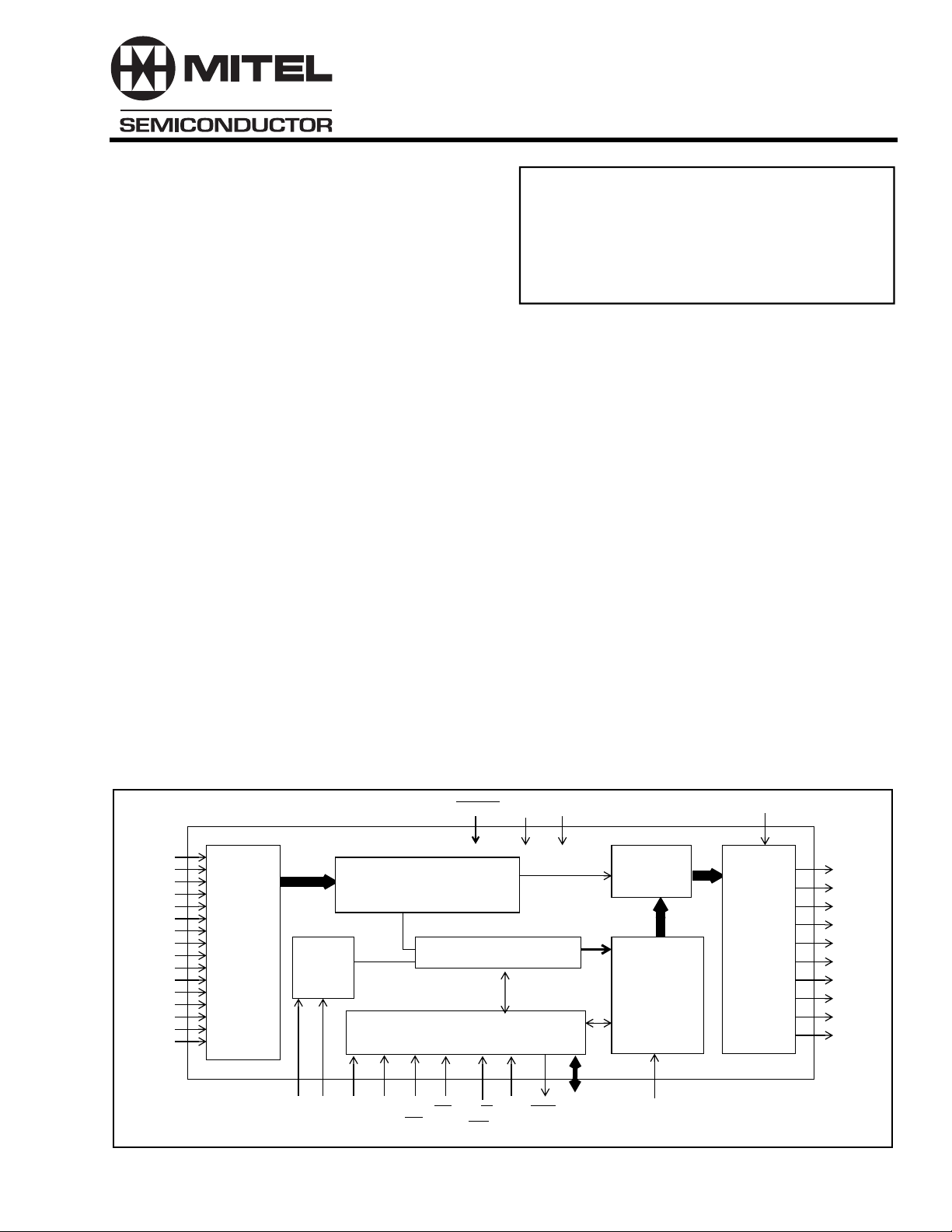
STi0
STi1
STi2
STi3
STi4
STi5
STi6
STi7
STi8
STi9
STi10
STi11
STi12
STi13
STi14
STi15
** for 48-pin SSOP only
Serial
to
Parallel
Converter
Timing
Unit
CLK FR AS/
ALE
**
VDDV
DTA
SS
AD7/
AD0
Output
Connection
Memory
RESET
Multiple Buffer Data
Memory
Internal Registers
Microprocessor
Interface
IM DS
RD
CS R/W
WR
A0/
A7
Figure 1 - Functional Block Diagram
MUX
CSTo
ODE
Parallel
to
Serial
Converter
STo0
STo1
STo2
STo3
STo4
STo5
STo6
STo7
STo8
STo9
1
Page 2
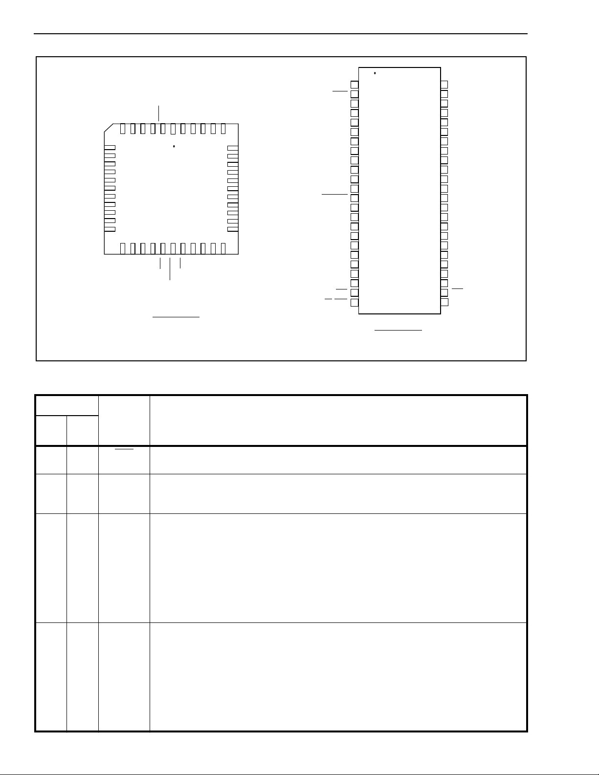
MT89L86 Advance Information
STi3
STi4
STi5
STi6/A6
STi7/A7
V
DD
FR
CLK
STi8/A0
STi9/A1
STi10/A2
AS/ALE
7
8
9
10
11
12
13
14
15
16
17
IM
STi0
STi1
STi2
STi11/A3
STi12/A4
STi13/A5
44 PIN PLCC
DTA
ODE
STo0
CS
W/WR
R/
AD7
STo1
AD6
CSTo
16 5 4 3 2 44434241
231819202122 242526 2728
RD
DS/
STo2
STi14/STo8
40
39
38
37
36
35
34
33
32
31
30
29
AD5
STi15/STo9
STo3
STo4
STo5
STo6/A6
STo7/A7
V
SS
AD0
AD1
AD2
AD3
AD4
V
DTA
STi0
STi1
STi2
AS/ALE
STi3
STi4
STi5
STi6/A6
STi7/A7
V
DD
RESET
FR
CLK
STi8/A0
STi9/A1
STi10/A2
IM
STi11/A3
STi12/A4
STi13/A5
DS/RD
R/W\WR
1
SS
2
3
4
5
6
7
8
9
10
11
12
13
14
15
16
17
18
19
20
21
22
23
24
48 PIN SSOP
(JEDEC MO-118, 300mil Wide)
48
47
46
45
44
43
42
41
40
39
38
37
36
35
34
33
32
31
30
29
28
27
26
25
CSTo
ODE
STo0
STo1
STo2
STi14/STo8
STo3
STo4
STo5
STo6/A6
STo7/A7
V
SS
V
DD
AD0
AD1
AD2
AD3
AD4
STi15/STo9
AD5
AD6
AD7
CS
V
SS
Figure 2 - Pin Connections
Pin Description
Pin #
44
PLCC48SSOP
22 DTA Data Acknowledgment (Open Drain Output). This active low output indicates that a
3-5
7-9
3-5
7-9
10 10 STi6/A6 ST-B US Input 6/Addr.6 input (5V-tolerant Input). The function of this pin is determined
11 11 STi7/A7 ST-B US Input 7/Addr.7 input (5V-tolerant Input): The function of this pin is determined
Name Description
data bus transfer is complete. A pull-up resistor is required at this output.
STi0-5 ST-BUS Inputs 0 to 5 (5V-tolerant Inputs). Serial data input streams. These streams
may have data rates of 2.048, 4.096 or 8.192 Mbit/s with 32, 64 or 128 channels,
respectively.
by the switching configuration enabled. If non-multiplexed CPU bus is used along with
a higher input rate of 8.192 or 4.096 Mb/s, this pin provides A6 address input function.
For 2.048 and 4.096 Mb/s (8x4) applications or when the multiplexed CPU bus
interface is selected, this pin assumes STi6 function. See Control Register bits
description and Tables 1, 2, 6 & 7 for more details.
Note that for applications where both A6 and STi6 inputs are required simultaneously
(e.g., 8 x 4 switching configuration at 4.096 Mb/s or rate conversion between 2.048Mb/
s to 4.196 or 8.192 Mb/s) the A6 input should be connected to pin STo6/A6.
by the switching configuration enabled. If non-multiplexed CPU bus is used along with
a higher input rate of 8.192 Mb/s, this pin provides A7 address input function.
For 2.048 and 4.096 Mb/s (8x4) applications or when the multiplexed CPU bus is
selected, this pin assumes STi7 function. See Control Register bits description and
Tables 1, 2, 6 & 7 for more details.
Note that for applications where both A7 and STi7 inputs are required simultaneously
(e.g., 2.048 to 8.192 Mb/s rate conversion) the A7 input should be connected to pin
STo7/A7.
2
Page 3
Advance Information MT89L86
Pin Description (continued)
Pin #
44
PLCC48SSOP
Name Description
12 12,36 V
+3.3 Volt Power Supply.
DD
13 RESET Device Reset ( 5v-tolerant input). This pin is only available for the 48-pin SSOP
package. In normal operation, This active low input puts the MT89L86 in its reset state .
It clears the internal counters and registers. All ST-BUS outputs are set to the high
impedance state. The RESET pin must be held low for a minimum of 100nsec to reset
the device.
13 14 FR Frame Pulse (5V-tolerant Input). This input accepts and automatically identifies frame
synchronization signals formatted according to ST-BUS and GCI interface
specifications.
14 15 CLK Clock (5V-tolerant Input). Serial clock for shifting data in/out on the serial streams.
Depending on the serial interface speed selected by IMS (Interface Mode Select)
register, the clock at this pin can be 4.096 or 8.192 MHz.
15-17 16-18 STi8/A0,
STi9/A1,
STi10/A2
Address 0-2 / Input Streams 8-10 (5V-tolerant Input). When the non-multiple xed CPU
bus is selected, these lines provide the A0-A2 address lines to the MT89L86 internal
registers. When the 16x8 switching configuration is selected, these pins are ST-BUS
serial inputs 8 to 10 receiving data at 2.048 Mb/s.
19-21 20-22 STi11/A3,
STi12/A4,
STi13/A5
Address 3-5 / Input Streams 11-13 (5V-tolerant Input). When the non-multiplexed
CPU bus is selected, these lines provide the A3-A5 address lines to the MT89L86
internal registers. When the 16x8 switching configuration is selected, these pins are
ST-BUS serial inputs 11 to 13 receiving data at 2.048 Mb/s.
22 23 DS/RD Data Strobe/Read (5V-tolerant Input). When the non-multiple x ed CPU b us or Motorola
multiplex ed b us is selected, this input is DS. This active high input works in conjunction
with CS to enable read and write operation.
For the Intel/National multiplexed bus interface, this input is RD. This active low input
configures the data bus lines (AD0-7) as outputs.
23 24 R/W\WR Read/Write \ Write (5V -tolerant Input). F or the non-multiple x ed or Motorola multiple x ed
bus interface, this input is R/W. This input controls the direction of the data bus lines
(AD0-AD7) during a microprocessor access.
For the Intel/National multiplexed bus interface, this input is WR. This active low signal
configures the data bus lines (AD0-7) as inputs.
24 26 CS Chip Select (5V-tolerant Input). This active low input enables a microprocessor read
or write of the MT89L86’s internal control register or memories.
25-27
29-33
27-29
31-35
AD7-AD0 Data Bus (Bidirectional): These pins provide microprocessor access to the internal
control registers, connection memories high and low and data memories. For the
multiplexed bus interface these pins also provide the input address to the internal
Address Latch circuit.
34 1,
V
SS
Ground.
25,37
35 38 STo7/A7 ST-BUS Output 7/Address 7 input (Three-state output/input). The function of this pin
is determined by the switching configuration enabled. If non-multiplexed CPU bus is
used along with data rates employing 8.192 Mb/s rates, this pin provides A7 address
input function. For 2.048 Mb/s applications or when the multiple x ed CPU bus interface
is selected, this pin assumes STo7 function. See Tables 1, 2, 6 & 7 for more details.
Note that for applications where A7 input and STo7 output are required simultaneously
(e.g., 8.192 to 2.048 Mb/s rate conversion), the A7 input should be connected to pin
STi7/A7.
3
Page 4
MT89L86 Advance Information
Pin Description (continued)
Pin #
44
PLCC48SSOP
36 39 STo6/A6 ST-BUS Output 6/Address 6 input (Three-state output/input). The function of this
37-39
41-43
40-42
44-46
44 47 ODE Output Drive Enable (5V -tolerant Input). This is the output enab le input for the STo0
1 48 CSTo Control ST-BUS Output (Output). This is a 2.048 Mb/s output containing 256 bits per
6 6 AS/ALE Address Strobe or Latch Enable (5V-tolerant Input). This input is only used if
18 19 IM CPU Interface Mode (5V-tolerant Input). If HIGH, this input configures the MT89L86
28 30 STi15/
40 43 STi14/
Name Description
pin is determined by the switching configuration enabled. If non-multiple x ed CPU bus is
used along with a higher data rate employing 8.192 or 4.096 Mb/s, this pin pro vides the
A6 address input function. For 2.048 Mb/s applications or when the multiplexed CPU
bus interface is selected, this pin assumes STo6 function. See Tables 1, 2, 6 & 7 for
more details.
Note that for applications where both A6 input and STo6 output are required
simultaneously (e.g., 4.096 to 2.048 Mb/s or 8.192 to 2.048 Mb/s rate conversion
applications), the A6 input should be connected to pin STi6/A6.
STo5-0 ST-BUS Outputs 5 to 0 (Three-state Outputs). Serial data output streams. These
serial streams may be composed of 32, 64 and 128 channels at data rates of 2.048,
4.096 or 8.192 Mbit/s, respectively.
to STo9 serial outputs. If this input is low STo0-9 are high impedance. If this input is
high each channel may still be set to high impedance by using per-channel control bits
in Connect Memory High.
frame. The level of each bit is determined by the CSTo bit in the Connect Memory high
locations.
multiplexed bus is selected via the IM input pin.
The falling edge of this signal is used to sample the address into the address latch
circuit. When the non-multiplexed bus interface is selected, this input is not required
and should be connected to ground.
in the multiplexed microprocessor bus mode. When this input pin is connected to
ground, the MT89L86 assumes non-multiplexed CPU interface.
ST-BUS Input 15 / ST -BUS Output 9 (Input/three-state output). This pin is only used
STo9
STo8
if multiplexed CPU bus is selected. If 16-input x 8-output switching configuration is
enabled in the SCB bits (IMS register), this pin is an input receiving serial ST-BUS
stream 15 at a data rate of 2.048 Mbit/s.
If Stream Pair Selection capability is enabled (see s witching configur ation section), this
pin is the ST-BUS stream 9 output.
When non-multiplexed bus structure is used, this pin should be connected to ground.
ST-BUS Input 14 / ST -BUS Output 8(Input/three-state output). This pin is only used
if multiplexed CPU bus is selected. If 16-input x 8-output switching configuration is
enabled in the SCB bits (IMS register), this pin is an input that receives serial ST-BUS
stream 14 at a data rate of 2.048 Mbit/s.
If Stream Pair Selection capability is enabled (see s witching configuration section), this
pin is the ST-BUS stream 8 output.
When non-multiplexed bus structure is used, this pin should be connected to ground.
4
Page 5

Advance Information MT89L86
Device Overview
With the integration of voice, video and data services
in the same network, there has been an increasing
demand for systems which ensure that data at N x 64
kb/s rates maintain sequence integrity while being
transported through time-slot interchange circuits.
This requirement demands time-slot interchange
devices which perform switching with constant
throughput delay for wideband data applications
while maintaining minimum delay for voice channels.
The MT89L86 device meets the above requirement
and allows existing systems based on the MT8980D
to be easily upgraded to maintain the data integrity
when wideband data is transported. The device is
designed to switch 32, 64 or N x 64 bit/s data. This
MT89L86 can provide frame integrity for data
applications and minimum throughput switching
delay for voice applications on a per channel basis.
The serial streams of the MT89L86 can operate at
2.048, 4.096 or 8.192 Bit/s and are arranged in 125
µs wide frames which contain 32, 64 and 128
channels, respectively. In addition, a built-in rate
conversion circuit allows the user to interconnect
various backbone speeds like 2.048 or 4.096 or
8.192 Mb/s while maintaining the control of
throughput delay function on a per-channel basis.
By using Mitel Message mode capability, the
microprocessor can access input and output timeslots on a per channel basis to control external
circuits or other ST-BUS devices. This MT89L86
automatically identifies the polarity of the frame
synchronization input signal and configures its serial
port to be compatible to both ST-BUS and GCI
formats.
Two different microprocessor bus interfaces can be
selected through an input mode pin (IM): NonMultiplexed or Multiplexed. These interfaces provide
compatibility with Intel/National multiplexed and
Motorola Multiplexed/Non-Multiplexed buses. The
MT89L86 provides a 16 x 8 switching configuration
to form a 512 x 256 channel blocking matrix. Also, a
flexible Stream Pair Selection operation allows the
software selection of which pair of input and output
streams can be connected to an internal 128 x 128
matrix. See Switching Configurations section for
details.
TDM serial data can be received at different rates
and from different number of serial streams.
Data and Connect Memories
For all data rates, the received serial data is
converted to parallel format by the serial to parallel
converters and stored sequentially in a Data
Memory. Depending on the selected operation
programmed in the IMS (Interface Mode Select)
register, the Data Memory may have up to 512 bytes
in use. The sequential addressing of the Data
Memory is performed by an internal counter which is
reset by the input 8 kHz frame pulse (FR) marking
the frame boundaries of the incoming serial data
streams.
Data to be output on the serial streams may come
from two sources: Data Memory or Connect Memory.
Locations in the Connect Memory, which is split into
HIGH and LOW parts, are associated with particular
ST-BUS output streams. When a channel is due to
be transmitted on an ST-BUS output, the data for the
channel can either be switched from an ST-BUS
input as in connection mode or it can be from the
Connect Memory Low as in message mode. Data
destined for a particular channel on the serial output
stream is read from the Data Memory or Connect
Memory Low during the previous channel time-slot.
This allows enough time for memory access and
parallel to serial conversion.
Connection and Message Modes
In the connection mode, the addresses of the input
source data for all output channels are stored in the
Connect memories High (CMH) and Low (CML). The
CML and CMH are mapped so that each location
corresponds to an output channel on the output
streams. The number of source address bits in CMH
and CML to be utilized varies according to the
switching configuration selected in the IMS register.
For details on the use of the source address data
(CAB and SAB bits), see CMH and CML bit describethin (Figures 5 & 6). Once the source address bits
are programmed by the CPU, the contents of the
Data Memory at the selected address are transferred
to the parallel-to-serial converters. By having the
output channel specify the source channel through
the connect memory, the user can route the same
input channel to several output channels, allowing
broadcast facility within the switch.
Functional Description
A functional Block Diagram of the 3.3V MT89L86 is
shown in Figure 1. Depending on the application,
In the message mode the CPU writes data to the
Connect Memory Low locations corresponding to the
output link and channel number. The contents of the
Connect Memory Low are transferred directly to the
parallel-to-serial converter one channel before it is to
5
Page 6

MT89L86 Advance Information
be output. The Connect Memory Low data is
transmitted on to the output every frame until it is
changed by the CPU with a new data.
The features of each output channel in the 3.3V
MT89L86 are controlled by the Connect Memory
High bits. These bits determine individual output
channels to be in message or connection mode,
select throughput delay types and enable/disable
output drivers. The Connect Memory High also
provides additional stream and channel address bits
for some configurations. In addition, the Connect
Memory High provides one bit to allow the user to
control the CST output in 2.048 Mb/s applications.
If an output channel is set to high-impedance, the
TDM serial stream output will be placed in high
impedance during that channel time. In addition to
the per-channel control, all channels on the TDM
outputs can be placed in high impedance by pulling
the ODE input pin LOW. This overrides the individual
per-channel programming by the Connect Memory
High bits.
The Connect Memory data is received via the
Microprocessor Interface through the data I/O lines.
The addressing of the MT89L86 internal registers,
Data and Connect memories is performed through
address input pins and some bits of the device's
Control register. The higher order address bits come
from the Control register, which may be written or
read through the microprocessor interface. The low er
order address bits come directly from address input
pins. For details on the device addressing, see
Software Control and Control register bits
description (Figure 3 & Tables 5, 6 and 7).
the IMS register. When Identical I/O data rates are
selected by the DMO bit, the switching configuration
and the number of the device's input and output
streams can be selected through the SCB bits
(Switching Configuration Bits) in the IMS register.
See Switching Configurations section for details.
Depending on the application, the interface clock can
be selected to be twice the data rate or equal to the
data rate. This selection is performed through bit
CLKM in the IMS register. For applications where
both serial inputs and outputs are at 2.048 Mb/s (STBUS or GCI format), the CLKM bit should be set
LOW enabling the interface clock to be twice the bit
rate. In applications where both inputs and outputs
are at 4.096 or 8.192 Mb/s, CLKM should be set
HIGH enabling the interface clock to be equal to the
bit rate. In applications where inputs and outputs are
at different rates, the CLKM bit has no effect.
In applications with serial links at 2.048 Mb/s (see
Figures 15 to 18), the input 8 kHz frame pulse can be
in either ST-BUS or GCI format. This MT89L86
automatically detects the presence of an input frame
pulse and identifies what type of backbone is present
on the serial interface. Upon determining the
interface connected to the serial port, the internal
timing unit establishes the appropriate transmit and
sampling edges. In ST-BUS format, every second
falling edge of the 4.096 MHz clock marks a bit
boundary and the input data is clocked in by the
rising edge, three quarters of the way into the bit cell.
In GCI format, every second rising edge of the 4.096
MHz clock marks the bit boundary while data
sampling is performed during the falling edge, at
three quarters of the bit boundaries.
Serial Data Interface
The master clock (CLK) can be either at 4.096 or
8.192 MHz allowing serial data link operations at
2.048, 4.096 and 8.192 Mb/s. These data rates can
be independently selected on input and output
streams allowing this MT89L86 device to be used in
various speed backbones and in rate conversion
applications. The selected data rates apply to the
inputs or the output streams. Different bit rates
among input streams or among output streams are
not allowed. Due to the I/O data rate selection
flexibility, two major operations can be selected:
Identical or Different I/O data rates.
The DMO bit (Device Main Operation) in the IMS
register is used for selecting between Identical I/O
rates or Different I/O rates. On system power-up, the
CPU should set up the DMO, the IDR (Input Data
Rate) and ODR (Output Data Rate) bits located in
6
For identical I/O rates at 4.096 and 8.192 Mb/s (see
Figure 19), the clock and interface data rates are
equal. The bit transmit and sampling edges vary
according to the applied frame pulse polarity. For
example, if the FR pulse polarity is positive, the bit
transmit operation is done on every rising edge of
CLK and the bit sampling on every falling edge. If
the FR pulse polarity is negative, these edges are
inverted. For different I/O rates, the MT89L86 side
operating at 2.048 Mb/s data rate will comply with
ST-BUS or GCI interfaces for transmit and sampling
procedures. The MT89L86 side operating at 4.096 or
8.192 Mb/s behaves according to the frame pulse
polarity applied. See Figures 21 to 24.
Switching Configurations
Switching configurations are determined basically by
the interface rates selected at the serial inputs and
outputs. To specify the switching configuration
Page 7

Advance Information MT89L86
required, the IMS register has to be initialized on
system power-up. In case of Identical I/O r ates (DMO
bit LOW) at both inputs and outputs, the switching
configuration is selected by the two SCB bits as
shown in Table 8 (see IMS register). In case of
different I/O rates (DMO bit HIGH), the switching
configuration is always non-blocking with different
number of I/O streams which is defined by the IDR
and ODR bits (see IMS register).
Identical Input/Output Data Rates
When identical input/output data rate is selected by
the DMO bit, the I/O rate is determined by the IDR01 bits, and the ODR0-1 bits are ignored. For each
data rate specified by the IDR bits, diff erent switching
configurations can be selected in the SCB1-0 bits.
Serial Links with Data Rates at 2.048 Mb/s
When the 2.048 Mb/s data rate is selected at the IDR
bits, four different I/O configurations can be selected
by the SCB1-0 bits (see Table 8); 8 x 8, 16 x 8, 4 x 4
with stream pair selection and nibble switching.
If 8 x 8 switching configuration is selected, a 256 x
256 channel non-blocking switching matrix is
available. In this configuration, the 3.3V MT89L86 is
configured with 8 input and 8 output data streams
with 32 64 Bit/s channels each. The interface clock
for this operation is 4.096 MHz with both ST-BUS and
GCI compatibilities and the per-channel selection
between variable and constant throughput delay
functions is provided.
In 16 x 8 switching configuration, a 512 x 256
channel blocking switch matrix is available. This
configuration is available only when the CPU bus
interface is configured in the multiplexed mode. The
device clock in this application is 4.096 MHz, STBUS or GCI compatible. This configuration only
provides variable throughput delay.
If the stream pair selection switching configuration is
selected, only four input and four outputs (4 pairs of
serial streams) can be selected by the CPU to be
internally connected to the switch matrix, totalling a
128 x 128 channel non-blocking switch. From the 10
serial link pairs available, two pairs are permanently
connected to the internal matrix (STi0/STo0 and
STi1/STo1). An internal stream pair selection
capability allows two additional pairs of serial links to
be selected from the remaining 8 pairs (from STi/
STo2 to STi9/STo9) and be connected to the internal
matrix along with the permanently connected STi0/
STo0 and STi1/STo1 streams. The two additional
pair of streams called stream pair A and stream pair
B, should be selected in the Stream Pair Selection
register (SPS). The device clock for this operation is
4.096 MHz compatible to ST-BUS and GCI
interfaces. In addition, the per-channel selection
between variable or constant throughput delay is
available.
In the nibble switching configuration, 4-bit wide 32
Kb/s data channels can be switched within the
device. Every serial stream is run at 2.048 Mb/s and
transports 64 nibbles per frame. When the Nibble
Switching is selected at SCB bits, the 3.3V MT89L86
automatically assumes a 8-input x 4-output stream
configuration, providing a blocking switch matrix of
512 x 256 nibbles. If a non-blocking switch matrix is
required for nibble switching, the switch capacity is
reduced to 256 x 256 channel with a 4 input x 4
output configuration; the non-blocking matrix can be
arranged by the user by selecting any four of the 8
input streams. In nibble switching the interface clock
is 4.096 MHz.
Serial Links with Data Rates at 4.096 Mb/s
Two I/O configurations can be enabled by the SCB
bits when input and output data rates are 4.096 Mb/s
on each serial stream: 8 x 4 and 4 x 4. When 8 x 4
switching configuration is selected, a 512 x 256
channel blocking switch is available with serial
streams carrying 64, 64 Kb/s channels each. For this
operation, a 4.096 MHz interface clock equal to the
bit rate should be provided to the 3.3V MT89L86.
Only variable throughput delay mode is provided.
In the 4 x 4 switching configuration, a 256 x 256
channel non-blocking switch is available with serial
streams carrying 64, 64 Kb/s channels each. In this
configuration, the interface clock is 4.096 MHz and
the per-channel selection between variable and
constant throughput delay operation is provided.
Figure 19 shows the timing for 4.096 Mb/s operation.
Serial Links with Data Rates at 8.192 Mb/s
Only 2 input x 2 output stream configuration is
available for 8.192 Mb/s, allowing a 256 x 256
channel non-blocking switch matrix to be
implemented. To enable this operation, the IDR bits
should be programmed to select 8.192 Mb/s rates
and the SCB bits have no effect. At 8.192 Mb/s,
every input and output stream provides 128 timeslots per frame. The interface clock for this operation
should be 8.192 MHz. Figure 19 shows the timing for
8.192 Mb/s operation.
Table 1 summarizes the 3.3V MT89L86 switching
configurations for identical I/O data rates.
7
Page 8
MT89L86 Advance Information
Interface
Serial
Interface
Data Rate
2 Mb/s 4.096 8x8 256x256 Non-Blocking STi0-7/STo0-7 Yes
2 Mb/s 4.096 16x8 512x256 Blocking STi0-15/STo0-7 No
2 Mb/s 4.096 10x10 128x128 Non-Blocking
Nibble
Switching
(2 Mb/s)
4 Mb/s 4.096 8x4 512x256 Blocking STi0-7/STo0-3 No
4 Mb/s 4.096 4x4 256x256 Non-Blocking STi0-3/STo0-3 Yes
8 Mb/s 8.192 2x2 256x256 Non-Blocking STi0-1/STo0-1 Yes
Different Input/Output Data Rates
When Different I/O rate is selected by the DMO bit,
the input and output data rates should be selected at
the IDR and ODR bits, respectively. The Switching
Configuration Bits (SCB) are ignored with this
operation. This selection allows the user to multiplex
conventional 2.048 Mb/s serial streams into two
higher rates and vice-versa. In addition to the rate
conversion itself, the MT89L86 allows for a complete
256 x 256 channel non-blocking switch at different
rates. In this operation, the per-channel variable/
constant throughput delay selection is provided.
Depending on which data rates are programmed for
input and output streams, the number of data
streams used on the input and output as well as the
serial interface clock (CLK input pin) is different.
Once the CPU defines the data rates at the IDR and
ODR bits, the MT89L86 automatically configures
itself with the appropriate number of input and output
Clock
required at
CLK Pin
(MHz)
4.096 8x4 512x256 Nibbles STi0-7/STo0-3 No
Table 1 - Switching Configurations for Identical Input and Output Data Rate
Number of
Input x
Output
Streams
Matrix
Channel
Capacity
(only 4-input x 4-output
can be selected)
streams for the desired operation. Table 2
summarizes the four options available when it is
used with different I/O rates. Figures 21 to 24 show
the timing for each of the four modes shown in Table
2.
Input Frame Offset Selection
For the 4.096 and 8.192 Mb/s serial interface data
rates, the MT89L86 provides a feature called Input
Frame Offset allo wing the user to compensate for the
varying delays at the incoming serial inputs while
building large switch matrices. Usually, different
delays occur on the digital backbones causing the
data and frame synchronization signals to be skewed
at the input of the switch device. This may result in
the system frame synchronization pulse to be active
at the MT89L86’s FR input before the first bit of the
frame is received at the serial inputs.
Input/Output
Streams Used
STi0-9/STo0-9 Yes
Variable/
Constant
throughput
Delay
Selection
Interface
Input and
Output
Data Rates
2 Mb/s to 4 Mb/s 4.096 8x4 256x256 Non-Blocking STi0-7/STo0-3 Yes
2 Mb/s to 8 Mb/s 8.192 8x2 256x256 Non-Blocking STi0-7/STo0-1 Yes
4 Mb/s to 2 Mb/s 4.096 4x8 256x256 Non-Blocking STi0-3/STo0-7 Yes
8 Mb/s to 2 Mb/s 8.192 2x8 256x256 Non-Blocking STi0-1/STo0-7 Yes
8
Clock
required at
CLK Pin
(MHz)
Table 2 - Switching Configurations for Different I/O Data Rates
Number
of Input
x Output
Streams
Matrix
Channel Capacity
Input/Output
Streams Used
Variab le/
Constant
throughput
Selection
Delay
Page 9
Advance Information MT89L86
When the input frame offset is enabled, an "internal
delay" of up to four clock periods is added to the
actual data input sampling, providing the MT89L86
serial timing unit a new input frame reference. An
internal virtual frame is created which is aligned with
the framing of the actual serial data coming in at the
serial inputs and not with the FR frame pulse input.
In this operation, the transmission of the output
frame on the serial links is still aligned to the frame
pulse input signal (FR).
The selection of the data input sampling delay is
defined by the CPU in the Frame Input Offset
Register (FIO). If this function is not required in the
user's applications, the FIO register should be set up
during system initialization to a state where offset
functions are disabled.
Delay Through the MT89L86
The switching of information from the input serial
streams to the output serial streams results in a
delay. Depending on the type of information to be
switched, this MT89L86 can be programmed to
perform time-slot interchange functions with different
throughput delay capabilities on a per-channel basis.
For voice applications, variable throughput delay can
be selected ensuring minimum delay between input
and output data. In wideband data applications,
constant throughput delay can be selected
maintaining the frame integrity of the information
through the switch.
The delay through the device varies according to the
type of throughput delay selected in the V/C bit of the
connect memory high.
Variable Throughput Delay Mode (V/C bit = 0)
Identical I/O Data Rates
The delay in this mode is dependent on the
combination of source and destination channels and
it is independent of the input and output streams.
The minimum delay achievable in this MT89L86
depends on the data rate selected for the serial
streams. For instance, for the 2.048 Mb/s data rate,
the minimum delay achieved corresponds to three
time-slots. For the 4.096 Mb/s data rate it
corresponds to five time-slots while it is nine timeslots for the 8.192 Mb/s data rate. Switching
Output Channel (# m)
Input Rate
m < n m=n, n+1, n+2 m= n+3, n+4 m=n+5, .. n+8 m > n+8
2.048 Mb/s 32-(n-m) t.s. m-n + 32 t.s. m-n t.s. m-n t.s. m-n t.s.
4.096 Mb/s 64-(n-m) t.s. m-n + 64 t.s. m-n+64 t.s. m-n t.s. m-n t.s.
8.192 Mb/s 128-(n-m) t.s. m-n + 128 t.s. m-n+128 t.s. m-n+128 t.s. m-n t.s.
Table 3a - Variable Throughput Delay Values for Identical I/O Rate Applications
n= input channel, t.s. = time-slot
I/O Data Rate
Configuration
2 Mb/s to 4 Mb/s
2 Mb/s to 8 Mb/s
4 Mb/s to 2 Mb/s
8 Mb/s to 2 Mb/s
0, 1 2, 3 4, 5 6, 7
dmin=5x 4Mb/s t.s.
dmax=1 fr.+(4x 4Mb/s t.s.)
dmin=9x 8Mb/s t.s.
dmax=1 fr.+(8x 8Mb/s t.s.)
dmin=3x 2Mb/s t.s.
dmax=1 fr.+(2x 2Mb/s t.s.)
dmin=3x 2Mb/s t.s.
dmax=1 fr.+(2x 2Mb/s
t.s.)
dmin=(2x 2Mb/s t.s.)+
(3x 8Mb/s t.s.)
dmax=1 fr.+(1x 2Mb/s
t.s.)+(3x 8Mb/s t.s.)
Output Stream Used
dmin=(2x 2Mb/s t.s.)+(1x 4Mb/s t.s.)
dmax=1 fr.+(1x 2Mb/s t.s.)+(1x 4Mb/s t.s.)
dmin=(2x 2Mb/s t.s.)+
(2x 8Mb/s t.s.)
dmax=1 fr.+(1x 2Mb/s
t.s.)+(2x 8Mb/s t.s.)
dmin=(2x 2Mb/s t.s.)+
(1x 8Mb/s t.s.)
dmax=1 fr.+(1x 2Mb/s
t.s.)+(1x 8Mb/s t.s.)
Table 3b - Min/Max Throughput Delay Values for Different I/O Rate Applications
Notes: dmin and dmax are measured in time-slots and at the point in time when the output channel is completely shifted out.
t.s. = time-slot
fr. = 125 µs frame
2 Mb/s t.s. = 3.9 µs
4 Mb/s t.s. = 1.95 µs
8 Mb/s t.s. = 0.975 µs
9
Page 10
MT89L86 Advance Information
Data Rate Throughput Delay (d)
2.048 Mb/s d=[32 + (32 - IN) + (OUT - 1)]; (expressed in # time-slots)
2.048 Mb/s time-slot: 3.9µs
IN: input time-slot (from 1 to 32)
OUT: output time-slot (from 1 to 32)
4.096 Mb/s d=[64 + (64 - IN) + (OUT - 1)]; (expressed in # time-slots)
4.096 Mb/s time-slot: 1.95 µs
IN: input time-slot (from 1 to 64)
OUT: output time-slot (from 1 to 64)
8.192 Mb/s d=[128 + (128 - IN) + (OUT - 1)]; (expressed in # time-slots)
8.192 Mb/s time-slot: 0.975 µs
IN: input time-slot (from 1 to 128)
OUT: output time-slot (from 1 to 128)
Table 4 - Constant Throughput Delay values
configurations with input and output channels that
provides more than its corresponding minimum
throughput delay, will have a throughput delay equal
to the difference between the output and input
channels; i.e., the throughput delay will be less than
one frame period. Table 3a shows the throughput
delay for each data rate operation.
Different I/O Data Rates
Except for the 2 Mb/s to 4 Mb/s and the 2 Mb/s to 8
Mb/s rate conversion operations, the throughput
delay from the MT89L86 may vary according to the
output stream used for switching.
Table 3b explains the worst case conditions for the
throughput delay when different I/O data rate
switching configurations are used.
Constant Throughput Delay mode (V/C bit = 1)
In this mode frame sequence integrity is maintained
in both Identical and Different I/O Data Rate
operations by making use of a multiple Data-Memory
buffer technique. The input channels written in any of
the buffers during frame N will be read out during
frame N+2. In applications at 2.048 Mb/s for
instance, the minimum throughput delay achievable
in constant delay mode will be 32 time-slots; for
example, when input time-slot 32 (channel 31) is
switched to output time-slot 1 (channel 0). Likewise,
the maximum delay is achieved when the first time
slot in a frame (channel 0) is switched to the last
time-slot in the frame (channel 31), resulting in 94
time-slots of delay.
To summarize, any input time-slot from input frame N
will always be switched to the destination time-slot
on output frame N+2. Table 4 describes the constant
throughput delay values at different data rates.
Microprocessor Port
The non-multiplexed bus interface provided by the
MT89L86 is identical to that provided in the MT8986
Digital Switch device. In addition to the nonmultiplexed bus, this 3.3V MT89L86 device provides
an enhanced microprocessor interface with
multiplexed bus structure compatible to both
Motorola and Intel buses. The multiplexed bus
structure is selected by the CPU Interface Mode (IM)
input pin.
If the IM input pin is connected to ground, the
MT89L86’s parallel port assumes its default Motorola
non-multiplexed bus mode identical to that of
MT8986. If the IM input is connected HIGH, the
internal parallel microprocessor port provides
compatibility to MOTEL (MOtorola and InTEL
compatible bus) interface allowing direct connection
to Intel, National and Motorola CPUs.
The on-chip MOTEL circuit automatically identifies
the type of CPU Bus connected to the device. This
circuit uses the level of the DS/RD input pin at the
rising edge of the AS/ALE to identify the appropriate
bus timing connected to the MT89L86. If DS/RD is
LOW at the rising edge of AS/ALE then the Motorola
bus timing is selected. If DS/RD is HIGH at the rising
edge of AS/ALE, the Intel bus timing is selected.
When the parallel port of this device is operating in
Motorola, National or Intel multiplexed bus
interfaces, the signals available for controlling the
device are: AD0-AD7 (Data and Address), ALE/AS
(Address Latch Enable/Address Strobe), DS/RD
(Data Strobe/Read), R/W\WR (Read/Write\Write),
CS (Chip Select) and DTA (Data Acknowledgment).
In the Motorola non-multiplexed bus mode, the
interface control signals are: data bus (AD0-AD7),
10
Page 11
Advance Information MT89L86
six address input lines (A0-A5) and four control lines
(CS , DS, R/W and DTA). See Figures 25 to 27 for
each CPU interface timing.
The parallel microprocessor port provides the access
to the IMS, Control registers, the Connection
Memory High, the Connection Memory Low and the
Data Memory. All locations can be read or written
except for the data memory which can be read only.
Software Control
The address bus on the microprocessor interface
selects the internal registers and memories of the
MT89L86. If the A5 address input is LOW, the
Internal Control, Interface Mode, Stream Pair
Selection and Frame Input Offset registers are
addressed by the A4 to A0 bits according to Table 5.
If the A5 input is HIGH, the remaining address input
lines are used to select memory subsections of up to
128 locations corresponding to the maximum
number of channels per input or output stream. The
address input lines and the Stream Address bits
(STA) of the Control register give the user the
capability of accessing all sections of the MT89L86’s
Data and Connect memories.
The Control and Interface Mode Selection registers
together control all the major functions of the device.
The Interface Mode Select register should be set up
during system power-up to establish the desired
switching configuration as explained in the Serial
Interface and Switching Configurations sections.
The Control register is dynamically used by the CPU
to control switching operations in the MT89L86. The
Control register selects the device's internal
memories and its subsections to specify the input
and output channels selected for switching
procedures.
The data in the Control register consists of Split
memory and Message mode bits, Memory select and
Stream Address bits. The memory select bits allow
the Connect Memory HIGH or LOW or the Data
Memory to be chosen, and the Stream Address bits
define an internal memory subsections
corresponding to input or output ST-BUS streams.
Bit 7 (Slip Memory) of the Control register allows
split memory operation whereby reads are from the
Data memory and writes are to the Connect Memor y
LOW.
The Message Enable bit (bit 6) places every output
channel on every output stream in message mode;
i.e., the contents of the Connect Memory LOW
A7 A6 A5 A4 A3 A2 A1 A0 Location
X X 0 0 0 0 0 0 Control Register
X X 0 0 0 0 0 1 Interface Mode Select Register
X X 0 0 0 0 1 0 Stream Pair Select Register
X X 0 0 0 0 1 1 Frame Input Offset Register
0 0 1 0 0 0 0 0 Channel 0*
0
•
•
0
0
•
•
0
1
1
1
1
0
•
•
1
0
•
•
1
0
•
•
1
0
•
•
1
1
•
•
1
Channel 1*
•
•
Channel 31*
0 1 1 0 0 0 0 0 Channel 32**
0
•
•
0
1
•
•
1
1
•
•
1
0
•
•
1
1
1
1
1
1
1
1
1
0
•
•
1
0
•
•
1
0
•
•
1
0
•
•
1
0
•
•
1
0
•
•
1
0
•
•
1
0
•
•
1
1
•
•
1
0
•
•
1
Channel 33**
•
•
Channel 63**
Channel 64***
•
•
Channel 127***
Table 5 - Address Memory Map
*: channels 0 to 31 are used in 2.048 Mb/s (8 x 8, 16 x 8 and 10 x 10)
**: channels 0 to 63 are used in 4.096 Mb/s (Nibble Switching, 4 x 4, 8 x 4 or Different I/O rates)
***: channels 0 to 127 are used in 8.192 Mb/s (2 x 2 or Different I/O rates)
11
Page 12

MT89L86 Advance Information
(CML) are output on the ST-BUS output streams
once every frame unless the ODE input pin is LOW.
If ME bit is HIGH, then the MT89L86 behaves as if
bits 2 (Message Channel) and 0 (Output Enable) of
every Connect Memory HIGH (CMH) locations were
set to HIGH, regardless of the actual value. If ME bit
is LOW, then bit 2 and 0 of each Connect Memor y
HIGH location function normally. For example, if bit 2
of the CMH is HIGH, the associated ST-BUS output
channel is in Message mode. If bit 2 of the CMH is
LOW, then the contents of the SAB and CAB bits of
the CMH and CML define the source information
(stream and channel) of the time-slot that is to be
switched to an output.
If the ODE input pin is LOW, then all ser ial outputs
are set to high impedance. If ODE is HIGH, then bit 0
(Output Enable) of the CMH location enables (if
HIGH) or disables (if LOW) the output drivers for the
corresponding individual ST-BUS output stream and
channel.
The contents of bit 1 (CSTo bit) of each Connection
Memory High location is output to the CSTo pin
once every frame. The CSTo pin is a 2048 Mbit/s
output which carries 256 bits. If CSTo bit is set HIGH,
the corresponding bit on CSTo output is transmitted
HIGH. If CSTo bit is LOW, the corresponding bit on
the CSTo output is transmitted LOW. The contents of
the 256 CSTo bits of the CMH are transmitted
sequentially to the CSTo output pin and are
synchronous to the 2.048 Mb/s ST-BUS streams. To
allow for delay in any external control circuitry the
contents of the CSTo bit is output one channel before
the corresponding channel on the ST-BUS streams.
For example, the contents of CSTo bit in position 0
(ST0, CH0) of the CMH, is transmitted
synchronously with ST-BUS channel 31, bit 7. The
contents of CSTo bit in position 32 (ST1, CH0) of the
CMH is transmitted during ST-BUS channel 31 bit 6.
For more detailed description of the CSTo operation,
see section 6 of Application Note MSAN-123.
During the microprocessor initialization routine, the
microprocessor should program the desired active
paths through the matrices, and put all other
channels into the high impedance state. Care
should be taken that no two ST-BUS outputs drive
the bus simultaneously. When this process is
complete, the microprocessor controlling the
matrices can bring the ODE signal high to relinquish
the high impedance state control to the OE bit of the
CMH (CMH
A RESET pin is available for the 48-pin SSOP
package. When this pin is set low for a minimum of
100n sec, the ST-BUS outputs are put to the high
impedance state and all register contents are set to
zero.
0s).
b
The V/C bit (Variable/Constant Delay) of each
Connect Memory High location allows the perchannel selection between Variable and Constant
throughput delay modes.
Initialization of the MT89L86
On initialization or power up, the contents of the
Connection Memory High can be in any state. This
is a potentially hazardous condition when multiple
MT89L86 ST-BUS outputs are tied together to form
matrices, as these outputs may conflict. The ODE
pin should be held low on power up to keep all
outputs in the high impedance condition.
12
Page 13

Advance Information MT89L86
Control Register - Read/Write
76543210
SM ME STA3 MS1 MS0 STA2 STA1 STA0
Bit Name Description
7SMSplit Memory . When 1, all subsequent reads are from the Data Memory and writes are to
the Connection Memory Low, except when the Control Register is accessed again. When
0, the Memory Select bits specify the memory for subsequent operations. In either case,
the Stream Address Bits select the subsection of the memory which is made available.
6MEMessage Enable. When 1, the contents of the Connection Memory Low are output on the
Serial Output streams except when in High Impedance as set by the ODE input. When 0,
the Connection Memory bits for each channel determine the output of the serial streams.
5STA3Stream Address Bit 3. When the 16 x 8 switching configuration is selected, this pin is
used with STA2-0 to select one of the 16 input data streams whenever the Data Memory is
to be read. The programming of this bit has no effect in other switching configurations.
4-3 MS1-0 Memory Select Bits. The memory select bits operate as follows:
0-0 - Not to be used
0-1 - Data Memory (read only from the CPU)
1-0 - Connection Memory Low
1-1 - Connection Memory High
2-0 STA2-0 The number expressed in binary notation on these bits refers to the input or output ST-BUS
stream which corresponds to the subsection of memory made accessible for subsequent
operations.
The use of these bits depends on the switching configuration as well as the device’s main
operation defined by the DMO bit of the Interface Mode Selection register. Tables 6 and 7
show the utilization of these bits according to the device’s main operation.
Figure 3 - Control Register Description
13
Page 14

MT89L86 Advance Information
Identical
I/O
Rate
2 Mb/s 8x8 STA2, STA1, STA0 STA2, STA1, STA0 A4, A3, A2, A1, A0
2 Mb/s 4x4 STA1, STA0 STA1, STA0 A4, A3, A2, A1, A0
2 Mb/s 16x8 STA3, STA2, STA1,
4 Mb/s 4x4 STA1, STA0 STA1, STA0 A6, A4, A3, A2, A1, A0
4 Mb/s 8x4 STA2, STA1, STA0 STA1, STA0 A6, A4, A3, A2, A1, A0
8 Mb/s 2x2 STA0 STA0 A7, A6, A4, A3, A2, A1, A0
Nibble Switch
(2 Mb/s)
* - for Data Memory Read operations A0 is not required since two nibbles are provided per read access.
# of Input x
Output
Streams
8x4 STA2, STA1, STA0 STA1, STA0 A6, A4, A3, A2, A1, A0 *
Table 6 - Use of STA Bits for Identical I/O Data Rate Operation
STA bits used to
select subsections
of the Data
Memory
STA0
STA bits used to
select
subsections of the
Connection
Memory
STA2, STA1, STA0 A4, A3, A2, A1, A0
Input Address pins used to
select individual
Connection and Data
Memory positions within the
selected subsection
Different
I/O
Rate
2 Mb/s to
4 Mb/s
2 Mb/s to
8 Mb/s
4 Mb/s to
2 Mb/s
8 Mb/s to
2 Mb/s
Note:In rate conversion applications, Data Memory subsections have different sizes than Connection Memory subsections. This
implies that different address inputs are used to select individual positions within the subsections for each type of memory.
Input x
Output
Streams
Config.
8x4 STA2, STA1,
8x2 STA2, STA1,
4x8 STA1, STA0 STA2, STA1,
2x8 STA0 STA2, STA1,
STA bits used
to select
Data
Memory
subsections
STA0
STA0
Table 7 - Use of STA Bits for Different I/O Data Rate Operation
STA bits used
to select
Connection
Memory
subsections
STA1, STA0 A4, A3, A2, A1, A0 A6,A4, A3, A2, A1, A0
STA0 A4, A3, A2, A1, A0 A7, A6, A4, A3, A2, A1,
STA0
STA0
Input Address pins used
to access individual
Data Memory
positions within the
selected subsection
A6, A4, A3, A2, A1, A0 A4, A3, A2, A1, A0
A7, A6, A4, A3, A2, A1,A0A4, A3, A2, A1, A0
Input Address pins used
to access individual
Connection Memory
positions within the
selected subsection
A0
14
Page 15

Advance Information MT89L86
Interface Mode Selection Register - Read/Write
76543210
DMO IDR1 IDR0 ODR1 ODR0 SCB1 SCB0 CLKM
Bit Name Description
7 DMO Device Main Operation. This bit is used by the CPU to define one of the two main
operations of the 3.3V MT89L86. If this bit is LOW, the MT89L86 is configured for
identical I/O data rates. For this operation, the user should also specify the switching
configuration through the SCB bits.
If this bit is HIGH, the MT89L86 is configured in Different I/O data rate. This allows
combinations of input and output data rates as shown in Table 2. The SCB bits have no
effect in this application and the device is in Non-Bloc king s witch configur ation with a 256
x 256 channel capacity.
6-5 IDR1-0 Input Data Rate Selection. These two bits select three different data rates for the inputs
of the MT89L86. In the case of identical I/O rates (DMO bit = 0), these bits also
determine the serial output data rate.
IDR1 IDR0 Input Rate
0 0 2.048 Mb/s
0 1 4.096 Mb/s
1 0 8.192 Mb/s
1 1 reserved
4-3 ODR1-0 Output Data Rate Selection. These bits are only used when Different I/O rates are
selected (DMO bit=1). These two bits select three different data rates for the serial
outputs of the MT89L86. These bits are ignored if DMO bit = 0.
ODR1 ODR0 Output Rate
0 0 2.048 Mb/s
0 1 4.096 Mb/s
1 0 8.192 Mb/s
1 1 reserved
2-1 SCB1-0 Switching Configuration Bits 1-0. These bits should only be used when DMO is set
LOW. The use of these bits to select the switching configuration of the MT89L86 is
described in Table 8.
0 CLKM Clock Mode. This bit is only used when the MT89L86 is set to operate in identical I/O
data rates. When set High, this bit selects the interface cloc k to be equal to the bit r ate . If
Low, this bit selects the interface clock to be twice the bit rate.
For Different I/O data rate applications, this bit is ignored.
Figure 4 - IMS Register Description
15
Page 16

MT89L86 Advance Information
DMO Bit
LOW
Identical
I/O
Rates
HIGH
Different I/O
Rates
Data Rate Selected
at IDR bits (Mb/s)
2.048
4.096
8.192
Input/Output Rate
selected in
IDR/ODR bits
Table 8 - Switching Configurations for Identical I/O Rates
SCB1 SCB0 Configuration
0 0 8 inputs x 8 outputs - Non Blocking
0 1 16 inputs x 8 outputs - Blocking
1 0 Stream pair selection capability (internal channel
capacity = 128 x 128) -
Non Blocking
1 1 Nibble Switching - 8 inputs x 4 outputs - Blocking
0 0 8 inputs x 4 outputs - Blocking
0 1 4 inputs x 4 outputs - Non-Blocking
1 0 Reserved
1 1 Reserved
no
2 inputs x 2 outputs - Non-Blocking
effectnoeffect
no
effectnoeffect Reserved
16
Page 17

Advance Information MT89L86
Connection Memory High - Read/Write
76543210
X V/C SAB3 CAB6 CAB5 MC CSTo OE
(CM high bits)
Bit Name Description
6 V/C V ariable/Constant Thr oughput Delay Mode. This bit is used to select between Variable
(LOW) and Constant Delay (HIGH) modes in a per-channel basis. Tables 1 and 2
describe the switching configurations that have this function. In the modes where this
function is not available, this bit ignored.
5 SAB3 Source Stream Address bit 3. This bit is used along with bits SAB0-2 in CML to select
up to 16 different source streams for the connection. Depending on the state of DMO bit
and the switching configuration enabled, not all SAB3-0 bits have to be used.
See Tables 9 and 10 for details on the utilization of the SAB bits.
4-3 CAB6-5 Source Channel Address bits 5 and 6. These two bits are used together with bits
CAB0-4 in Connect Memory Low to select up 128 different source channels for the
connection. Depending on the data rate used in the input/output streams, 5, 6 or all 7
CAB bits can be used respectively, to select 32, 64 or 128 different channels.
See Tables 9 and 10 for details on the utilization of the CAB bits.
2 MC Message Channel. When 1, the contents of the corresponding location in Connection
Memory Low are output on the corresponding channel and stream. When 0, the contents
of the programmed location in Connection Memory Low act as an address for the Data
Memory and so determine the source of the connection to the location’s channel and
stream.
1 CSTo CSTo Bit. This bit is only available in 2.048 Mb/s applications. It drives a bit time on the
CSTo output pin.
0 OE Output Enable. This bit enables the output drivers on a per-channel basis. This allows
individual channels on individual streams to be made high-impedance, allowing switch
matrices to be constructed. A HIGH enables the driver and a LOW disables it.
Figure 5 - Connection Memory High (CMH) Bits
x=Don’t care
17
Page 18

MT89L86 Advance Information
Connection Memory Low - Read/Write
76543210
SAB2 SAB1 SAB0 CAB4 CAB3 CAB2 CAB1 CAB0
(CM low bits)
Bit Name Description
7-5 SAB2-0* Source Stream Address bits. These three bits are used together with SAB3 in CMH to
select up to 16 different source streams for the connection. Depending on the switching
configuration and the data rate selected in the application, 1, 2, 3 or all 4 SAB bits can be
used. See Tables 9 and 10 for details.
4-0 CAB4-0* Source Channel Address bits 0-4. These five bits are used together with CAB5-6 in
CMH to select up 128 different source channels for the connection. Depending on the
switching configuration and the data rate used in the application, 5, 6 or all 7 CAB bits
can be used to select respectively 32, 64 or 128 different channels.
See Tables 9 and 10 for details.
If bit two (MC) of the corresponding Connection High locations is 1, or if bit 6 of the Control Register is 1, then these entire eight bits are output
on the corresponding output channel and stream associated with this location. Otherwise, the bits are used as indicated to define the source
of the connection which is output on the channel and stream associated with this location.
Figure 6 - Connection Memory Low (CML) Bits
Identical
I/O
Rate
# of Input x
Output
Streams
CAB bits used to determine the source
channel for the connection
SAB bits used to
determine the source
stream for the connection
2 Mb/s 8x8 CAB4 to CAB0 (32 channel/stream) SAB2, SAB1, SAB0
2 Mb/s 4x4 CAB4 to CAB0 (32 channel/stream) SAB2, SAB1
2 Mb/s 16x8 CAB4 to CAB0 (32 channel/stream) SAB3, SAB2, SAB1, SAB0
4 Mb/s 4x4 CAB5 to CAB0 (64 channel/stream) SAB2, SAB1
4 Mb/s 8x4 CAB5 to CAB0 (64 channel/stream) SAB2, SAB1, SAB0
8 Mb/s 2x2 CAB6 to CAB0 (128 channel/stream) SAB2
Nibble Switch
8x4 CAB5 to CAB0 (64 nibble/stream) SAB2, SAB1, SAB0
(2 Mb/s)
Table 9 - CAB and SAB Bits Programming for Identical I/O Rate Applications
Different
I/O
Rate
# of Input x
Output Streams
CAB bits used to determine the source
channel for the connection
SAB bits used to
determine the source
stream for the
connection
2 Mb/s to 4 Mb/s 8x4 CAB4 to CAB0 (32 channel/stream) SAB2, SAB1, SAB0
2 Mb/s to 8 Mb/s 8x2 CAB4 to CAB0 (32 channel/stream) SAB2, SAB1, SAB0
4 Mb/s to 2 Mb/s 4x8 CAB5 to CAB0 (64 channel/stream) SAB2, SAB1
8 Mb/s to 2 Mb/s 2x8 CAB6 to CAB0 (128 channel/stream) SAB2
Table 10 - CAB and SAB Bits Programming for Different I/O Rate Applications
18
Page 19

Advance Information MT89L86
Stream Pair Selection Register - Read/Write
76543210
X X SPA2 SPA1 SPA0 SPB2 SPB1 SPB0
Bit Name Description
5-3 SPA2-0 Stream Pair A selection. These three bits define which pair of streams are going to be
connected to the switch matrix, together with the permanently connected streams
STi0-1 / STo0-1.
SPA2 SPA1 SPA0 Stream Pair A Connected
0 0 0 STi2 / STo2
0 0 1 STi3 / STo3
0 1 0 STi4 / STo4
0 1 1 STi5 / STo5
1 0 0 STi6 / STo6
1 0 1 STi7 / STo7
1 1 0 STi8 / STo8
1 1 1 STi9 / STo9
2-0 SPB2-0 Stream Pair B selection. These three bits define which pair of streams are going to be
connected to the switch matrix, together with the permanently connected streams
STi0-1 / STo0-1.
SPB2 SPB1 SPB0 Stream Pair B Connected
0 0 0 STi2 / STo2
0 0 1 STi3 / STo3
0 1 0 STi4 / STo4
0 1 1 STi5 / STo5
1 0 0 STi6 / STo6
1 0 1 STi7 / STo7
1 1 0 STi8 / STo8
1 1 1 STi9 / STo9
These bits are only used when the Switching Configuration bits enable stream pair selection capability (SCB 1-0 =10) and the Input Data Rate
Selection bits enable 2 Mb/s operation (IDR-0 = 00). In all other modes, the contents of this register are ignored.
x=Don’t care
Figure 7 - Stream Pair Selection (SPS) Register
Frame Input Offset Register - Read/Write
76543210
OFB2 OFB1 OFB0 X X X X X
BIT NAME DESCRIPTION
7-5 OFB2-0 Offset Bits 2-0. These three bits define the time it takes the Serial Interface receiver to
recognize and store the first bit of the serial input streams; i.e., to start assuming a new
internal frame. The input frame offset can be selected to be up to 4 CK clock periods from
the time when frame pulse input signal is applied to the FR input.
OFB2 OFB1 OFB0 Number of Clock Periods
0 0 0 Normal Operation. No bit offsetting.
00 1 1
01 0 2
01 1 3
10 0 4
1 0 1 Reserved
1 1 0 Reserved
1 1 1 Reserved
If frame input offset operation is not required, this register should be cleared by the CPU during system initialization.
x=Don’t care
Figure 8 - Frame Input Offset (FIO) Register
19
Page 20

MT89L86 Advance Information
Applications
delay. This can be selected by the V/C bit of the
Connection Memory High locations.
Switch Matrix Architectures
Different configurations at different data rates can be
The MT89L86 is an ideal device for designs of
medium size switch matrix. For applications where
voice and grouped data channels are transported
within the same frame, the voice samples have to be
time interchanged with a minimum delay while
built to accommodate Non-Blocking matrices of up to
512 channels while maintaining the per channel
selection of the device's throughput delay. Some
examples of such Non-Blocking configurations are
given in Figures 9 to 11.
maintaining the integrity of grouped data. To
guarantee the integrity of grouped data during
switching and to provide a minimum delay for voice
connections, the MT89L86 provides the per-channel
selection between variable and constant throughput
8 Streams
@ 2.048 Mb/s
IN OUT
8 Streams
@ 2.048 Mb/s
For applications where voice and data samples are
encoded into individual 64 kb/s time-slots on an
8kHz frame basis, the switch matrix can operate with
time interchange procedures where only variable
8 Streams
MT89L86
#1
MT89L86
#2
@ 2.048 Mb/s
8 Streams
@ 2.048 Mb/s
MT89L86
#3
MT89L86
#4
Figure 9 - 512-Channel Switch with Serial Streams at 2.048 Mb/s
IN
8 Streams
@ 2.048 Mb/s
STi0
•
•
•
•
•
•
STi7
MT89L86
STo0
STo1
STo2
STo3
4 Streams
@ 4.096 Mb/s
STi0
STi1
STi2
STi3
MT89L86
STo0
STo7
•
•
•
•
•
•
8 Streams
@ 2.048 Mb/s
Figure 10 - 256-Channel Switch with Rate Conversion between 2.048 and 4.096 Mb/s
IN
8 Streams
@ 2.048 Mb/s
STi0
•
•
•
•
•
•
STi7
MT89L86
STo0
STo1
2 Streams
@ 8.192 Mb/s
STi0
STi1
MT89L86
STo0
STo7
•
•
•
•
•
•
8 Streams
@ 2.048 Mb/s
OUT
OUT
20
Figure 11 - 256-Channel Switch with Rate Conversion between 2.048 and 8.192 Mb/s
Page 21

Advance Information MT89L86
throughput delay is guaranteed. For such
applications, the MT89L86 allows cost effective
implementations of Non-Blocking matrices ranging
up to 1024 channels. Figures 12 and 13 show the
block diagram of implementations with Non-Blocking
capacities of 512 and 1024-channel, respectively.
Interfacing the MT89L86 with 8051
The Intel 8051 is a very cost effective solution for
many applications that do not require a large CPU
interaction and processing overhead. However, in
applications where 8051 is connected to peripherals
operating on a synchronous 8 kHz time-base like the
MT89L86, some connectivity issues have to be
addressed. The MT89L86 may hold the CPU read/
write cycle due to internal contention between the
on-chip microprocessor port and the internal ser ialto-parallel and parallel-to-serial converters. Since the
8 Streams
16 Streams
@2.048 Mb/s
16
IN OUT
MT89L86
512 x 256
MT89L86
512 x 256
@2.048 Mb/s
8
8
8 Streams
@2.048 Mb/s
8051 family of CPUs do not provide Data Ready type
of inputs, some external logic and software
intervention have to be provided between the
MT89L86 and the 8051 microcontroller to allow read/
write operations. The external logic described in
Figure 14 is a block diagram of a logical connection
between the MT89L86 and 8051. Its main function is
to store the 8051 data during a write and the
MT89L86 data during a read.
For a write, address is latched by the MT89L86’s
internal address latch on the falling edge of the ALE
input. Whenever a read or write operation is done to
the MT89L86, the address decoded signal (MTA) i s
used to latch the state of RD, WR, and the ALE
signals, until the data acknowledge output signal is
provided by the MT89L86, releasing the latches for a
new read/write cycle. Latch U5 is used to hold the
8051 data for a write until the CPU is ready to accept
it (when DTA goes low). Latch U4 stores the
MT89L86 output data during a read cycle whenever
4 Streams
8 Streams
@4.096 Mb/s
8
IN OUT
MT89L86
512 x 256
MT89L86
512 x 256
@4.096 Mb/s
4
4
4 Streams
@4.096 Mb/s
Figure 12 - 512-Channel Non-Blocking Switch Matrix with Serial Streams at 2.048 or 4.096 Mb/s
8
8
8
8
8 Streams
@2.048 Mb/s
OUT
8 Streams
@2.048 Mb/s
8 Streams
@2.048 Mb/s
OUT
8 Streams
@2.048 Mb/s
IN
IN
16 Streams
@2.048 Mb/s
16 Streams
@2.048 Mb/s
16
16
MT89L86
512 x 256
MT89L86
512 x 256
MT89L86
512 x 256
MT89L86
512 x 256
MT89L86
512 x 256
MT89L86
512 x 256
MT89L86
512 x 256
MT89L86
512 x 256
Figure 13 - 1024-Channel Non-Blocking Switch Matrix with Serial Streams at 2.048 Mb/s
21
Page 22

MT89L86 Advance Information
RES
RST
8051
AD0
AD1
AD2
AD3
AD4
AD5
AD6
AD7
ALE
RD
WR
8
MT89L86
8
Address
Decode
CS
DCKQ
PR
DCKQ
PR
DCKQ
MTA
MT89L86
Access
LRD
LWR
LATCH LATCH
LE OE
OE LE
MT89L86
AD0
AD1
AD2
AD3
AD4
AD5
AD6
AD7
ALE
WR
RD
CS
RD
MTA
DTA
MTA
AD0-AD7
DTA
PR
DTA
Figure 14 - Interfacing the 3.3V MT89L86 to the 8051 Microcontroller
DTA goes low. When writing to the MT89L86, one
write operation is sufficient. However, when reading
from the MT89L86, two read operations with the
same address are required, with the second being
valid.
RES
R
C
22
Page 23

Advance Information MT89L86
Absolute Maximum Ratings*
Parameter Symbol Min Max Units
1 Supply Voltage -0.3 5.0 V
2 Voltage on any I/O pin (except supply pins) V
3 Current at Digital Outputs I
4 Storage Temperature T
5 Package Power Dissipation P
* Exceeding these values may cause permanent damage. Functional operation under these conditions is not implied.
O
O
S
D
Recommended Operating Conditions - Voltages are with respect to ground (V
Characteristics Sym Min Typ
1 Operating Temperature T
2 Positive Supply V
3 Input High Voltage V
4 Input High Voltage on 5V
OP
DD
IH
V
IH
-40 25 +85 °C
3.0 3.3 3.6 V
0.7V
DD
‡
Max Units Test Conditions
V
5.5 V
VSS-0.3 VDD+0.3 V
-55 +125 °C
) unless otherwise stated.
SS
DD
V
Tolerant Inputs
5 Input Low Voltage V
‡ Typical figures are at 25°C and are for design aid only: not guaranteed and not subject to production testing.
IL
DC Electrical Characteristics - Voltages are with respect to ground (V
Characteristics Sym Min Typ
V
SS
0.3V
DD
) unless otherwise stated.
SS
‡
Max Units Test Conditions
V
20 mA
1W
1
2 Input High Voltage V
3 Input Low Voltage V
4 Input Leakage I
5 Input Pin Capacitance C
6
7 Output High Current I
8 Output Low Voltage V
9 Output Low Current I
10 High Impedance Leakage I
11 Output Pin Capacitance C
‡ Typical figures are at 25°C and are for design aid only: not guaranteed and not subject to production testing.
Supply Current I
I
N
P
U
T
S
Output High Voltage V
O
U
T
P
U
T
S
DD
OH
OZ
IL
OH
OL
OL
6 10 mA Outputs unloaded
0.7V
IH
IL
DD
0.3V
DD
V
V
5 µAVI between VSS and V
I
0.8V
DD
10 pF
VIOH = 10 mA
10 mA Sourcing. VOH=2.4V
0.4 V IOL = 5 mA
5 mA Sinking. VOL = 0.4V
5 µAVO between VSS and V
O
10 pF
AC Electrical Characteristics _Timing Parameter Measurement Voltage Levels
Characteristics Sym Level Units Test Conditions
1 CMOS Threshold Voltage V
2 CMOS Rise/Fall Threshold Voltage high V
3 CMOS Rise/Fall Threshold Voltage low V
TT
HM
LM
0.5V
0.7V
0.3V
DD
DD
DD
V
V
V
DD
DD
23
Page 24

MT89L86 Advance Information
_
AC Electrical Characteristics
Voltages are with respect to ground (VSS) unless otherwise stated.
Characteristics Sym Min Typ
†
ST-BUS Timing (2.048 Mb/s)
‡
Max Units Test Conditions
1 Frame Pulse width t
2 Frame Pulse setup time t
3 Frame Pulse hold time t
4 STo delay Active to Active t
5 STi setup time t
6 STi hold time t
7 Clock period t
8 CK Input Low t
9 CK Input High
10 Clock Rise/Fall Time
† Timing is over recommended temperature & power supply voltages (VDD=3V±5%, VSS=0V, TA=–40 to 85°C).
‡ Typical figures are at 25°C and are for design aid only: not guaranteed and not subject to production testing.
t
FRW
FR
t
FRH
FRW
FRS
FRH
DAA
STiS
STiH
CLK
CL
t
CH
t
r,tf
10 190 ns
20 190 ns
20 ns
20 ns
200 244 300 ns
85 122 150 ns
85 122 150 ns
244 ns
55 ns CL=150 pF
10 ns
t
CLK
t
CH
t
CL
V
HM
V
LM
STi
STo
STi
Ch. 31
Bit 0
Ch. 31
Bit 0
t
FRS
t
DAA
Ch. 0
Bit 7
t
STiS
Ch. 0
Bit 7
t
STiH
Figure 15 - ST-BUS Timing (CLKM bit=0)
t
r
Ch. 0
Bit 6
t
f
Ch. 0
Bit 6
Ch.0
Bit 5
Ch. 0
Bit 5
V
HM
V
L
M
V
HM
V
LM
V
HM
V
LM
24
Page 25

Advance Information MT89L86
AC Electrical Characteristics† - GCI Timing (2.048 Mb/s)
Voltages are with respect to ground (VSS) unless otherwise stated.
Characteristics Sym Min Typ
‡
Max Units Test Conditions
1 Clock Period t
2 Pulse Width tCL, t
3 Frame Width High t
4 Frame Setup t
5 Frame Hold t
6 Data Delay/Clock Active to Active t
7 Serial Input Setup t
8 Serial Input Hold t
WFH
FRS
FRH
DAA
STiS
STiH
9 Clock Rise/Fall Time tr,t
CK
CH
f
150 244 300 ns
73 122 150 ns
244 ns
10 190 ns
20 190 ns
55 ns CL=150 pF
20 ns
20 ns
10 ns
† Timing is over recommended temperature & power supply voltages (VDD=3V±5%, VSS=0V, TA=–40 to 85°C).
‡ Typical figures are at 25°C and are for design aid only: not guaranteed and not subject to production testing.
CLK
FR
STi/
STo
CLK
FR
STo
STi
Ch. 31
Bit 0
Ch. 0
Bit 7
Ch. 0
Bit 6
Ch. 0
Bit 5
Ch. 0
Bit 4
Note: bit 0 identifies the first bit of the GCI frame
See Detail a
t
r
t
f
t
FRS
t
DAA
t
CL
t
WFH
t
FRH
t
CH
t
STiS
t
STiH
t
CK
V
HM
V
LM
V
HM
V
LM
V
HM
V
LM
V
HM
V
LM
Detail a
Figure 16 - GCI Timing (CLKM bit=0)
25
Page 26

MT89L86 Advance Information
AC Electrical Characteristics† - Serial Streams for ST-BUS and GCI Backplanes (2.048 Mb/s)
Characteristics Sym Min Typ‡Max Units Test Conditions
O
1
2 STo0/9 Delay - High Z to Active t
3 Output Driver Enable Delay t
4 CSTo Output Delay t
† Timing is over recommended temperature & power supply voltages.
‡ Typical figures are at 25°C and are for design aid only: not guaranteed and not subject to production testing.
* High Impedance is measured by pulling to the appropriate rail with RL, with timing corrected to cancel time taken to discharge CL.
CLK
STo0
to
STo9
STo0
to
STo9
STo0/9 Delay - Active to High Z
U
T
P
U
T
S
Bit Cell Boundary
t
SAZ
*
(GCI)
(ST-BUS)
*
t
SZA
t
SAZ
SZA
OED
XCD
55 ns RL=1 KΩ*, CL=150 pF
55 ns CL=150 pF
50 ns RL=1 KΩ*, CL=150 pF
55 ns CL=150 pF
V
HM
V
LM
V
HM
V
LM
V
HM
V
LM
ODE
STo0
to
STo9
*
t
OED
t
OED
V
HM
V
LM
V
HM
*
V
LM
Figure 18 - Output Driver Enable
CSTo
t
XCD
V
HM
V
LM
Figure 17 - Serial Outputs and External Control
.
AC Electrical Characteristics - Serial Streams at 4.096 and 8.192 Mb/s
(refer to Figures 19-24)
Characteristics Sym Min Typ Max Units Test Conditions
1 Clock Period
4.096Mb/s
8.192Mb/s
2 Clock Pulse High
4.096Mb/s
8.192Mb/s
3 Clock Pulse Low
4.096Mb/s
8.192Mb/s
4 Frame Sync Setup
4.096Mb/s
8.192Mb/s
t
CK
t
CH
t
CL
t
FS
190
110
85
50
85
50
10
10
244
122
122
60
122
60
300
150
150
70
150
70
190
90
ns
ns
ns
ns
ns
ns
ns
ns
5 Frame Sync Hold
26
4.096Mb/s
8.192Mb/s
t
FH
20
20
190
90
ns
ns
Page 27

Advance Information MT89L86
AC Electrical Characteristics - Serial Streams at 4.096 and 8.192 Mb/s
(refer to Figures 19-24)
Characteristics Sym Min Typ Max Units Test Conditions
6 Frame Sync Width
4.096Mb/s
8.192Mb/s
7 Valid Data Delay from CK Input
4.096Mb/s
8.192Mb/s
8 Input Data Setup t
9 Input Data Hold t
10 STo Delay from Active to High Z t
11 STo Delay from High Z to Active t
12 Output Drive Enable Delay t
* High Impedance is measured by pulling to the appropriate rail with RL, with timing corrected to cancel time taken to discharge C
t
FW
t
DD
DS
DH
AZ
ZA
OED
244
122
50
45
ns
ns
nsnsCL= 150 pF
CL= 150 pF
5ns
5ns
50 ns CL=150 pF, RL=1 KΩ*
50 ns CL= 150 pF
40 ns CL= 50 pF, RL=1 KΩ*
L.
27
Page 28

MT89L86 Advance Information
t
CK
V
ZA
HM
V
LM
V
HM
V
LM
V
HM
V
LM
V
HM
V
LM
CLK
(4.096 or
8.192
MHz)
FR
(positive)
STo
STi
t
CH
Ch. 63 or 127
Bit 5
t
FS
t
DD
t
FW
Ch. 0
Bit 7
t
FH
Ch. 0
Bit 6
t
t
DS
DH
B0B0 B7 B6 B5
Ch. 0
Bit 5
t
CL
t
AZ
t
High Z
CLK
(4.096
MHz)
FR
(negative)
STo
STi
t
FS
Ch. 63
Bit 0
B0 B7 B6 B5
t
FH
t
FW
t
DD
Ch. 0
Bit 7
Ch. 0
Bit 6
t
DStDH
Ch. 0
Bit 5
Figure 19 - Serial Interface Timing (CLKM bit=1, DMO bit=0) - 4.096 and 8.192 Mb/s
Note: For 8.192 Mb/s clock, only the positive polarity frame pulse is accepted by the 3.3V MT89L86.
ODE
V
HM
V
LM
V
HM
V
LM
V
HM
V
LM
V
HM
V
LM
V
HM
V
LM
28
STo0
to
STo9
**
t
OED
t
OED
V
HM
V
LM
Figure 20 - Output Driver Enable for Streams at 4.096 and 8.192 Mb/s
Page 29

Advance Information MT89L86
t
CK
V
CLK
(4.096
MHz)
t
CH
t
FS
t
FH
t
CL
HM
V
HM
FR
(positive)
STo
STi
CLK
(4.096
MHz)
FR
(negative)
Ch. 63
Bit 0
Ch. 31
Bit 0
V
HM
V
t
FW
t
Ch. 0
Bit 7
t
DD
Ch. 0
Bit 7
t
FS
t
FW
t
FH
DS
Ch. 0
Bit 6
t
DH
Ch. 0
Bit 5
Ch. 0
Bit 6
t
AZ
High Z
Ch. 0
Bit 5
LM
t
ZA
V
HM
V
LM
V
HM
V
LM
V
HM
V
LM
V
HM
V
LM
STo
STi
t
DD
Ch. 31
Bit 0
Ch. 63
Bit 0
Ch. 0
Bit 7
Ch. 0
Bit 7
t
DS
Ch. 0
Bit 6
t
DH
Ch. 0
Bit 5
Ch. 0
Bit 6
Figure 21 - Rate Conversion Mode (DMO bit=1) - 4 Mb/s to 2 Mb/s
V
HM
V
LM
V
HM
V
LM
29
Page 30

MT89L86 Advance Information
t
CK
CLK
(4.096
MHz)
FR
(positive)
STo
STi
CLK
(4.096
MHz)
FR
(negative)
Ch. 31
Bit 0
Ch. 63
Bit 0
V
HM
V
t
CH
t
FS
t
t
DD
FW
Ch. 0
Bit 7
t
FH
Ch. 0
Bit 6
t
DS
t
DH
Ch. 0
Bit 7
t
FS
t
FH
t
FW
t
DD
Ch. 0
Bit 5
t
CL
t
AZ
High Z
Ch. 0
Bit 6
Ch. 0
Bit 5
HM
V
HM
V
lM
t
ZA
V
HM
V
lM
V
HM
V
lM
V
HM
V
lM
V
HM
V
lM
30
STo
STi
Ch. 31
Bit 0
Ch. 63
Bit 0
Ch. 0
Bit 7
Ch. 0
Bit 6
t
DS
t
DH
Ch. 0
Bit 7
Ch. 0
Bit 5
Ch. 0
Bit 6
Figure 22 - Rate Conversion Mode (DMO bit=1) - 2 Mb/s to 4 Mb/s
V
HM
V
lM
V
HM
V
lM
Page 31

Advance Information MT89L86
t
CK
V
CLK
(8.192
MHz)
FR
STi
STo
Ch. 127
Bit 0
Ch. 31
Bit 0
t
CH
t
FS
t
DD
t
FH
t
FW
Ch. 0
Bit 7
t
DS
Ch. 0
Bit 6
t
DH
Ch. 0
Bit 7
Ch. 0
Bit 5
t
CL
t
AZ
High Z
Ch. 0
Bit 6
HM
V
lM
V
HM
V
lM
t
ZA
V
HM
V
lM
V
HM
V
lM
CLK
(8.192
MHz)
FR
STo
STi
Figure 23 - Rate Conversion Mode (DMO bit=1) - 8 Mb/s to 2 Mb/s
t
CK
Ch. 127
Bit 0
Ch. 31
Bit 0
t
CH
t
FS
t
DD
t
FH
t
FW
Ch. 0
Bit 7
Ch. 0
Bit 6
t
DS
Ch. 0
Bit 7
Ch. 0
Bit 5
t
CL
t
DH
V
HM
V
lM
V
HM
V
lM
t
AZ
High Z
Ch. 0
Bit 6
t
ZA
V
HM
V
lM
V
HM
V
lM
Figure 24 - Rate Conversion Mode (DMO bit=1) - 2 Mb/s to 8 Mb/s
31
Page 32

MT89L86 Advance Information
AC Electrical Characteristics†- Intel/National- HPC Multiplexed Bus Mode
Voltages are with respect to ground (VSS) unless otherwise stated.
Characteristics Sym Min Typ
‡
Max Units Test Conditions
1 ALE pulse width t
2 Address setup from ALE falling t
3 Address hold from ALE falling t
4 RD active after ALE falling t
5 Data setup from DTA Low on Read t
6 CS hold after RD/WR t
7 RD pulse width (fast read) t
8 CS setup from RD t
9 Data hold after RD t
10 WR pulse width (fast write) t
11 WR delay after ALE falling t
12 CS setup from WR t
13 Data setup from WR (fast write)
14 Valid Data Delay on write
(slow write)
15 Data hold after WRinactive t
16 Acknowledgment Delay:
Reading Data Memory
Reading/Writing Conn. Memories
Writing to Control & Mode Reg.
Reading from Control & Mode Reg.
ALW
ADS
ADH
ALRD
DDR
CSRW
RW
CSR
DHR
WW
ALWR
CSW
t
DSW
t
SWD
DHW
t
AKD
20 ns
2ns
2ns
10 ns
0nsC
=150 pF
L
0ns
80 ns
0ns
10 50 90 ns CL=150 pF,RL=1 KΩ∗
90 ns
10 ns
0ns
90 ns
122 ns
5ns
CL=150 pF
560
62/30
25
52
1220
120/53
65
120
ns
ns
ns
ns
17 Acknowledgment Hold Time t
† Timing is over recommended temperature & power supply voltages.
‡ Typical figures are at 25°C and are for design aid only: not guaranteed and not subject to production testing.
* High Impedance is measured by pulling to the appropriate rail with RL, with timing corrected to cancel time taken to discharge CL.
AKH
50 80 ns CL=150 pF,RL=1 KΩ*
32
Page 33

Advance Information MT89L86
t
ALW
V
HM
ALE
AD0AD7
CS
RD
WR
t
ADS
t
ADH
t
ALRD
t
ALWR
t
t
CSW
CSR
t
SWD
t
t
RW
WW
t
DSW
DATAADDRESS
t
CSRW
t
DHR
t
DHW
V
LM
V
HM
V
lM
V
HM
V
lM
V
HM
V
lM
V
HM
V
lM
DTA
t
t
AKD
DDR
t
AKH
Figure 25 - Intel/National Multiplexed Bus Timing
V
HM
V
lM
33
Page 34

MT89L86 Advance Information
AC Electrical Characteristics† - Motorola Multiplexed Bus Mode
Voltages are with respect to ground (VSS) unless otherwise stated.
Characteristics Sym Min Typ
‡
Max Units Test Conditions
1 AS pulse width t
2 Address setup from AS falling t
3 Address hold from AS falling t
4 Data setup from DTA Low on Read t
5 CS hold after DS falling t
6 CS setup from DS rising t
7 Data hold after write t
8 Data setup from DS - write
(fast write)
9 Valid Data Delay on write
(slow write)
10 R/W setup from DS rising t
11 R/W hold after DS falling
12 Data hold after read t
13 DS delay after AS falling
14 Acknowledgment Delay:
Reading Data Memory
Reading/Writing Conn. Memories
Writing Control & Mode Regs.
Reading from Control & Mode Regs.
ASW
ADS
ADH
DDR
CSH
CSS
DHW
t
DWS
t
SWD
RWS
t
RWH
DHR
t
DSH
t
AKD
80 ns
2ns
2ns
10 ns CL=150 pF
0ns
0ns
8ns
25 ns
122 ns
60 ns
9ns
10 50 90 ns CL=150 pF,
RL=1 KΩ∗
10 ns
CL=150 pF
560
62/30
25
52
1220
120/53
65
120
ns
ns
ns
ns
15 Acknowledgment Hold Time t
AKH
50 80 ns CL=150 pF,
RL=1 KΩ∗
† Timing is over recommended temperature & power supply voltages.
‡ Typical figures are at 25°C and are for design aid only: not guaranteed and not subject to production testing.
* High Impedance is measured by pulling to the appropriate rail with RL, with timing corrected to cancel time taken to discharge CL.
34
Page 35

Advance Information MT89L86
DS
R/
W
AS
AD7-0
WR
AD7-0
RD
t
ASW
t
ADS
ADDRESS
ADDRESS
t
t
ADH
RWS
t
DSH
t
SWD
t
DWS
DATA
DATA
t
RWH
t
DHW
t
DHR
V
HM
V
lM
V
HM
V
lM
V
HM
V
lM
V
HM
V
lM
V
HM
V
lM
CS
DTA
t
CSS
t
DDR
t
AKD
Figure 26 - Motorola Multiplexed Bus Timing
t
CSH
t
AKH
V
HM
V
lM
V
HM
V
lM
35
Page 36

MT89L86 Advance Information
AC Electrical Characteristics† - Motorola Non-Multiplexed Bus Mode
Voltages are with respect to ground (VSS) unless otherwise stated.
Characteristics Sym Min Typ
1 CS Setup from DS rising t
2R/W Setup from DS rising t
3 Add setup from DS rising t
4 CS hold after DS falling t
5R/W hold after DS falling t
6 Add hold after DS falling t
7 Data setup from DTA Low on Read t
8 Data hold on read
9 Data setup on write (fast write) t
10 Valid Data Delay on write
RWS
CSH
RWH
ADH
DDR
t
DHR
DSW
t
SWD
CSS
ADS
0ns
5ns
5ns
0ns
5ns
8ns
0ns
10 50 90 ns CL=150 pF,
0ns
(slow write)
11 Data hold on write t
12 Acknowledgment Delay:
DHW
t
AKD
5ns
Reading Data Memory
Reading/Writing Conn. Memories
Writing Control & Mode Regs.
Reading from Control & Mode Regs.
13 Acknowledgment Hold Time t
† Timing is over recommended temperature & power supply voltages .
‡ Typical figures are at 25°C and are for design aid only: not guaranteed and not subject to production testing.
* High Impedance is measured by pulling to the appropriate rail with RL, with timing corrected to cancel time taken to discharge CL.
AKH
‡
Max Units Test Conditions
CL=150 pF
RL=1 KΩ∗
122 ns
CL=150 pF
560
62/30
25
52
1220
120/53
65
120
ns
ns
ns
ns
50 80 ns CL=150 pF,
RL=1 KΩ∗
36
Page 37

Advance Information MT89L86
V
DS
CS
W
R/
A0-A6
D0-D7
READ
D0-D7
WRITE
DTA
t
t
RWS
t
CSS
ADS
t
SWD
t
AKD
t
DDR
VALID DATA
t
DSW
VALID DATA
t
DHW
t
AKH
t
CSH
t
RWH
t
ADH
t
DHR
HM
V
LM
V
HM
V
LM
V
HM
V
LM
V
HM
V
LM
V
HM
V
LM
V
HM
V
LM
V
HM
V
LM
Figure 27- Motorola Non-Multiplexed Bus Timing
37
Page 38

Pin 1
Package Outlines
E
A
L
H
e
D
A
2
A
1
B
Notes:
1) Not to scale
2) Dimensions in inches
3) (Dimensions in millimeters)
4) Ref. JEDEC Standard M0-150/M0118 for 48 Pin
5) A & B Maximum dimensions include allowable mold flash
C
20-Pin 24-Pin 28-Pin 48-Pin
Dim
Min Max Min Max Min Max Min Max
A 0.079
(2)
A10.002
(0.05)
B 0.0087
(0.22)
C 0.008
D 0.27
(6.9)
E 0.2
(5.0)
e 0.025 BSC
A20.065
(1.65)
H 0.29
(7.4)
L 0.022
(0.55)
0.013
(0.33)
(0.21)
0.295
(7.5)
0.22
(5.6)
(0.635 BSC)
0.073
(1.85)
0.32
(8.2)
0.037
(0.95)
- 0.079
0.002
(0.05)
0.0087
(0.22)
0.31
(7.9)
0.2
(5.0)
0.025 BSC
(0.635 BSC)
0.065
(1.65)
0.29
(7.4)
0.022
(0.55)
(2)
0.013
(0.33)
0.008
(0.21)
0.33
(8.5)
0.22
(5.6)
0.073
(1.85)
0.32
(8.2)
0.037
(0.95)
0.002
(0.05)
0.0087
(0.22)
0.39
(9.9)
0.2
(5.0)
0.025 BSC
(0.635 BSC)
0.065
(1.65)
0.29
(7.4)
0.022
(0.55)
0.079
(2)
0.013
(0.33)
0.008
(0.21)
0.42
(10.5)
0.22
(5.6)
0.073
(1.85)
0.32
(8.2)
0.037
(0.95)
0.095
(2.41)
0.008
(0.2)
0.008
(0.2)
0.62
(15.75)
0.291
(7.39)
0.025 BSC
(0.635 BSC)
0.089
(2.26)
0.395
(10.03)
0.02
(0.51)
0.110
(2.79)
0.016
(0.406)
0.0135
(0.342)
0.010
(0.25)
0.63
(16.00)
0.299
(7.59)
0.099
(2.52)
0.42
(10.67)
0.04
(1.02)
Small Shrink Outline Package (SSOP) - N Suffix
General-11
Page 39

Package Outlines
F
D
1
D
H
E
E
1
e: (lead coplanarity)
A
1
I
E
2
Notes:
1) Not to scale
2) Dimensions in inches
3) (Dimensions in millimeters)
4) For D & E add for allowable Mold Protrusion 0.010"
A
G
D
2
Dim
A
A
D/E
D1/E
D2/E
e
F
G
H
I
20-Pin 28-Pin 44-Pin 68-Pin 84-Pin
Min Max Min Max Min Max Min Max Min Max
0.165
(4.20)
0.090
1
(2.29)
0.385
(9.78)
0.350
1
(8.890)
0.290
2
(7.37)
0.026
(0.661)
0.013
(0.331)
0.020
(0.51)
0.180
(4.57)
0.120
(3.04)
0.395
(10.03)
0.356
(9.042)
0.330
(8.38)
0 0.004 0 0.004 0 0.004 0 0.004 0 0.004
0.032
(0.812)
0.021
(0.533)
0.050 BSC
(1.27 BSC)
0.165
(4.20)
0.090
(2.29)
0.485
(12.32)
0.450
(11.430)
0.390
(9.91)
0.026
(0.661)
0.013
(0.331)
0.050 BSC
(1.27 BSC)
0.020
(0.51)
0.180
(4.57)
0.120
(3.04)
0.495
(12.57)
0.456
(11.582)
0.430
(10.92)
0.032
(0.812)
0.021
(0.533)
0.165
(4.20)
0.090
(2.29)
0.685
(17.40)
0.650
(16.510)
0.590
(14.99)
0.026
(0.661)
0.013
(0.331)
0.050 BSC
(1.27 BSC)
0.020
(0.51)
0.180
(4.57)
0.120
(3.04)
0.695
(17.65)
0.656
(16.662)
0.630
(16.00)
0.032
(0.812)
0.021
(0.533)
0.165
(4.20)
0.090
(2.29)
0.985
(25.02)
0.950
(24.130)
0.890
(22.61)
0.026
(0.661)
0.013
(0.331)
0.050 BSC
(1.27 BSC)
0.020
(0.51)
0.200
(5.08)
0.130
(3.30)
0.995
(25.27)
0.958
(24.333)
0.930
(23.62)
0.032
(0.812)
0.021
(0.533)
(30.10)
(29.210)
(27.69)
(0.661)
(0.331)
0.165
(4.20)
0.090
(2.29)
1.185
1.150
1.090
0.026
0.013
0.050 BSC
(1.27 BSC)
0.020
(0.51)
0.200
(5.08)
0.130
(3.30)
1.195
(30.35)
1.158
(29.413)
1.130
(28.70)
0.032
(0.812)
0.021
(0.533)
General-10
Plastic J-Lead Chip Carrier - P-Suffix
Page 40

http://www.mitelsemi.com
World Headquarters - Canada
Tel: +1 (613) 592 2122
Fax: +1 (613) 592 6909
North America Asia/Pacific Europe, Middle East,
Tel: +1 (770) 486 0194 Tel: +65 333 6193 and Africa (EMEA)
Fax: +1 (770) 631 8213 Fax: +65 333 6192 Tel: +44 (0) 1793 518528
Fax: +44 (0) 1793 518581
Information relating to products and services furnished herein by Mitel Corporation or its subsidiaries (collectively “Mitel”) is believed to be reliable. However, Mitel assumes no
liability for errors that may appear in this publication, or for liability otherwise arising from the application or use of any such information, product or service or for any infringement of
patents or other intellectual property rights owned by third parties which may result from such application or use. Neither the supply of such information or purchase of product or
service conveys any license, either express or implied, under patents or other intellectual property rights owned by Mitel or licensed from third parties by Mitel, whatsoever.
Purchasers of products are also hereby notified that the use of product in certain ways or in combination with Mitel, or non-Mitel furnished goods or services may infringe patents or
other intellectual property rights owned by Mitel.
This publication is issued to provide information only and (unless agreed by Mitel in writing) may not be used, applied or reproduced for any purpose nor form part of any order or
contract nor to be regarded as a representation relating to the products or services concerned. The products, their specifications, services and other information appearing in this
publication are subject to change by Mitel without notice. No warranty or guarantee express or implied is made regarding the capability, performance or suitability of any product or
service. Information concerning possible methods of use is provided as a guide only and does not constitute any guarantee that such methods of use will be satisfactory in a specific
piece of equipment. It is the user’s responsibility to fully determine the performance and suitability of any equipment using such information and to ensure that any publication or
data used is up to date and has not been superseded. Manufacturing does not necessarily include testing of all functions or parameters. These products are not suitable for use in
any medical products whose failure to perform may result in significant injury or death to the user. All products and materials are sold and services provided subject to Mitel’s
conditions of sale which are available on request.
M Mitel (design) and ST-BUS are registered trademarks of MITEL Cor poration
Mitel Semiconductor is an ISO 9001 Registered Company
Copyright 1999 MITEL Corporation
All Rights Reserved
Printed in CANADA
TECHNICAL DOCUMENTATION - NOT FOR RESALE
 Loading...