

Page 1
2
ISO
-CMOS
MT8960/61/62/63/ 64/65/66/67
Integrated PCM Filter Codec
Features
•ST-BUS compatible
• Transmit/Rec eive f ilters & PCM Codec i n on e
I.C
• Meets AT&T D3/D4 and CC ITT G7 11 and G712
• µ-Law: MT8960/62/64/67
• A-Law: MT8961/63/65/67
• Low power co nsu mpt ion:
Op.: 30 mW typ.
Stby.: 2.5 mW typ.
• Digital Codi ng Opti ons :
MT8964/65/66/67 CCITT Code
MT8960/61/62/63 Alternative Code
• Digitally cont rolled gain ad jus t of both f ilters
• Analog and digi tal loop bac k
• Filters and c odec in depen de ntly us er
accessible for testing
• Powerdown mode available
• 2.048 MHz master clock input
• Up to six uncommitted control outputs
• ±5V ±5% power s upp ly
ISSUE 10 May 1995
Ordering Information
MT8964/65AC 18 Pin Ceramic DIP
MT8960/61/64/65AE 18 Pin Plastic DIP
MT8962/63AE 20 Pin Plastic DIP
MT8962/63/66/67AS 20 Pin SOIC
0°C to+ 70°C
Descript io n
Manufac tured in IS O2-CMOS, these integrated filter/
codecs are designed to meet the demanding
performance needs of the digital telecommunications
industry, e.g., PABX, Central Office, Digital
telephones.
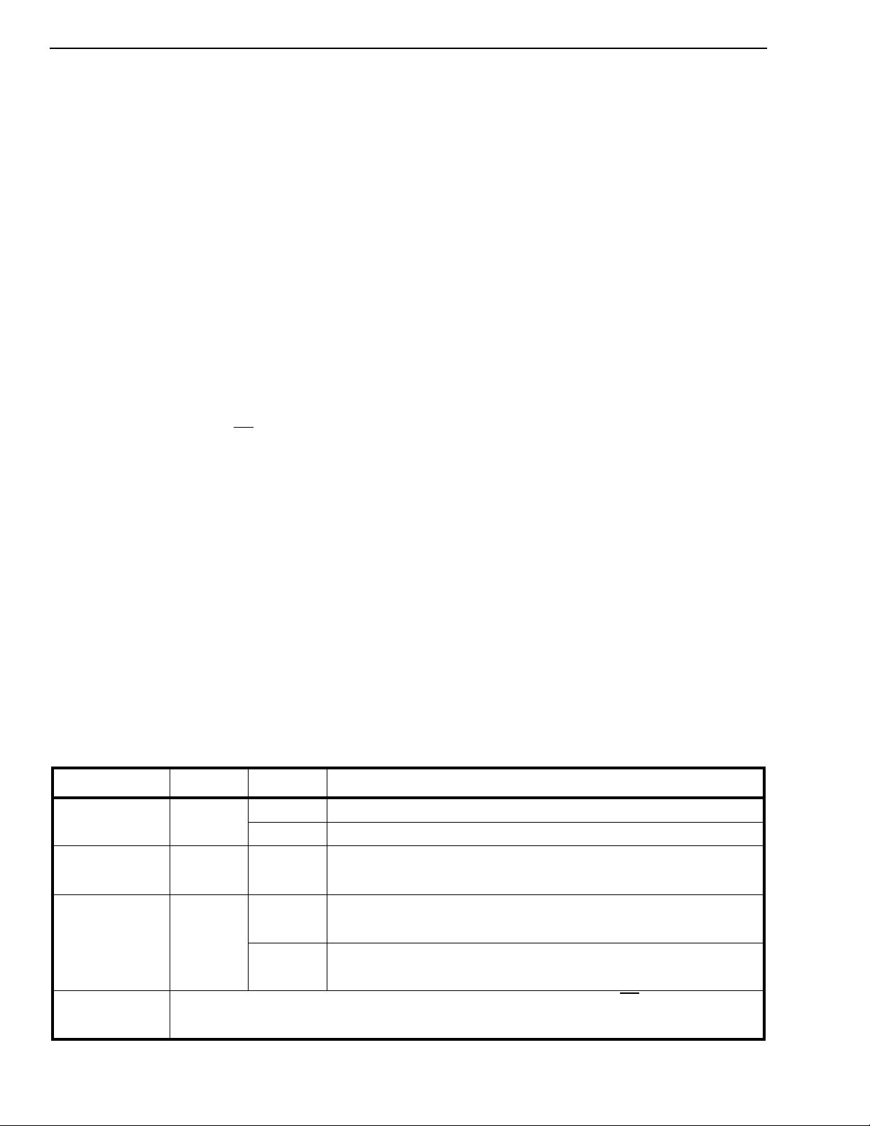
ANUL
V
SD0
SD1
SD2
SD3
SD4
SD5
V
R
X
Transmit
Filter
Output
Register
Receive
Filter
V
Ref
Analog to
Digital PCM
Encoder
A Register
B-Register
PCM Digita l
to Analog
Decoder
GNDA GNDD V
8-Bits
8-Bits
DDVEE
Output
Register
Control
Logic
Input
Register
DSTo
CSTi
CA
F1i
C2i
DSTi
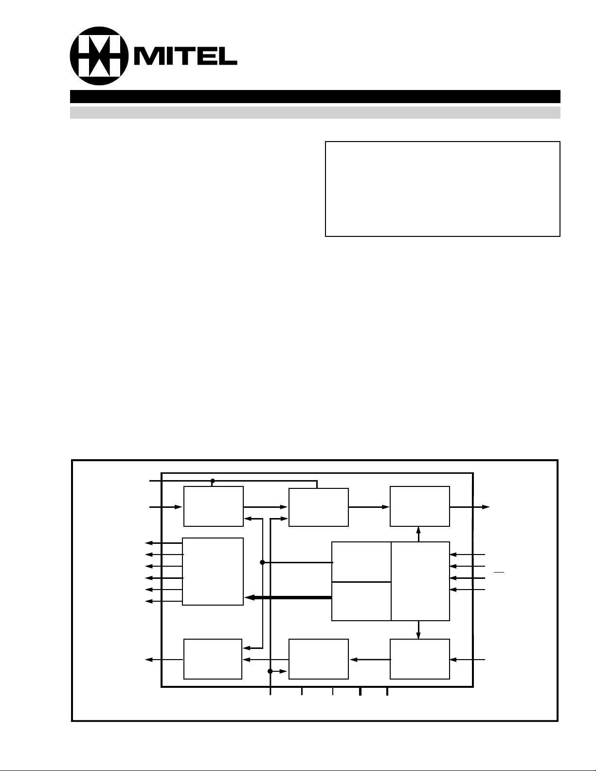
Figure 1 - Functional Block Diagram
6-19
Page 2
MT8960/61/62/63/64/65/66/67 ISO
2
-CMOS
MT8960/61/64/65
CSTi
DSTi
DSTo
VDD
SD3
SD2
1
2
3
C2i
4
5
F1i
6
CA
7
8
9
18 PIN CERDIP/PDIP
18
17
16
15
14
13
12
11
10
GNDD
VRef
GNDA
VR
ANUL
VX
VEE
SD0
SD1
CSTi
DSTi
DSTo
VDD
MT8962/63/66/67
1
2
3
C2i
4
5
SD5
SD4
SD3
6
7
F1i
8
CA
9
10
20 PIN PDIP/SOIC
20
19
18
17
16
15
14
13
12
11
GNDD
VRef
GNDA
VR
ANUL
VX
VEE
SD0
SD1
SD2
Figure 2 - Pin Conne ctions
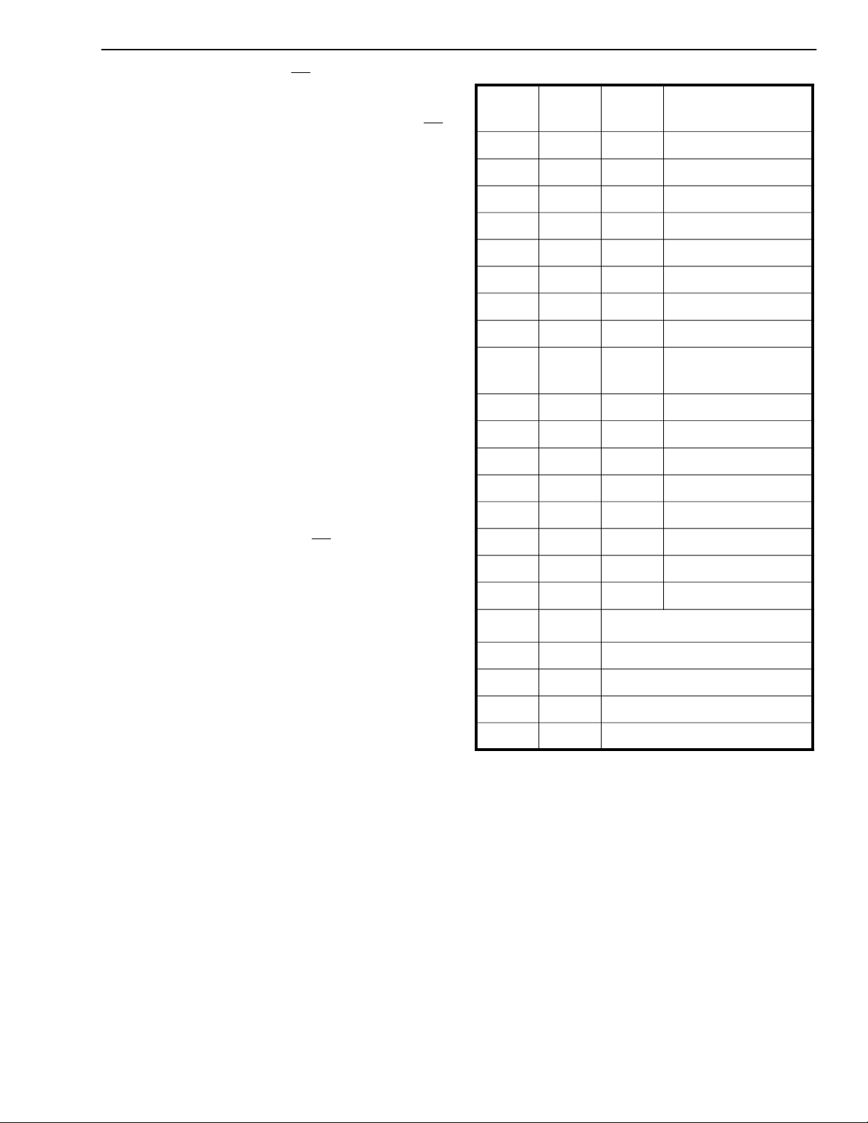
Pin Description
Pin Name Description
CSTi Control ST-BUS In is a TTL-compa tib le digit al inpu t used to control the functi on of the filter/cod ec.
Three modes of operation may be effect ed by applying to this input a logic high (V
(GNDD), or an 8-bit serial word, depending on the logic states of CA and F1i
.
Functions controlled are : powerdown, filter gain adjust, loopba ck, chip testing, SD outputs.
DSTi Data ST-BUS In accepts the incoming 8-bit PCM word. Input is TTL-compatible.
), logic low
DD
C2i Clock Input is a TTL-compatible 2.048 MHz clock.
DSTo Data ST-BUS Out is a three-state digital output driving the PCM bus with the outgoing 8-bit PCM
word.
V
F1i
Positi ve pow er Supp ly (+5V).
DD
Synchronization Input is an active low digital input enabling (in conjunction with CA) the PCM input,
PCM output and digital cont rol input . It is internally sampled on every positive edge of the clock, C2i,
and provides f rame and channel synchronization.
CA Control Address is a three-level digit al input which enabl es PCM input and output and determine s
into which control register (A or B) the serial data, presented to CSTi, is stored.
SD3 System Drive Output is an open drain output of an N-channel transistor which has its source tied to
GNDA. Inactive stat e is open circui t.
SD4-5 System Drive Outputs
are open drain outputs of N-channel transistors which have their source tied
to GNDD. Inactive state is open circuit.
SD0-2 System Drive Outputs
are “Totempole“ CMOS output s switching between GNDD and V
. Inactive
DD
state is logic low.
V
V
ANUL Auto Nul l
Negative power supply (-5V).
EE
Voice Transmit is the analog input to the transmit filter.
X
is used to integrate an internal auto-null signal. A 0.1µF capacitor must be connected
between this pin and GNDA.
V
Voice Receive is the analog output of the receive filter.
R
GNDA Analog ground (0V).
V
Vo ltag e Reference input to D to A converter.
Ref
GNDD Digital grou nd (0V ).
6-20
Page 3
ISO
2
-CMOS MT8960/61/62/63/64/65/66/67
MT8960/62
Digital Ou tput
11111111
11110000
11100000
11010000
11000000
10110000
10100000
10010000
10000000
00000000
00010000
00100000
00110000
01000000
01010000
01100000
01110000
01111111
Bit 7... 0
MSB LSB
-2.415V -1.207V 0V +1.207V +2.415V
Analog Input Voltage (V
)
IN
MT8964/66
Digital Output
10000000
10001111
10011111
10101111
10111111
11001111
11011111
11101111
11111111
01111111
01101111
01011111
01001111
00111111
00101111
00011111
00001111
00000000
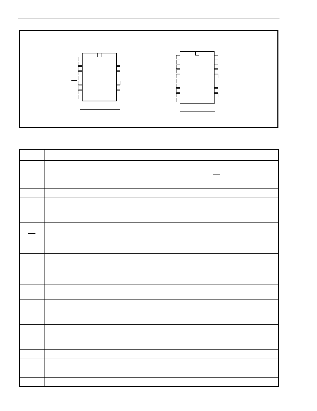
Figure 3 - µ-Law Encoder Transfer Characteristic
MT8961/63
Digital Ou tput
11111111
11110000
11100000
11010000
11000000
10110000
10100000
10010000
10000000
00000000
00010000
00100000
00110000
01000000
01010000
01100000
01110000
01111111
-2.5V -1. 25 V 0V
+1.25V
MT8965/67
Digital Output
+2.5 V
1010 1010
1010 0101
1011 0101
1000 0101
1001 0101
1110 0101
1111 0101
1100 0101
1101 0101
0101 0101
0100 0101
0111 0101
0110 0101
0001 0101
0000 0101
0011 0101
0010 0101
0010 1010
Bit 7... 0
MSB LSB
Analog Input Voltage (V
)
IN
Figure 4 - A-L aw E ncod er Transfer Char ac teristi c
6-21
Page 4

MT8960/61/62/63/64/65/66/67 ISO
2
-CMOS
Functional Description
Figure 1 shows the functional block diagram of the
MT8960-67. These devices provide the conversion
interface between the voiceband analog signals of a
telephone subscriber loop and the digital signals
required in a digital PCM (pulse code modulation)
switching system. Analog (voiceband) signals in the
transmit path enter the chip at V
8kHz, and the samples quantized and assigned 8-bit
digital values defined by logarithmic PCM encoding
laws. Analog signals in the receive path leave the
chip at V
words.
Separate switched capacitor filt er sections are used
for bandlimiting prior to digital encoding in the
transmit path and after digital decoding in the receive
path. All filter clocks are derived f rom the 2.048 MHz
master clock input, C2i. Chip size is minimized by
the use of common circuitry performing the A to D
and D to A conversion. A successive approximation
technique is used with capacitor arrays t o define the
16 steps and 8 chords in the signal conversion
process. Eight-bit PCM encoded digital data enters
and leaves the chip serially on DSTi and DSTo pins,
respectively.
after reconstruction from digital 8-bit
R
, are sampled at
X
are 30 dB for 0-60 Hz and 35 dB for 4.6 kHz and
above.
The filter output signal is an 8 kHz staircase
waveform which is fed into the codec capacitor ar ray,
or alternatively, into an external capacitive load of
250 pF when the c hip is in the test mode. The digital
encoder generates an eight-bit digital word
representation of the 8 kHz sampled analog signal.
The first bit of serial data stream is bit 7 (MSB) and
represents the sign of the analog signal. Bits 4-6
represent the chord which contains the analog
sample value. Bits 0-3 represent the step value of
the analog sample within the selected chord. The
MT8960-63 provide a sign plus magnitude PCM
output code format. The MT8964/66 PCM output
code conforms to the AT &T D3 specification, i.e.,
true sign bit and inverted magnitude bits. The
MT8965/67 PCM output code conforms to the CCITT
specifications with alternate digit inversion (even bits
inverted). See Figs. 3 and 4 for the digital output
code corresponding to the analog voltage, V
input.
The eight-bit digital word is output at DSTo at a
nominal rate of 2.048 MHz, via the output buffer as
the first 8-bit s of the 125 µs sampling frame.
IN
, at V
X
Tra n smit Path
Analog signals at the input (Vx) are firstly
bandlimited to 508 kHz by an RC lowpass filter
section. This performs the necessary anti-aliasing
for the following first-order sampled data lowpass
pre-filter which is clocked at 512 kHz. This further
bandlimits the signal to 124 kHz before a fifth-order
elliptic lowpass filter, clocked at 128 kHz, provides
the 3.4 kHz bandwidth required by the encoder
section. A 50/60 Hz third-order highpass notch filter
clocked at 8 kHz completes the transmit filter pat h.
Accumulated DC offset is cancelled in this last
section by a switched-capacitor auto-zero loop which
integrates the sign bit of th e encoded PCM word, fed
back from the codec and injects this voltage level
into the non-inverting input of the comparator. An
integrating capacitor (of value between 0.1 and 1 µF)
must be externally connected from this point (ANUL)
to the Analog Ground (GNDA).
The absolute gain of the transmit filter (nominally 0
dB at 1 kHz) can be adjusted from 0 dB to 7 dB in 1
dB steps by means of three binary controlled gain
pads.
Receive P ath
An eight-bit PCM encoded digital word is received on
DSTi input once during the 125 µs period and is
loaded into the input register. A charge proportional
to the received PCM word appears on the capacitor
array and an 8 kHz sample and hold circuit
integrates this charge and holds it for the rest of the
sampling period.
The receive (D/A) filter provides interpolation filtering
on the 8 kHz sample and hold signal from the codec.
The filter consists of a 3.4 kHz lowpass fifth-order
elliptic section clocked at 128 kHz and performs
bandlimiting and sm oothing of the 8 kHz "staircase"
waveform. In addition, sinx/x gain correction is
applied to the signal to compensate for the
attenuation of higher frequencies caused by the
capacitive sample and hold circuit. The absolute
gain of the receive f ilter can be adjusted from 0 dB to
-7 dB in 1 dB steps by means of three binary
controlled gain pads. The resulting lowpass
characteristics, with the limits shown in Figure 11,
meet the CCITT and AT & T recommended
specifications.
The resulting bandpass characteristics with the limits
shown in Figure 10 meet the CCITT and AT&T
recommended specifications. Typical atttenuations
6-22
Typical attenuation at 4.6 kHz and above is 30 dB.
The filter is followed by a buffer amplifier which
will drive 5V peak/peak into a 10k ohm load, suitable
for driving electronic 2-4 wire circuits.
Page 5
ISO
2
-CMOS MT8960/61/62/63/64/65/66/67
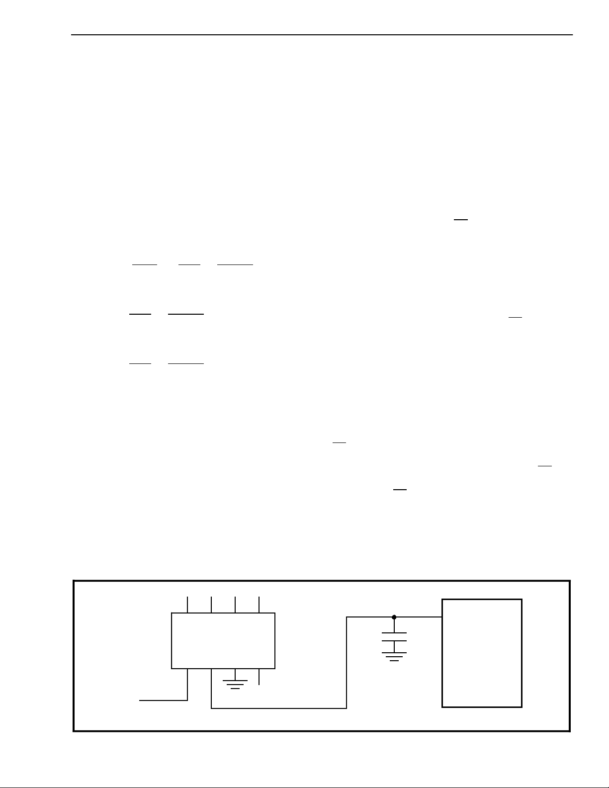
V
Ref
An external voltage must be supplied to the V
Ref
pin
which provides the reference voltage for the digital
encoding and decoding of the analog signal. For
V
= 2.5V, the digital encode decision value for
Ref
overload (maximum analog signal detect level) is
equal to an analog input V
= 2.415V (µ-Law
IN
version) or 2.5V (A-Law version) and is equivalent to
a signal level of 3.17 dBm0 or 3.14 dBm0
respectively, at the cod ec .
The analog output voltage from the decoder at V
is
R
defined as:
µ-Law:
C
V
Ref
X
-0.5 2
[( 128 )+( 128 )( 33 )]
16.5 + S
V
±
OFFSET
A-Law:
2
V
X
Ref
V
X
Ref
C+1
0.5 + S
[( 128 )( 32 )]
C
2
16.5 + S
[( 128 )( 32 )]
V
±
V
±
OFFSET
OFFSET
C=0
C≠0
driving a large number of codecs due to the high
input impedance of the V
input. Normal
Ref
precautions should be taken in PCB layout design to
minimize noise coupling to this pin. A 0.1 µF
capacitor connected from V
to ground and located
Ref
as close as possible to the codec is recommended to
minimize noise entering through V
. This capacitor
Ref
should have good high frequency characteristics.
Timing
The codec operates in a synchronous manner (see
Figure 9a). The codec is activated on the first
positive
digital output at DSTo (which is a three-state output
driver) will then change from a high impedance state
to the sign bit of the encoded PCM word to be
output. This will remain valid until the next positive
edge, when the next most significant bit will be
output.
On the first negative clock edge (after F1i signal has
been internally synchronized and CA is at GNDD or
V
into the input shift register as the sign bit of the
incoming PCM word.
edge of C2i af ter F1i has gone low. The
) the logic signal present at DSTi will be clocked
EE
where C = chord number (0-7)
S = step number (0-15)
is a high impedance input with a varying
V
Ref
capacitive load of up to 40 pF.
The recommended reference volt age for the MT8960
series of codecs is 2.5V ±0.5%. The output voltage
from the reference source should have a maximum
temperature coefficient of 100 ppm/C°. This voltage
should have a total regulation tolerance of ±0.5%
both for changes in the input voltage and output
loading of the voltage reference source. A voltage
reference circuit capable of meeting these
specifications is shown in Figure 5. Analog Devices
’AD1403A voltage reference circuit is capable of
NC
NC NC NC
5678
AD1403A
1234
The eight-bit word is thus input at DSTi on negative
edges of C2i and output at DSTo on positive edges
of C2i.
F1i
must ret urn to a high level after the eighth
clock pulse causing DSTo to enter high impedance
preven ti ng fur th e r input da ta to DS Ti. F1i will
and
continue to be sampled on every positive edge of
C2i. (Note: F1i
may subsequently be taken low
during the same sampling frame to enable entry of
serial data into CSTi. This occurs usually mid-frame,
in conjunction with CA=V
, in order to enter an 8-bit
DD
control word into Re g iste r B. In this case , PC M i n p ut
and output are inhibited by CA at V
V
Ref
0.1 µF
MT8960-67
FILTER/CODEC
DD
.)
+5V
NC
2.5V
Figure 5 - Typical Voltage Reference Circ uit
6-23
Page 6
MT8960/61/62/63/64/65/66/67 ISO
2
-CMOS
Internally the codec will then perform a decode cycle
on the newly input PCM word. The sampled and
held analog signal thus decoded will be updated 25
µs from the start of the c ycle. After this the analog
input from the filter is sample d for 18 µs, after wh ich
digital conversion takes place during the remaining
82 µs of the sampling cycle.
Since a single clock frequency of 2.048 MHz is
required, all digital data is input and output at this
rate. DSTo, therefore, assumes a high impedance
state for all but 3.9 µs of the 125 µs frame. Similarly,
DSTi input data is valid for only 3.9 µs.
Digital Control Functions
CSTi is a digital input (levels GNDD to VDD) which is
used to control the function of the filter/codec. It
operates in three different modes depending on the
logic levels applied to the Control Address input
(CA) and chip enable input (F1i
) (see Table 1).
Mode 1
CA= -5 V (VEE); CSTi=0V (GNDD)
Mode 2
CA= -5V (VEE); CSTi receives an eight-bit control
word
CSTi accepts a serial data stream synchronously
with DSTi (i.e ., it accept s an eight-b it serial wo rd in a
3.9 µs timeslot, updated every 125 µs, and is
specified identically to DSTi for timing
considerations). This eight-bit control word is
entered into Control Register A and enables
programming of the following functions: transmit and
receive gain, powerdown, loopback. Register B is
reset to zero and the SD outputs assume their
inactive state. Test modes cannot be entered.
Mode 3
CA=0V (GNDD); CSTi receives an eight-bit control
word
As in Mode 2, the control word enters Register A and
the aforementioned functions are controlled. In this
mode, however, Register B is not reset, thus not
affecting the states of the SD outputs.
The filter/codec is in normal operation with nominal
transmit and receive gain of 0dB. The SD outputs
are in their active states and the test modes cannot
be entered.
CA = -5V (V
A state of powerdown is forced upon the chip
whereby DSTo becomes high impedance, VR is
connected to GNDA and all analog sections have
power r em o ve d.
MODE CA CSTi FUNCTION
(Note 1)
(Note 2)
); CSTi = +5V (VDD)
EE
1
2V
3
V
EE
EE
GNDD Serial Eight-bit control word int o registe r A. Register B is unaffected.
V
DD
GNDD Norm al chip operation.
V
Serial Eight-bit control word into Register A. Register B is reset.
Data
Data
Serial Eight -bit control word int o registe r A. Register B is unaffected.
Data
DD
Powerdown.
CA=+5V (V
In this case the control word is transferred into
Register B. Register A is unaffected. The input and
output of PCM data is inhibited.
The contents of Register B controls the six
uncommitted outputs SD0-SD5 (four outputs, SD0SD3, on MT8960/61/64/65 versions of chip) and also
provide entry into one of the three test modes of the
chip.
); CSTi receives an 8-bit control word
DD
Note 1: When operating in Mode 1, there should be only one frame pulse (F1i
Note 2: When operating in Mode 3, PCM input and output is inhibited by CA=V
Table 1. Digi ta l Con tr ol M o des
6-24
) per 125 µ s fra me
.
DD
Page 7
2
ISO
-CMOS MT8960/61/62/63/64/65/66/67
Note: For Modes 1 and 2, F1i must be at logic low
for one period of 3.9 µs, in each 125 µs cycle, when
PCM data is being input and output, and the control
word at CSTi enters Register A. For Mode 3, F1i
must be at a logic low f or two periods of 3.9 µs, in
each 125 µs cycle. In the first period, CA must be at
GNDD or V
high (V
, and in the second period CA must be
EE
.
DD)
Control Registers A, B
BIT 2 BIT 1 BIT 0
FILTER GAIN (dB)
000 0
001 + 1
010 + 2
011 + 3
100 + 4
TRANSMIT (A/D)
The contents of these registers control the filter/
codec functions as described in Tables 2 and 3.
Bit 7 of the registers is the M SB and is defined as the
first bit of the serial data stream input (corresponding
to the sign bit of the PCM word).
On initial power-up these registers are set to the
powerdown condition for a maximum of 25 clock
cycles. During this time it is impossible to change
the data in these registers.
Chip Testing
By enabling Register B with valid data (eight-bit
control wor d in put to CSTi when F1i
) the chip testing mode can be entered. Bits 6
V
CC
=GNDD and CA=
and 7 (most sign bits) define states for testing the
transmit filter, receive filter and the codec function.
The input in each case is V
each case is V
output. (See Table 3 for details.)
R
input and the output in
X
Loopback
101 + 5
110 + 6
111 + 7
RECEIVE (D/A)
BIT 5 BIT 4 BIT 3
FILTER GAIN (dB)
000 0
001 - 1
010 - 2
011 - 3
100 - 4
101 - 5
110 - 6
111 - 7
BIT 7 BIT 6 FUNCTION CONTRO L
0 0 Normal operation
0 1 Digital Loopback
Loopback of the filter/codec is controlled by the
control word entered into Register A. Bits 6 and 7
(most sign bits) provide either a digital or analog
loopback condition. Digital loopback is defined as
follows:
• PCM input da ta at DS Ti is latche d in to the P CM
input regis ter an d the out put of this regis ter is
connected to the input of the 3-state PCM
output regist er.
• The digital input to the PCM digital-to-analog
decoder is d isco nnect ed, for ced to ze ro (0).
• The outpu t of the PCM encoder is di sabled and
thus the encoded data is lost . The PCM output
at DSTo is determined by the PCM input data.
Analog loopback is defined as follows:
• PCM input data is latched, decoded and filtered
as normal but not outp ut at V
.
R
1 0 Analog Loopback
1 1 Powerdown
Table 2. Con trol S tates - R eg ister A
• Analog o ut put buffer at V
has its input sh orted
R
to GNDA an d discon nec ted from the rec eive
filter output.
• Analog inp ut at V
is disconnec ted f rom the
X
transmit filter input.
• The receive filter output is connected to the
transmit fi lter inp ut. Th us the deco de sign al is
fed back th rough the rec ei ve path and en c od ed
in the normal way. The analog outp ut bu ffer at
is not tested by this configuration.
V
R
In both cases of loopback, DSTi
is the input
and DSTo is the output.
6-25
Page 8

MT8960/61/62/63/64/65/66/67 ISO
Logic Control Outputs SD0-5
These outputs are directly controlled by the logic
states of bits 0-5 in Register B. A logic low (GNDD)
in Register B causes the SD outputs to assume an
inactive state. A logic high (V
causes the SD outputs to assume an active state
(see Table 3). S D0-2
switch between GNDD and V
and may be used to control external logic or
transistor circuitry, for example, that employed on the
line card for performing such functions as relay drive
for application of ringing to line, message waiting
indication, etc.
SD3-5
are used primarily to drive external analog
circuitry. Examples may include the switching in or
out of gain sections or filter sections (eg., ring trip
filter) (Figure 7).
MT8962/63/66/67 provides all six SD outputs.
) in Register B
DD
DD
2
-CMOS
2 Wire
Analog
Supervision
Protection
Battery
Feed
Ringing
2W/4W
Converter
Telephone Set
PCM Highway
MT8960/61
MT8962/63
MT8964/65
MT8966/67
MT8960/61/64/65 each packaged in an 18-pin DIP
provide only four control output s, SD0-3.
Figure 6 - Typical Line Termination
BITS 0-2 LOGIC CONTROL OUTPUT S SD
0 Inact ive stat e - logic low (GNDD).
1 Act ive st ate - logic high (V
DD
).
BIT 3 LOGIC CONTROL OUTPUT SD
0 Inact ive stat e - High Impedance.
1 Act ive st ate - GNDA.
BITS 4,5 LOGIC CONTROL OUTPUTS SD
0 Inact ive stat e - High Impedance.
1 Active state - GNDD.
BIT 7 BIT 6 CHIP TESTING CONTRO LS
0 0 Normal operation.
0 1 Transmit filter testing, i.e.:
Transmit filter input connected to V
Receive filter and Buffer disconnected from V
input
X
R
1 0 Receive filter testing, i.e.:
Receive filter input connected to V
input
X
Receive filter input disconnected from codec
-SD
0
, SD
4
2
3
5
1 1 Codec testing i.e.:
Codec analog input connected to V
Codec analog input disconnected from transmit filter out put
Codec analog output connected to V
VR disconnected from rece ive f ilter outp ut
6-26
X
R
Table 3. Con trol S tates - Re gis ter B
Page 9

ISO
2
-CMOS MT8960/61/62/63/64/65/66/67
Powerdown
Powerdown of the chip is achieved in several ways:
Internal Con trol:
1) Initial Power-up. Initial application of V
V
causes powerdown for a period of 25 clock
EE
cycles and during this period the chip will
accept input only from C2i. The B-register is
reset to zero forcing SD 0 -5 to be inactive. Bits
0-5 of Register A (gain adjust bits) are forced
to zero and bits 6 and 7 of Register A become
logic high thus reinforcing the powerdown.
2) Loss of C2i. Powerdown is entered 10 to 40
µs after C2i has assumed a continuous logic
high (V
). In this condition the chip will be in
DD
the sam e state as in (1) above.
Note: If C2i stops at a continuous logic low
(GNDD), the digital data and status is
indeterminate.
DD
and
External Contro l:
1) Register A. Powerdown is controlled by bits 6
and 7 ( when both at logic high) of Register A
which in turn receives its co ntrol word input
via CSTi, when F1i
either at V
or GNDD. Power is removed
EE
is low and CA input is
from the filters and analog sections of the chip.
The analog ouput buffer at V
will be
R
connected to GNDA. DSTo becomes high
impedance and the clocks to the majority of the
logic are stopped. SD output s are unaff ected
and may be updated as normal.
2) CSTi
Input. W ith CA at VEE and CSTi held at
continuous logic high the chip assumes the
same state as described in External Control
(1) above.
From ST-BUS
From ST-BUS
Master Clock
to ST-BUS
5V
Alignment
Register Select
MT8960/61/64/65
CSTi
DSTi
C2i
DSTo
V
DD
F1i
CA
SD3
SD2
GNDD
V
Ref
GNDA
V
ANUL
V
V
EE
SD0
SD1
2.5V
R
X
-5V
0.1µF
Ring Trip
Filter
(With Relay
Drive)
Gain
Section
2/4 Wire
Converter
Figure 7 - Typical Use of the Special Drive Outputs
Message
Waiting
(With Relay
Drive)
Ring Feed
(With Relay
Drive)
-100V D C
Telephone
Line
-48V DC
-48V DC
90V
RMS
6-27
Page 10

MT8960/61/62/63/64/65/66/67 ISO
2
-CMOS
Controlling
Micro-
Processor
Speech
Switch
-
8980
DSTi
DSTo
CDTi
V
V
SD0
SDn
X
R
.
•
.
•
.
•
Line
Interface
&
Monitoring
Circuitry
Line 1
MT8960-67
8
8
Repeated for Lines
8
•
•
•
Repeated for Lines
2 to 255
•
•
•
2 to 255
8
Control &
Signalling
-
8980
DSTi
DSTo
CDTi
V
V
SD0
SDn
X
R
.
•
.
•
.
•
Line
Interface
&
Monitoring
Circuitry
Line 256
MT8960-67
Figure 8 - Example Architecture of a Simple Digital Switching System Using the MT8960-67
6-28
Page 11

Absolute Maximum Ratings*
Parameter Symbol Min Max Units
ISO
2
-CMOS MT8960/61/62/63/64/65/66/67
1 DC Supply Voltages V
2 Reference Voltage V
3 Analog Input V
4 Digital Inputs Except CA GNDD-0.3 V
5 Output Voltage SD
6 Current On Any Pin I
7 Storage Temperat u re T
8 Power Dissipation at 25°C
* Exceeding these values may cause permanen t dama ge. Functi onal operati on und er these cond ition s is not implied.
(Derate 16 mW/°C above 75°C) P
-GNDD -0 .3 +6.0 V
DD
-GNDD -6.0 +0.3 V
V
EE
Ref
X
CA V
0-2 G NDD-0.3 V
3 V
SD
4-5 V
SD
I
S
Diss
GNDA V
V
EE
-0.3 VDD+0.3 V
EE
-0.3 VDD+0.3 V
EE
-0.3 VDD+0.3 V
EE
V
DD
DD
20 mA
-55 +125 °C
500 mW
Recommended Operating Conditions - Voltages are with respect to GNDD unless otherwise stated
Characteristics Sym Min Typ* Max Units Comments
1 Supply Voltage V
2 Voltage On Digital Ground
VGNDD
DD
V
EE
V
Ref
4.75 5.0 5.25 V
-5.25 -5.0 -4.75 V
2.5 V See Note 1
-0.1 0.0 +0.1 Vdc Ref. to GNDA
-0.4 0.0 +0.4 Vac Ref. to GNDA 400ns max.
duration in 125µs cycle
3 Operating Temperat u re T
4 Operating Current V
5 Standby Current V
Note 1: Temperature coefficient of V
DD
V
EE
V
Ref
DD
V
EE
should be better than 100 ppm/°C.
Ref
I
DD
I
EE
I
Ref
I
DDO
I
EEO
O
0+70°C
3.0
3.0
4.0
4.0
mAmAAll digital inputs at V
or GNDD (or VEE for CA)
2.0 µA Mean current
0.25
0.25
1.0
1.0
mAmAAll digital inputs at V
or GNDD (or VEE for CA)
DC Electrical Characteristics - Voltages are with respect to GNDD unless otherwise stated.
=0 to 70°C, VDD=5V±5%, VEE=-5V±5 %, V
T
A
otherwise specified.
=2.5V±0.5%, GNDA=GNDD=0V,Clock Frequency =2.048MHz. Outputs unloaded unless
Ref
DD
DD
+0.3 V
+0.3 V
DD
DD
V
V
Characteristics Sym Mi n Typ* Max Units Test Condition s
1
2 Input Low Except CA V
3 Inpu t High Voltage All Inputs V
4 Inpu t Intermediat e CA
5 Output Leakage DSTo
* Typ ical figu res are at 25°C with nomina l ±5V suppl ies. For design aid only: not guaranteed and no t subject to productio n test ing.
Input Current Except CA I
CA I
D
I
G
Voltage CA V
I
T
A
Voltage
L
Current (Tristate) SD
3-5
I
IC
0.0 0.8 V
IL
IIC
V
EE
2.4 5.0 V
IH
0.0 0.8 V
±0.1
ILC
V
I
0Z
10.0 µAVIN = GNDD to V
10.0 µAVIN = VEE to V
VEE+1.2
10.0
V
µA
µA
Output High Impedance
DD
DD
6-29
Page 12

MT8960/61/62/63/64/65/66/67 ISO
DC Electrical Characteristics (con t’d)
Characteristics Sym M in Typ* Max Units Test Con dition s
2
-CMOS
6
7 Ou tput High DSTo V
8 Ou tpu t Resistance SD
9 Ou tput Capacitance DSTo C
10
11 Input Resistance V
12 Input Capacitance V
13 Input Offset Voltage V
14 Ou tput Resistan ce V
15 Ou tpu t Offset Voltage V
Note 2: V
Output Low DSTo V
D
Voltage SD
I
0-2 V
G
I
Voltage SD
T
A
0-2 V
3-5 R
L
Input Current V
A
N
A
L
O
G
specifies the DC c om po ne nt of the di git ally enc od ed PC M wo r d.
OSIN
X
X
X
X
R
R
OL
OL
OH
OH
OUT
OUT
I
IN
R
IN
CIN 30.0 pF f
V
OSIN
R
OUT
V
OSOUT
0.4 V I
1.0 V I
4.0 V I
4.0 V I
1.0 2.0 KΩ V
4.0 pF Output High Impedance
10.0 µAVEE ≤ VIN ≤ V
10.0 MΩ
+1.0 mV See Note 2
100 Ω
100 mV Digital Input= +0
AC Electrical Characteristics - Voltages are with respect to GNDD unless otherwise stated.
=0 to 70°C, VDD=5V±5%, VEE=-5V±5%, V
T
A
otherwise specified.
Characteristics Sym M in Ty p* M ax Units Test Con dition s
1
Clock Frequency C2i f
2 Clock Rise Time C2i t
3 Clock Fall Time C2i t
4 Clock Duty Cycle C2i 40 50 60 %
=2.5V±0.5%, GNDA=GNDD=0V, Clock Frequency=2.048 MHz. Outputs unloaded unless
Ref
2.046 2.048 2.05 MHz See Note 3
C
CR
CF
50 ns
50 ns
=1.6 mA
OUT
=1 mA
OUT
=-100µA
OUT
=-1mA
OUT
=+1V
OUT
= 0 - 4 kHz
IN
CC
5 Chip Enable Rise Time F1i
6 Chip Enable Fall Time F1i
7 Chip Enable Setup Time F1 i
8 Chip Enable Hold Time F1i
D
I
9 Output Rise Time DSTo t
G
10 Output Fall Time DSTo t
I
11 Propagation Delay Clock DSTo
T
to Output Enable
A
12 Propagat ion Dela y DSTo
L
Clock to Output
13 Input Rise Time CSTi
DSTi
14 Input F a ll Time CSTi
DSTi
15 Input S et up Time CS Ti
DSTi
16 Input Hold Time CSTi
DSTi
* Typ ical figu res are at 25°C with nomina l ±5V suppl ies. For design aid only: not guaranteed an d not subject to productio n testing .
t
t
t
t
t
PZL
t
PZH
t
PLH
t
PHL
t
t
t
ISH
t
t
ER
EF
ES
EH
OR
OF
IR
IF
ISL
IH
100 ns
100 ns
50 ns See Note 4
25 ns See Note 4
100 ns
100 ns
122
122
100
100
100
100
100
100
25
0
60
60
ns
ns R
ns
ns
ns
ns
ns
ns
ns
ns
ns
ns
=10KΩ to V
L
CL=100 pF
CC
6-30
Page 13

2
ISO
-CMOS MT8960/61/62/63/64/65/66/67
AC Electrical Characteristics (con t’d)
Characteris tics Sym Min Typ* Max Units Test Conditions
17
18 SD Out put Fall Time SD t
Propagation Delay SD
D
Clock to SD Output
I
G
I
19 SD Output Rise Time SD t
T
A
20 Digital Loopback
L
Time DSTi to DSTo
t
PCS
t
SF
SR
DL
400 ns CL = 100 pF
200 ns CL = 20 pF
400 ns
122 ns
(See Figures 9a, 9b, 9c)
Note 3: The filter characteristics are totally dependent upon the accuracy of the clock frequency providing F1i is s yn c hronized to
Note 4: This gives a 75 ns period, 50 ns before and 25 ns after the 50% point of C2i rising edge, when change in F1i
C2i. The A/D and D/A functions are unaffected by changes in clock frequency.
undetermined state to to the internally synchronized enable signal.
will giv e an
AC Electrical Characteristics - T rans mit (A/D) Path - V o ltages are with respect to GNDD unless otherwise stated.
=0 to 70°C, VDD=5V±5%, VEE=-5V±5%, V
T
A
Filter Gain Setting = 0dB. Outputs unloaded unless otherwise specified.
Characteristics Sym Min Typ* Ma x Units Test Conditions
1
Analog Input at V
equivalent to
X
the overload decision level at
the codec
2 Absolute Gain (0dB setting) G
3 Absolute Gain (+1dB to +7dB
settings)
=2.5V±0.5%, GNDA=GNDD=0V, Clock Frequency = 2.048MHz,
Ref
V
IN
-0.25 +0.25 dB 0 dB m0 @ 1004 Hz
AX
4.829
5.000
V
V
-0.35 +0.35 dB from nominal,
Level at codec:
µ-Law: 3.17 dBm0
PP
A-Law: 3.14 dBm0
PP
See Note 6
@ 1004 Hz
4 Gain Variat ion With Temp G
With Supplies G
A
5 Gain Tracking
N
(See Figure 12) CCITT G712
A
L
(Method 1)
O
G
CCITT G712
(Method 2)
AT&T
GT
GT
AXT
AXS
X1
-0.25
-0.25
-0.50
X2
-0.25
-0.50
-1.50
6 Quantization
Distortion
(See Figure 13) CCITT G712
(Method 1)
D
QX1
28.00
35.60
33.90
29.30
14.20
* Typical figu res are at 25°C with nomina l ±5V suppl ies. For design aid only: not guaranteed an d not subject to productio n testing.
0.01 dB TA=0°C to 70°C
0.04 dB/V
Sinusoidal Level:
+0.25
dB
+3 to -20 dBm0
Noise Signal Level:
+0.25
+0.50
dB
dB
-10 to -55 dBm0
-55 to -60 dBm0
Sinusoidal Level:
+0.25
+0.50
+1.50
dB
dB
dB
+3 to -40 dBm0
-40 to -50 dBm0
-50 to -55 dBm0
Noise Signal Level:
dB
dB
dB
dB
dB
-3 dBm0
-6 to -27 dBm0
-34 dBm0
-40 dBm0
-55 dBm0
6-31
Page 14

MT8960/61/62/63/64/65/66/67 ISO
T ra nsmit (A/D) Path (cont’d )
Characteristics Sym Min Typ* Max Units Test Conditions
2
-CMOS
Quantization CCITT G712
D
Distortion (Method 2)
(cont’d) AT&T
(See Figure 13)
7 Idle Channel C-mes sage N
Noise Psophometric N
8 Single Frequency Noise N
9 Harm onic Distort ion
(2nd or 3rd Harmonic)
10 Envelope Del ay D
11 Envelope Delay 100 0-2600 Hz
Variation With 600-3000 Hz
Frequency 400-3200 Hz
12 Intermodulation CCITT G712
Distortion 50/60 Hz
A
IMD
N
A
L
CCITT G712
2 tone
IMD
O
G
AT&T IMD
4 tone IMD
13 Gain Relative to ≤50 Hz
Gain @ 1004 Hz 60 H z
(See Figure 10) 200 Hz
300-3000 Hz
3200 Hz
3300 Hz
3400 Hz
4000 Hz
≥4600 Hz
D
G
QX2
CX
PX
SFX
AX
DX
RX
X1
X2
X3
X4
35.30
29.30
24.30
-1.8
-0.125
-0.275
-0.350
-0.80
60
150
250
Sinusoidal Input Level:
dB
dB
dB
0 to -30 dBm0
-40 dBm0
-45 dBm0
18 dBrnC0 µ-Law Onl y
-67 dBm0p CCITT G712
-56 dBm0 CCITT G712
-46 dB Input Signal:
0 dBm0 @ 1.02 kHz
270 µs @ 1004 Hz
µs
Input Signal:
µs
400-3200 Hz Sinewave
µs
at 0 dBm0
-55 dB 50/60 Hz @ -23 dBm0
and any signal within
300-3400 Hz at -9 dBm0
-41 dB 740 Hz and 1255 Hz
@ -4 to -21 dBm0.
Equal Input Levels
-47 dB 2nd order products
-49 dB 3rd order products
-25
-30
0.00
0.125
0.125
0.030
-0.100
-14
-32
dB
dB
dB
dB
dB
dB
dB
dB
dB
0 dBm0 Input Signal
Transmit
Filter
Response
14 Crosstalk D/A to A/D CT
RT
-70 dB 0 dBm0 @ 1.0 2 kHz
in D/A
15 Power Supply V
Rejection V
DD
EE
PSSR
PSSR
33
1
35
2
dBdBInput 50 mV
1.02 kHz
RMS
at
16 Overload Distortion (See Fig.15) Input frequency=1.02kHz
* Typical figu res are at 25°C with nomina l ±5V suppl ies. For design aid only: not guaranteed an d not subject to productio n testing.
Note 6: 0dBm0=1.1 8 5 V
0dBm0= 1.2 3 1 V
6-32
for the µ -Law codec.
RMS
for the A-Law codec.
RMS
Page 15

2
ISO
-CMOS MT8960/61/62/63/64/65/66/67
AC Electrical Characteristics - Receive (D/A) Path - Voltages are with respect to GNDD unless otherwise stated.
=0 to 70°C, VDD=5V±5%, VEE=-5V±5%, V
T
A
Filter Gain Setting = 0dB. Outputs unloaded unless otherwise specified.
Characteristi cs Sym M in Typ* M ax Uni ts Test Conditions
=2.5V±0.5%, GNDA=GNDD=0V, Clock Frequency = 2.048MHz,
Ref
1
Analog out put at V
R
V
equivalent to the overload
decision level at codec
2 Absolute Gain (0dB setting) G
3 Absolute Attenuation (-1dB
to -7dB settings)
4 G ain Variation With Temp. G
With Supplies G
5 G ain Tracking CCITT G712
GT
(See Figure 12) (Method 1)
CCITT G712
GT
(Method 2)
A
AT & T
N
A
6 Quantization CCITT G712
L
Distortion (Method 1)
O
(See Fig. 13)
G
D
OUT
AR
ART
ARS
R1
R2
QR1
Level at codec:
4.829
5.000
V
V
µ-Law: 3.17 dBm0
pp
A-Law: 3.14 dB m0
pp
=10 KΩ
R
L
See Note 7
-0.25 +0.25 dB 0 dBm0 @ 1004Hz
-0.35 +0.35 dB From nominal,
@ 1004Hz
0.01 dB TA=0°C to 70°C
0.04 dB/V
Sinusoidal Level:
-0.25
+0.25
dB
+3 to -10 dBm0
Noise Signal Level:
-0.25
-0.50
+0.25
+0.50
dB
dB
-10 to -55 dBm0
-55 to -60 dBm0
Sinusoidal Level:
-0.25
-0.50
-1.50
+0.25
+0.50
+1.50
dB
dB
dB
+3 to -40 dBm0
-40 to -50 dBm0
-50 to -55 dBm0
Noise Signal Level:
28.00
35.60
33.90
29.30
14.30
dB
dB
dB
dB
dB
-3 dBm0
-6 to -27 dBm0
-34 dBm0
-40 dBm0
-55 dBm0
CCITT G712
(Method 2)
AT & T
7 Idle Channel C-message N
Noise Psophometric N
8 Si ngle Frequ ency Noise N
9 Harmonic Distortion
(2nd or 3rd Harmonic)
10 Intermodulation CCITT G712
D
QR2
IMD
CR
PR
SFR
R2
36.40
30.40
25.40
dB
dB
dB
12 dBrnC0 µ-Law Only
-75 dBm0p CCITT G712
-56 dBm0 CCITT G712
-46 d B Input Signa l 0 dBm0
-41 dB
Sinusoidal Input Level:
0 to -30 dBm0
-40 dBm0
-45 dBm0
at 1.02 kHz
Distortion 2 tone
AT & T IMD
4 tone IM D
* Typical figu res are at 25°C with nomina l ±5V suppl ies. For design aid only: not guaranteed an d not subject to productio n testing.
R3
R4
-47 dB 2nd order products
-49 dB 3rd order products
6-33
Page 16

MT8960/61/62/63/64/65/66/67 ISO
AAAA
AAAA
AAAA
AAAA
AAAA
AAAA
AAAA
AAA
A
A
A
AAA
AAAA
AAAA
AAAA
AAAA
AAAA
AAAA
AAAA
AAAA
AAAA
AAAA
AAAA
AAAA
AAAA
AAAA
AAAA
AAAA
AA
AA
AA
AA
AAAA
AAAA
AAAA
AAAA
AAAA
AAAA
AAAA
AAAA
AA
AA
AA
AA
Receive (D/A) Path (cont’d)
Characteristics Sym Min Typ* Max Units Test Conditions
2
-CMOS
11
Envelope Delay D
12 Enve lope Delay 1000-2 600 Hz
Variat ion wit h 600-3000 Hz
Frequency 400-3200 Hz
13 Gain Relative to < 200 Hz
Gain @ 1004 Hz 200 H z
A
(See Figure 11) 300-3000 Hz
N
A
L
O
3300 Hz
3400 Hz
4000 Hz
≥4600 Hz
AR
D
DR
90
170
265
G
RR
-0.5
-0.125
-0.350
-0.80
210 µs @ 1004 Hz
µs
Input Signal:
µs
400 - 3200 Hz digital
µs
sinewave at 0 dBm0
0.125
0.125
0.125
0.030
-0.100
-14.0
-28.0
dB
0 dBm0 Input Signal
dB
dB
Receive
dB
Filte r
dB
Response
dB
dB
G
14 Crosstalk A/D to D/A CT
TR
-70 dB 0 dBm0 @ 1.02 kHz
in A/D
15 Power Supply V
Rejection V
16 Overload Distortion
DD
EE
PSRR
PSRR
33
3
35
4
dBdBInput 50 mV
1.02 kHz
RMS
at
Input frequency=1.02 kHz
(See Fig. 15)
* Typical figu res are at 25°C with nomina l ±5V suppl ies. For design aid only: not guaranteed an d not subject to productio n testing.
Note 7: 0dBm0=1.185 V
for µ-Law codec and 0dBm0=1.231 V
RMS
for A-Law codec.
RMS
125 µs
C2i
INPUT
F1i
INTERNAL
ENABLE
DSTo
OUTPUT
DSTi
INPUT
5V
CA
(Mode 3)
0V
CSTi
INPUT
LOAD
A-REGISTER
AAA
AA
AAA
AA
76543210
AAA
AA
AAA
AA
HIGH IMPEDANCE
76543210
76543210 76543210
7
7
6
76
B-REGISTER
6-34
LOAD
Figure 9a - Timi ng D ia gra m - 125 µs Frame Period
Page 17

2
AAAA
AAAA
AAAA
AAAA
AAAA
AAAA
AAAA
AA
ISO
-CMOS MT8960/61/62/63/64/65/66/67
8 CLOCK CYCLES
(See Note)
C2i
Input
t
EF
90%
50%
10%
t
CR
t
CF
t
ER
90%
F1i
Input
DSTo
Output
10%
t
high
impedance
ES
t
EH
t
ES
t
EH
t
ES
t
EH
high-Z
t
t
PZL
t
PZH
PZL
t
PZH
Figur e 9b - Tim ing Dia gr am - Out pu t En ab le
Note: In ty p ic al ap pl ic at ion s , F1i will remain low for 8 cycles of C2i. However, the device will function normally as long as tES and
t
are met at each positive edge of C2i.
EH
C2i
Input
DSTo
Output
DSTi, CSTi
Input
90%
50%
10%
90%
50%
10%
90%
50%
10%
t
PLH
t
CR
t
IR
t
ISH
t
OR
t
CF
t
PLH
t
t
IH
IF
Figure 9c - Timi ng D iag ra m - I npu t/Ou tp u t
t
OF
t
ISL
6-35
Page 18

MT8960/61/62/63/64/65/66/67 ISO
AA
AA
AA
AA
AA
AA
AA
AA
AA
AA
AA
AA
AA
AA
AAAA
A
A
A
A
AA
AAAA
AAAA
AAAA
AAAA
AAAA
AAAA
AAAA
AAAA
AAAA
AAAA
AAAA
AAAA
AAAA
AAAA
AAAA
AAAA
AAAA
AAAA
AAAA
AAAA
AAAA
AAAA
AAAA
AAAA
AAAA
AAAA
AAAA
AAAA
AAAA
AAAA
AAAA
AAAA
AAAA
AAAA
AAAA
AAAA
AAAA
AAAA
AAAA
AAAA
AAAA
AAAA
AAAA
AAAA
AAAA
AAAA
AAAA
AAAA
AAAA
AAAA
AAA
AAA
AAA
AAA
AAA
AAA
AAA
AAA
AAA
AAA
AAA
AAA
AAA
AAA
AAA
AAA
AAA
AAA
AAA
AAA
AAA
AAA
AAA
AAA
AAA
AAAA
AAAA
AAAA
AAAA
AAAA
AAAA
AAAA
AAAA
AAAA
AAAA
AAAA
AAAA
AAAA
AAAA
AAAA
AAAA
AAAA
AAAA
AAAA
AAAA
AAAA
AAAA
AAAA
AAAA
AAAA
AAAA
AAAA
AAAA
AAAA
AAAA
AAAA
AAAA
AAAA
AAAA
AAAA
AAAA
AAAA
AAAA
AAAA
AAAA
AAAA
AAAA
AAAA
AAAA
AAAA
AAAA
AAAA
AAAA
AAAA
AAAA
A
A
A
A
A
A
A
A
A
A
A
A
A
A
A
A
A
A
A
A
A
A
A
A
A
A
A
AAA
AAAA
AAAA
AAAA
AAAA
AAAA
AAAA
AAAA
AAAA
AAAA
AAAA
AAAA
AAAA
AAAA
AAAA
AAAA
AAAA
AAAA
AAAA
AAAA
AAAA
AAAA
AAAA
AAAA
AAAA
AAAA
AAAA
AAAA
AAAA
AAAA
A
A
AA
AAAA
AAAA
AAAA
AAAA
AAAA
AAAA
AAA
AAA
AAA
AAA
AAA
AAA
A
A
A
A
A
A
A
A
A
A
A
A
A
A
A
A
A
A
A
A
A
A
A
A
A
A
AAAA
AAAA
AAAA
AAAA
AAAA
A
A
A
A
A
AAAA
AAAA
AAAA
AAAA
AAAA
AAAA
AAAA
AAAA
AAAA
AAA
AAA
AAA
AAAA
AAAA
AAAA
AAAA
AAAA
AAAA
AAAA
AAAA
AAAA
AAA
AAA
AAA
A
A
A
A
A
A
AAAA
AAAA
AAAA
AAAA
AAAA
AAAA
AAAA
AAAA
AAAA
AAAA
AAAA
AAAA
AAAA
AAAA
AAAA
AAAA
AAAA
AAAA
AAAA
AAAA
AAAA
AAAA
AAAA
AAAA
AAAA
AAAA
AAAA
AAAA
AAAA
AAAA
AAAA
AAAA
A
A
A
A
A
A
A
A
A
A
A
A
A
A
A
A
AAAA
AAAA
AAAA
AAAA
AAAA
AAAA
AAAA
AAAA
AAAA
AAAA
AAAA
AAAA
AAAA
AAAA
AAAA
AAAA
AAAA
AAAA
AAAA
AAAA
AAAA
AAAA
AAAA
AAAA
AAAA
AAAA
AAAA
AAAA
A
A
A
A
A
A
A
A
A
A
A
A
A
A
A
A
A
A
A
A
A
A
A
A
A
A
A
A
A
A
A
A
A
A
A
A
A
A
A
A
A
A
A
A
A
A
A
A
A
A
A
A
A
A
A
A
A
A
A
A
A
A
A
A
A
A
A
A
A
A
A
A
A
A
A
A
A
A
A
A
A
A
A
A
A
A
A
A
A
A
A
AAAA
A
A
A
A
AAAA
AAAA
AAAA
AAAA
AAAA
AAAA
AAAA
AAAA
AAAA
AAAA
AAA
AAA
AAA
AAA
AAAA
AAAA
AAAA
AAAA
AAAA
AAAA
AAA
AAA
AAA
AAA
AAA
AAA
AAAA
AAAA
AAAA
AAAA
AAAA
AAAA
AAAA
AAAA
AAAA
AAAA
AAAA
AAAA
AAAA
AAAA
AAAA
AAAA
AAAA
AAAA
AAAA
AAAA
AAAA
AAAA
AAAA
AAAA
AAAA
AAAA
AAAA
AAAA
AAAA
AAAA
AAAA
AAAA
AAAA
AAAA
AAAA
AAAA
AAAA
AAAA
AAAA
AAAA
AAAA
AAAA
AAAA
AAAA
AAAA
AAAA
AAAA
AAAA
AAAA
AA
AA
AA
AA
AA
AA
AA
AA
AA
AA
A
A
A
AAA
AAAA
AAAA
AAAA
AAAA
AAAA
AAAA
AAAA
AAAA
AAAA
AAAA
AAAA
AAAA
AAAA
AAAA
AAAA
AAAA
AAAA
AAAA
AAAA
AAAA
AAAA
AAAA
AAAA
AAAA
AAAA
AAAA
AAAA
AAAA
AAAA
AAAA
AAAA
AAAA
A
A
A
AA
AAAA
AAAA
AAAA
AAAA
AAA
AAA
AAA
AAA
A
A
A
A
A
A
A
A
A
A
A
A
A
A
A
A
A
A
A
A
A
A
A
A
A
A
A
A
A
A
A
A
A
A
A
A
A
A
A
A
A
A
A
A
A
A
A
AAAA
AAAA
AAAA
AAAA
AAAA
AAAA
AAAA
AAAA
AAAA
AAAA
AAAA
AAAA
AAAA
AAAA
AAAA
AAAA
AAAA
AAAA
AAAA
AAAA
AAAA
AAAA
AAAA
AAAA
AAAA
A
A
AAA
AAAA
AAAA
AAAA
AAAA
AAAA
AAAA
AAAA
AAAA
AAAA
AAAA
AAAA
AAAA
AAAA
AAAA
AAAA
AAAA
AAAA
AAAA
AAAA
AAAA
AAAA
AAAA
AAAA
AAAA
AAAA
AAAA
AAAA
AAAA
AAAA
AAAA
AAAA
AAAA
AAAA
AAAA
AAAA
AAAA
AAAA
AAAA
AAAA
AAAA
AAAA
AAAA
AAAA
AAAA
AAAA
AAAA
AAAA
AAAA
AAAA
AAAA
AAAA
AAAA
AAAA
AAAA
AAAA
AAAA
AAAA
AAAA
AAAA
AAAA
AAAA
AAAA
AAAA
AAAA
AAAA
AAAA
AAAA
AAAA
AAAA
AAAA
AAAA
AAAA
AAAA
AAAA
AAAA
AAAA
AAAA
AAAA
AAAA
AAAA
AAAA
AAAA
AAAA
AAAA
AAAA
AAAA
AAAA
AAAA
AAAA
AAAA
AAAA
AAAA
AAAA
AAAA
AAAA
AAAA
AAAA
AAAA
AAAA
AAAA
AAAA
AAAA
AAAA
AAAA
AAAA
AAAA
AAAA
AAAA
AAAA
AAAA
AAAA
AAAA
AAAA
AAAA
AAAA
AAAA
AAAA
AAAA
AAAA
AAAA
AAAA
AAAA
AAAA
AAAA
AAAA
AAAA
AAAA
AAAA
AAAA
AAAA
AAAA
AAAA
AAAA
AAAA
AAAA
AAAA
AAAA
AAAA
AAAA
AAAA
AAAA
AAAA
AAAA
AAAA
AAAA
AAAA
AAAA
AAAA
AAAA
AAAA
AAAA
AAAA
AAAA
AAAA
AAAA
AAAA
AAAA
AAAA
AAAA
AAAA
AAAA
AAAA
AAAA
AAAA
AAAA
AAAA
AAAA
AAAA
AAAA
AAAA
AAAA
AAAA
AAAA
AAAA
AAAA
AAAA
AAAA
AAAA
AAAA
AAAA
AAAA
AAAA
AAAA
AAAA
AAAA
AAAA
AAAA
AAAA
AAAA
AAAA
AAAA
AAAA
AAAA
AAAA
AAAA
AAAA
AAAA
AAAA
AAAA
AAAA
AAAA
AAAA
AAAA
AAAA
AAAA
AAAA
AAAA
AAAA
AAAA
AAAA
AAAA
AAAA
AAAA
AAAA
AAAA
AAAA
AAAA
AAAA
AAAA
AAAA
AAAA
AAAA
AAAA
AAAA
AAAA
AAAA
AAAA
AAAA
AAAA
AAAA
AAAA
AAAA
AAAA
AAAA
AAAA
AAAA
AAAA
AAAA
AAAA
AAAA
AAAA
AAAA
AAAA
AAAA
AAAA
AAAA
AAAA
AAAA
AAAA
AAAA
AAAA
AAAA
AAAA
AAAA
AAAA
AAAA
AAAA
AAAA
AAAA
AAAA
AAAA
AAAA
AAAA
AAAA
AAAA
AAAA
AAAA
AAAA
AAAA
AAAA
AAAA
AAAA
AAAA
AAAA
AAAA
AAAA
AAAA
AAAA
AAAA
AAAA
AAAA
AAAA
AAAA
AAAA
AAAA
AAAA
AAAA
AAAA
AAAA
AAAA
AAAA
AAAA
AAAA
AAAA
AAAA
AAAA
AAAA
AAAA
AAAA
AAAA
AAAA
AAAA
AAAA
AAAA
AAAA
AAAA
AAAA
AAAA
AAAA
AAAA
AAAA
AAAA
AAAA
AAAA
AAAA
AAAA
AAAA
AAAA
AAAA
AAAA
AAAA
AAAA
AAAA
AAAA
AAAA
AAAA
AAAA
AAAA
AAAA
AAAA
AAAA
AAAA
AAAA
AAAA
AAAA
AAAA
AAAA
AAAA
AAAA
AAAA
AAAA
AAAA
AAAA
AAAA
AAAA
AA
AA
AA
AA
AA
AA
AA
AA
AA
AA
AA
AA
AA
AA
AA
AA
AA
AA
AA
AA
AA
AA
AA
AA
AA
AA
AA
AA
AA
AA
AA
AA
A
A
A
A
A
A
A
A
A
A
A
A
A
A
A
A
A
A
A
A
A
A
A
A
A
A
A
A
A
A
A
A
A
A
A
A
A
A
A
A
A
A
A
A
AAAA
AAAA
AAAA
AAAA
AAAA
AAAA
AAAA
AAAA
A
A
A
AAAA
AAAA
AAAA
AAAA
AAAA
A
A
A
A
A
AAA
AAAA
AAAA
AAA
AAA
2
-CMOS
SCALE B SCALE A PASSBAND ATTENUATION SCALE BSCALE A
Attenuation
Relative To
Attenuation
At 1 kHz (dB)
0 5060100 200 300 3000 3200 3300 3400 4000 4600 5000 10000
AAA
AAA
A
AAA
A
AAA
A
AA
0
10
20
25
30
40
-0.125
0.35
1
2
3
4
AAA
AAA
AAA
AAA
AAA
AAA
AAA
AAA
AAA
AAA
AAA
AAA
AAA
AAA
AAA
AAA
AAA
AAA
AAA
AAA
AAA
AAA
AAA
AAA
AAA
AAA
AAA
AAA
AAA
AAA
AAA
AAA
AAA
AAA
AAA
AAA
A
A
A
AA
AA
AA
AA
AA
AA
AA
AA
AA
AA
AA
AA
AA
AA
AA
AA
AA
AA
AA
AA
AA
AA
AA
AA
AA
AAA
AAA
AAA
AAA
AAA
AA
AA
AA
AA
AA
AA
-0.125
0.125
0.35
AAA
1
AAA
AAA
AAA
AAA
AAA
AAA
AAA
AAA
AAA
AAA
AAA
2
AAA
AAA
AAA
AAA
AAA
AAA
AAA
AAA
AAA
AAA
3
AAA
AAA
AAA
AAA
AAA
AAA
AAA
AAA
AAA
AAA
AAA
4
AAA
AAA
AAA
AAA
AAA
AAA
AAA
AAA
AAA
AAA
10
14
20
30
32
40
STOPBAND ATTENUATION
∏(4000-F)
SIN
-14
-18
SIN
Note: Above function
crossover occurs
at 4000Hz.
AAA
AAA
AAA
AAA
AAAA
AAAA
AAAA
AAAA
1200
∏(4000-F)
1200
AAA
AAA
AAA
AAA
AAA
AAA
AAA
AAA
AAAA
AAAA
AAAA
AAAA
- 1
-7/9
A
A
A
A
FREQUENCY (Hz)
Attenuation
Relative To
Attenuation
At 1 kHz (dB)
6-36
Figure 10 - Attenuation vs Frequency for Transmit (A/D) Filter
0.35
1
2
3
4
AAA
AAA
AAA
AAA
AAA
AAA
AAA
AAA
AAA
AAA
AAA
AAA
AAA
AAA
AAA
AAA
AAA
AAA
AAA
AAA
AAA
AAA
AAA
AAA
AAA
AAA
AAA
AAA
AAA
AAA
AAA
AAA
AAA
AAA
AAA
AAA
AAA
AAA
AAA
AAA
AAA
AAA
AAA
AAA
SCALE BSCALE A
STOPBAND ATTENUATION
-14
1200
∏(4000-F)
SIN
10
14
20
28
30
40
SCALE A
AAAA
AAAA
AAAA
AAAA
AAAA
AAAA
AAAA
AAAA
AAAA
AAAA
AAAA
AAAA
AAAA
AAAA
AAAA
0
1
2
3
4
0 100 200 300 3000 3200 3300 3400 4000 4600 5000 10000
Figure 11 - Attenuation vs Frequency for Receive (D/A) Filter
PASSBAND ATTENUATION
AAAA
AAAA
AAAA
AAAA
AAAA
AAA
AAA
AAA
AAA
AAA
AAA
AAA
AAA
AAA
AAA
AAA
AAA
AAA
AAA
AAA
AAA
AAA
AAA
AAA
AAA
AAA
AAA
AAA
AAA
AAA
AAA
AAA
AAA
AAA
AAA
AAA
AAA
AAA
AAA
AAA
AAA
AAA
AAA
AAA
AAA
AAA
AAA
AAA
AAA
AAA
AAA
AAA
AAAA
AAAA
AAAA
AAAA
AAAA
AAAA
AAAA
AAA
A
AAA
A
AAA
A
FREQUENCY (Hz)
AAA
AAA
AAA
AAA
AAA
AAA
AA
AA
AA
AA
AA
AA
-0.125
0.125
- 1
Page 19

AAAA
AAAA
AAAA
AAAA
AAAA
AAAA
AAAA
AAAA
AAAA
AAAA
A
A
AAAA
A
A
A
A
A
A
A
A
A
A
A
A
A
A
A
A
A
A
A
A
A
A
A
A
AAAA
AAAA
AAAA
AA
AA
AA
AAAA
AAAA
AAAA
AAAA
AAAA
AAAA
AAAA
AAAA
AAAA
AAAA
A
A
AAAA
A
A
A
A
A
A
A
A
A
A
A
A
A
A
A
AAAA
AAAA
AAAA
AA
AA
AA
A
A
A
A
A
A
A
A
A
A
A
A
A
A
A
A
A
A
A
A
A
A
A
A
A
A
A
A
A
A
A
A
A
A
A
A
A
A
A
A
AAAA
AAAA
A
A
AAA
AAAA
AAAA
A
A
AAA
A
A
A
A
A
A
A
A
A
A
A
A
A
AAAA
AAAA
A
A
AAA
A
A
A
AAAA
AAAA
A
A
AAA
A
A
A
A
A
A
A
A
A
A
+0.25
-0.25
Gain Variation (dB)
5a. CCITT Method 1
+1.0
+0.5
0
-0.5
-1.0
Bandlimited White Noise Te st Signal
2
AAA
AAA
AAA
AAA
AAA
AAA
AAA
AAA
AAA
AAA
AAA
AAA
AAA
AAA
AAA
AAA
AAA
CCITT End-To-End Spec
AAAA
AAAA
AAAA
AAAA
AAAA
AAAA
AAAA
AAAA
AAAA
AAAA
AAAA
AAAA
ISO
AAAA
AAAA
AAAA
-CMOS MT8960/61/62/63/64/65/66/67
AA
AA
AA
AA
AA
AA
AA
AA
AA
AA
AA
AAAA
AAAA
AAAA
AAAA
AAAA
AAAA
AAAA
AAAA
AAAA
AAAA
AAAA
AAAA
AAAA
AAAA
AAAA
AAA
AAA
AAA
AA
AA
AA
AA
-60 -55 -50 -40 -30 -20 -10
AAA
AAAA
AAAA
AAAA
AAAA
AAAA
AAAA
AAAA
AAAA
AAAA
AAAA
AAA
AAAA
AAAA
AAA
AAA
AA
AA
AA
AA
AA
AA
AA
AA
AA
AA
AA
AA
AA
AA
AA
AAA
AAA
AAA
AAA
AAA
AAA
AAA
AAA
AAA
AAA
AAA
AAA
AAA
AAA
AAA
AAA
AAA
AAAA
AAAA
AAAA
AAAA
AAAA
AAAA
AAAA
AAAA
AAAA
AAAA
AAAA
AAAA
AAAA
AAAA
AAAA
AAAA
AAAA
AAAA
+1.0
+0.5
+0.25
-0.25
-0.5
-1.0
AAA
AAAA
AAA
AAAA
AAA
AAAA
0
-10 0 -3
AAA
AAAA
AAA
AAAA
AAA
AAAA
Sinusiodal Test Signal
AAAA
AAAA
AAAA
AAAA
AAAA
AAAA
AAA
AAA
AAA
AAA
AAA
AAA
AAA
AAA
AAA
AAA
AAA
AAA
AAA
AAA
AAA
AAA
AAA
AAA
AAA
AAA
AAA
AAA
AAA
AAA
AAA
AAA
AAA
AAA
AAA
AAA
AA
AA
AA
AA
AA
AA
1
Channel Spec
2
Input Le ve l
(dBm0)
5b. CCITT Method 2
AAAA
AAAA
AAAA
AAAA
AAAA
AAAA
AAAA
AAAA
AAAA
AAAA
AAAA
AAAA
AAA
AAA
AAA
AAA
AAA
AAA
AAA
AAA
AAA
AAA
AAA
AAA
AAA
AAA
AAA
AAA
AAA
AAA
AAA
AAA
AAA
AAA
AAA
AAA
AAA
AAA
AAA
AAA
AAA
AAA
AAA
AAA
AAA
AAA
AAA
AAA
AAA
AAA
AAA
AAA
AAA
AAA
AAA
AAA
AAA
AAA
AAA
AAA
AAA
AAA
AAA
A
A
A
A
A
A
1
Channel Spec
2
Input Level
(dBm0)
AAA
AAA
AAA
AAA
+1.5
+1.0
+0.5
AAA
AAA
AAA
AAA
AAA
AAA
AAA
AAA
AAA
AAA
AAA
AAA
AAA
AAA
AAAA
AAAA
AAAA
AAAA
AAAA
AAAA
AA
AA
AA
CCITT End -To -En d Spe c
AAA
AAA
AAA
AAA
AAA
AAA
AAA
AAAA
AAAA
AAAA
AAA
AAAA
AAA
AAAA
AAA
AAAA
AAAA
AAAA
AAAA
AAAA
AAAA
AAAA
AAAA
AAAA
AAAA
AAAA
AAAA
AAAA
AAAA
AAAA
AAAA
AAAA
AAAA
AAAA
AAAA
AAAA
AAAA
+0.25
0
-60 -50 -4 0 -30 -20 -10 0 +3
Gain Variation (dB)
-0.25
-0.5
-1.0
-1.5
AAA
AAA
AAA
AAA
AAA
AAA
AAA
AAA
AAA
AAA
AAA
AAA
AAA
AAA
AAA
AAA
AAA
AAAA
AAAA
AAAA
AAAA
AAAA
AAA
AAAA
AAA
AAAA
AAA
AAA
AAA
AAA
AAA
AAA
AAA
AAA
AA
AA
AAAA
AAAA
AAAA
AAAA
AAAA
AAAA
AAAA
AAAA
AAAA
AAAA
AAAA
AAAA
AAAA
AAAA
AAAA
AAAA
AAAA
AAAA
AAAA
AAAA
AAAA
AAAA
AAAA
AAAA
Sinusoidal Test Signal
Figure 12 - Variation of Gain With Input Level
6-37
Page 20

MT8960/61/62/63/64/65/66/67 ISO
A
A
A
A
A
A
A
A
A
A
A
A
A
A
A
A
A
A
A
A
A
A
A
A
A
A
A
A
A
A
A
A
A
A
A
A
A
A
A
A
A
A
A
A
A
A
A
A
A
A
A
A
A
A
A
A
A
A
AAAA
AAAA
AAAA
AAAA
AAAA
AAAA
AAAA
AAAA
AAAA
AAAA
AAAA
AAAA
AAAA
AAAA
AAAA
AAAA
AAAA
AAAA
AAAA
AAAA
AAAA
AAAA
AAAA
AAAA
AAAA
AAAA
AAAA
AAAA
AAAA
AAAA
AA
AA
AA
AA
AA
AA
AA
AA
AA
AA
AAAA
AAAA
AAAA
AAAA
AAAA
AAAA
AAAA
AAAA
AAAA
AAAA
AAAA
AAAA
AAAA
AAAA
AAAA
AAAA
AAAA
AAAA
AAAA
AAAA
AAAA
AAAA
AAAA
AAAA
AAAA
AAAA
AAAA
AA
AA
AA
AA
AA
AA
AA
AA
AA
AAAA
AAAA
AAAA
AAAA
AAAA
AAAA
AAAA
AAAA
AAAA
AAAA
AAAA
AAAA
AAAA
AAAA
AAAA
AAAA
AAAA
AAAA
AAAA
AAAA
AAAA
AAAA
AAA
AAA
AAA
AAA
AAA
AAA
AAAA
AAAA
AAAA
AAAA
AAAA
AAAA
AAAA
AAAA
AAAA
AAAA
AAAA
AAAA
AAAA
AAAA
AAAA
AAAA
AAAA
AAAA
AAAA
AAAA
AAAA
AAAA
AAAA
AAAA
AAAA
AAAA
AAAA
AAAA
AAAA
AAAA
AAAA
AAAA
AAAA
AAAA
AAAA
AAAA
AAAA
AAAA
AAAA
AAAA
AAAA
AAAA
AAAA
AAAA
AAAA
AAAA
AAAA
AAAA
AAAA
AAAA
AAAA
AAAA
AAAA
AAAA
AAAA
AAAA
AAAA
AAAA
AAAA
AAAA
AAAA
AAAA
AAAA
AAAA
AAAA
AAAA
AAAA
AAAA
AAAA
AAAA
AAAA
AAAA
AAAA
AAAA
AAAA
AAAA
AAAA
AAAA
AAAA
AAAA
AAAA
AAAA
AAAA
AAAA
AAAA
AAAA
AAAA
AAAA
AAAA
AAAA
AAAA
AAAA
AAAA
AAAA
AAAA
AAAA
AAAA
AAAA
AAAA
AAAA
AAAA
AAAA
AAAA
AAAA
AAAA
AAAA
AAAA
AAAA
AAAA
AAAA
AAAA
AAAA
AAAA
AAAA
AAAA
AAAA
AAAA
AAAA
AAAA
AAAA
AAAA
AAAA
AAAA
AAAA
AAAA
AAAA
AAAA
AAAA
AAAA
AAAA
AAAA
AAAA
AAAA
AAAA
AAAA
AAAA
AAAA
AAAA
AAAA
AAAA
AAAA
AAAA
AAAA
AAAA
AAAA
AAAA
AAAA
AAAA
AAAA
AAAA
AAAA
AAAA
AAAA
AAAA
AAAA
AAAA
AAAA
AAAA
AAAA
AAAA
AAAA
AAAA
AAAA
AAAA
AAAA
AAAA
AAAA
AAAA
AAAA
AAAA
AAAA
AAAA
AAAA
AAAA
AAAA
AAAA
AAAA
AAAA
AAAA
AAAA
AAAA
AAAA
AAA
AAA
AAA
AAA
AAA
AAA
AAA
AAA
AAA
AAA
AAA
AAA
AAA
AAA
AAA
AAA
AAA
AAA
AAA
AAA
AAA
AAA
AAA
AAA
AAA
AAA
AAAA
AAAA
AAAA
AAAA
AAAA
AAAA
AAAA
AAAA
AAAA
AAAA
AAAA
AAAA
AAAA
AAAA
AAAA
AAAA
AAAA
AAAA
AAAA
AAAA
AAAA
AAAA
AAAA
AAAA
AAAA
AAAA
AAAA
AAAA
AAAA
AAAA
AAAA
AAAA
AAAA
AAAA
AAAA
AAAA
AAAA
AAAA
AAAA
AAAA
AAAA
AAAA
AAAA
AAAA
AAAA
AAAA
AAAA
AAAA
AAAA
AAAA
AAAA
AAAA
AAAA
AAAA
AAAA
AAAA
AAAA
AAAA
AAAA
AAAA
AAAA
AAAA
AAAA
AAAA
AAAA
AAAA
AAAA
AAAA
AAAA
AAAA
AAAA
AAAA
AAAA
AAAA
AAAA
AAAA
AAAA
AAAA
AAAA
AAAA
AAAA
AAAA
AAAA
AAAA
AAAA
AAAA
AAAA
AAAA
AAAA
AAAA
AAAA
AAAA
AAAA
AAAA
AAAA
AAAA
AAAA
AAAA
AAAA
AAAA
AAAA
AAAA
AAAA
AAAA
AAAA
AAA
AAA
AAA
AAA
AAA
AAA
AAA
AAA
AAA
AAA
AAA
AAA
AAA
AAA
AAA
AAA
AAA
AAA
AAA
AAA
AAA
A
A
A
A
A
A
A
A
A
A
A
A
A
A
A
A
A
A
A
A
A
AAAA
AAAA
AAAA
AAAA
AAAA
AAAA
AAAA
AAAA
AAAA
AAAA
AAAA
AAAA
AAAA
A
A
A
A
A
A
A
A
A
A
A
A
A
A
A
A
A
A
A
A
A
A
A
A
A
A
A
A
A
A
A
A
A
A
A
A
A
A
A
A
A
A
A
AAAA
AAAA
AAAA
AAAA
AAAA
AAAA
AAAA
AAAA
AAAA
AAAA
AAAA
AAAA
AAAA
AAAA
AAAA
AAAA
AAAA
AAAA
A
A
A
AAAA
AAAA
AAAA
AAAA
AAAA
AAAA
AAAA
AAAA
AAAA
AAAA
AAAA
AAAA
6a. CCITT Method 1
40
35.6
33.9
30
29.3
32.2
27.6
20
14.3
12.6
AAA
AAA
AAA
10
0
-60 -55 -50 -34 -30 -27
AAA
AAA
AAA
AAA
AAA
AAA
AAA
AAA
AAA
AAA
AAA
AAA
AAA
AAA
AAA
AAA
AAA
AAA
-40
Input Level (dBm0)
AAA
AAA
33.9
AAAA
AAAA
2
-CMOS
1
Channel Spec
2
AAAA
AAAA
AAAA
AAAA
AAAA
AAAA
AAAA
AAAA
AAAA
AAAA
AAAA
AAAA
AAAA
AAAA
26.3
28.0
AA
AA
AA
AA
CCITT End-To-End
AA
AA
AA
AA
AA
AA
AA
AA
AA
AA
AA
AA
AA
AA
AA
AA
AA
AA
AA
AA
AA
AA
AA
AA
AA
AA
AA
AA
AA
AA
AA
AA
AA
AA
AA
AA
AA
AA
AA
AA
-20 -10 -6 -3 0 +3
Spec
6-38
6b. CCITT Method 2
40
36.4
35.3
AAA
AAAA
AAAA
AAAA
AAAA
AAAA
AAAA
AAAA
AAAA
AAAA
AAAA
AAAA
AAAA
AAAA
30
30.4
AAA
AAA
33.0
AAAA
AAAA
AAAA
AAAA
AAAA
AAAA
AAAA
AAAA
AAAA
AAAA
AAAA
AAAA
AAAA
AAAA
29.3
25.4
27.0
24.3
AAA
22.0
AAA
20
10
Signal to Total Distortion Ratio (dB) Signal to Total Distor tion Ratio (dB)
0
-60 -50 -40 -30 -20 -10 0
AAA
AAA
AAA
AAA
AAA
AAA
AAA
AAA
AAA
AAA
AAA
AAA
AAA
AAA
AAA
AAA
AAA
AAA
AAA
AAA
AAA
AAA
AAA
AAA
AAA
AAA
AAA
AAA
AAA
AAA
AAA
AAA
AAA
AAA
Input Level (dBm0)
Figure 13 - Signal to Total Distortion Ratio vs Input Level
AAAA
AAAA
AAAA
AAAA
AAAA
AAAA
33.0
36.4
35.3
AA
AA
AA
AA
AA
AA
AA
AA
AA
AA
AA
AA
AA
AA
AA
AA
AA
AA
AA
AA
AA
AA
AA
AA
AA
AA
AA
AA
AA
AA
AA
AA
AA
AA
AA
AA
AA
AA
AA
AA
AA
AA
AA
AA
AA
AA
AA
AA
AA
AA
AA
AA
AA
AA
AA
AA
AA
AA
1
Channel Spec
2
D/A
1
Channel Spec
2
A/D
CCITT
End-To-End
Spec
Page 21

ISO
A
A
A
A
A
A
A
A
A
A
A
A
A
A
A
A
A
A
A
A
A
A
A
A
A
A
A
A
A
A
A
A
A
A
A
A
A
A
A
A
A
A
A
A
A
A
A
A
A
A
A
A
A
A
A
A
A
A
A
A
AAAA
AAAA
AAAA
AAAA
AAAA
AAAA
AAAA
AAAA
AAAA
AAAA
AAAA
AAAA
A
A
AAA
A
A
A
A
A
A
A
A
A
A
A
A
A
A
A
A
A
A
A
A
A
A
A
A
A
A
A
A
A
A
A
A
A
A
A
A
A
A
A
A
A
A
A
A
A
A
A
A
A
A
A
A
A
A
A
A
A
A
A
A
A
A
AAAA
AAAA
AAAA
AAAA
AAAA
AAAA
AAAA
AAAA
AAAA
AAAA
AAAA
AAAA
AAAA
AAAA
AAAA
AAAA
AAAA
AAAA
AAAA
AAAA
AAAA
AAAA
AAAA
AAAA
AAAA
AAAA
AAAA
AAAA
AAAA
AAAA
AAAA
AAAA
AAAA
AAAA
AAAA
AAAA
AAAA
AAAA
AAAA
AAAA
AAAA
AAAA
AAAA
AAAA
AAAA
AAAA
AAAA
AAAA
AAAA
AAAA
AAAA
AAAA
AAAA
AAAA
AAAA
AAAA
AAAA
AAAA
AAAA
AAAA
AAAA
AAAA
AAAA
AAAA
AAAA
AAAA
AAAA
AAAA
AAAA
AAAA
AAAA
AAAA
AAAA
AAAA
AAAA
AAAA
AAAA
AAAA
AAAA
AAAA
AAAA
AAAA
AAAA
AAAA
AAAA
AAAA
AAAA
AAAA
AAAA
AAAA
AAAA
AAAA
AAAA
AAAA
AAAA
AAAA
AAAA
AAAA
AAAA
AAAA
AAAA
AAAA
AAAA
AAAA
AAAA
AAAA
AAAA
AAAA
AAAA
AAAA
AAAA
AAAA
AAAA
AAAA
AAAA
AAAA
AAAA
AAAA
AAAA
AAAA
AAAA
AAAA
AAAA
AAAA
AAAA
AAAA
AAAA
AAAA
AAAA
AAAA
AAAA
AAAA
AAAA
AAAA
AAAA
AAAA
AAAA
AAAA
AAAA
AAAA
AAAA
AAAA
AAAA
AAAA
AAAA
AAAA
AAAA
AAAA
AAAA
AAAA
AAAA
AAAA
AAAA
AAAA
AAAA
AAAA
AAAA
AAAA
AAAA
AAAA
AAAA
AAAA
AAAA
AAAA
AAAA
AAAA
AAAA
AAAA
AAAA
AAAA
AAAA
AAAA
AAAA
AAAA
AAAA
AAAA
AAAA
AAAA
AAAA
AAAA
AAAA
AAAA
AAAA
AAAA
AAAA
AAAA
AAAA
AAAA
AAAA
AAAA
AAAA
AAAA
AAAA
AAAA
AAAA
AAAA
AAAA
AAAA
AAAA
AAAA
AAAA
AAAA
AAAA
AAAA
AAAA
AAAA
AAAA
AAAA
AAAA
AAAA
AAAA
AAAA
AAAA
AAAA
AAAA
AAAA
AAAA
AAAA
AAAA
AAAA
AAAA
AAAA
AAAA
AAAA
AAAA
AAAA
AAAA
AAAA
AAAA
AAAA
AAAA
AAAA
AAAA
AAAA
AAAA
AAAA
AAAA
AAAA
AAAA
AAAA
AAAA
AAAA
AAAA
AAAA
AAAA
AAAA
AAAA
AAAA
AAAA
AAAA
AAAA
AAAA
AAAA
AAAA
AAAA
AAAA
AAAA
AAAA
AAAA
AAAA
AAAA
AAAA
AAAA
AAAA
AAAA
AAAA
AAAA
AAAA
AAAA
AAAA
AAAA
AAAA
AAAA
AAAA
AAAA
AAAA
AAAA
AAAA
AAAA
AAAA
AAAA
AAAA
AAAA
AAAA
AAAA
AAAA
AAAA
AAAA
AAAA
AAAA
AAAA
AAAA
AAAA
AAAA
AAAA
AAAA
AAAA
AAAA
AAAA
AAAA
AAAA
AAAA
AAAA
AAAA
AAAA
AAAA
AAAA
AAAA
AAAA
AAAA
AAAA
AAAA
AAAA
AAAA
AAAA
AAAA
AAAA
AAAA
AAAA
AAAA
AAAA
AAAA
AAAA
AAAA
AAAA
AAAA
AAAA
AAAA
AAAA
AAAA
AAAA
AAAA
AAAA
AAAA
AAAA
AAAA
AAAA
AAAA
AAAA
AAAA
AAAA
AAAA
AAAA
AAAA
AAAA
AAAA
AAAA
AAAA
AAAA
AAAA
AAAA
AAAA
AAAA
AAAA
AAAA
AAAA
AAAA
AAAA
AAAA
AAAA
AAAA
AAAA
AAAA
AAAA
AAAA
AAAA
AAAA
AAAA
AAAA
AAAA
AAAA
AAAA
AAAA
AAAA
AAAA
AAAA
AAAA
AAAA
AAAA
AAAA
AAAA
AAAA
AAAA
AAAA
AAAA
AAAA
AAAA
AAAA
AAAA
AAAA
AAAA
AAAA
AAAA
AAAA
AAAA
AAAA
AAAA
AAAA
AAAA
AAAA
AAAA
AAAA
AAAA
AAAA
AAAA
AAAA
AAAA
AAAA
AAAA
AAAA
AAAA
AAAA
AAAA
AAAA
AAAA
AAAA
AAAA
AAAA
AAAA
AAAA
AAAA
AAAA
AAAA
AAAA
AAAA
AAAA
AAAA
AAAA
AAAA
AAAA
AAAA
AAAA
AAAA
AAAA
AAAA
AAAA
AAAA
AAAA
AAAA
AAAA
AAAA
AAAA
AAAA
AAAA
AAAA
AAAA
AAAA
AAAA
AAAA
AAAA
AAAA
AAAA
AAAA
AAAA
AAAA
AAAA
AAAA
AAAA
AAAA
AAAA
AAAA
AAAA
AAAA
AAAA
AAAA
AAAA
AAAA
AAAA
AAAA
AAAA
AAAA
AAAA
AAAA
AAAA
AAAA
AAAA
AAAA
AAAA
AAAA
AAAA
AAAA
AAAA
AAAA
AAAA
AAAA
AAAA
AAAA
AAAA
AAAA
AAAA
AAAA
AAAA
AAAA
AAAA
AAAA
AAAA
AAAA
AAAA
AAAA
AAAA
AAAA
AAAA
AAAA
AAAA
AAAA
AAAA
AAAA
AAAA
AAAA
AAAA
AAAA
AAAA
AAAA
AAAA
AAAA
AAAA
AAAA
AAAA
AAAA
AAAA
AAAA
AAAA
AAAA
AAAA
AAAA
AAAA
AAAA
AAAA
AAAA
AAAA
AAAA
AAAA
AAAA
AAAA
AAAA
AAAA
AAAA
AAAA
AAAA
AAAA
AAAA
AAAA
AAAA
AAAA
AAAA
AAAA
AAAA
AAAA
AAAA
AAAA
AAAA
AAAA
AAAA
AAAA
AAAA
AAAA
AAAA
AAAA
AAAA
AAAA
AAAA
AAAA
AAAA
AAAA
AAAA
AAAA
AAAA
AAAA
AAAA
AAAA
AAAA
AAAA
AAAA
AAAA
AAAA
AAAA
AAAA
AAAA
AAAA
AAAA
AAAA
AAAA
AAAA
AAAA
AAAA
AAAA
AAAA
AAAA
AAAA
AAAA
AAAA
AAAA
AAAA
AAAA
AAAA
AAAA
AAAA
AAAA
AAAA
AAAA
AAAA
AAAA
AAAA
AAAA
AAAA
AAAA
AAAA
AAAA
AAAA
AAAA
AAAA
AAAA
AAAA
AAAA
AAAA
AAAA
AAAA
AAAA
AAAA
AAAA
AAAA
AAAA
AAAA
AAAA
AAAA
AAAA
AAAA
AAAA
AAAA
AAAA
AAAA
AAAA
AAAA
AAAA
AAAA
AAAA
AAAA
AAAA
AAAA
AAAA
AAAA
AAAA
AAAA
AAAA
AAAA
AAAA
AAAA
AAAA
AAAA
AAAA
AAAA
AAAA
AAAA
AAAA
AAAA
AAAA
AAAA
AAAA
AAAA
AAAA
AAAA
AAAA
AAAA
AAAA
AAAA
AAAA
AAAA
AAAA
AAAA
AAAA
AAAA
AAAA
AAAA
AAAA
AAAA
AAAA
AAAA
AAAA
AAAA
AAAA
AAAA
AAAA
AAAA
AAAA
AAAA
AAAA
AAAA
AAAA
AAAA
AAAA
AAAA
AAAA
AAAA
AAAA
AAAA
AAAA
AAAA
AAAA
AAAA
AAAA
AAAA
AAAA
AAAA
AAAA
AAAA
AAAA
AAAA
AAAA
AAAA
AAAA
AAAA
AAAA
AAAA
AAAA
AAAA
AAAA
AAAA
AAAA
AAAA
AAAA
AAAA
AAAA
AAAA
AAAA
AAAA
AAAA
AAAA
AAAA
AAAA
AAAA
AAAA
AAAA
AAAA
AAAA
AAAA
AAAA
AAAA
AAAA
AAAA
AAAA
AAAA
AAAA
AAAA
AAAA
AAAA
AAAA
AAAA
AAAA
AAAA
AAAA
AAAA
AAAA
AAAA
AAAA
AAAA
AAAA
AAAA
AAAA
AAAA
AAAA
2
-CMOS MT8960/61/62/63/64/65/66/67
1000
750
500
Envelope Delay (µs)
370
250
125
AA
AA
AA
AA
AA
AA
AA
AA
AA
AA
AA
AA
AA
AAA
AA
AA
AAA
AA
AA
AAA
AA
AA
AA
AA
AA
AA
AA
AA
AA
AA
AA
AA
AA
AA
AA
AA
AA
AA
AA
AA
AA
AA
AA
AAA
AA
AAA
AA
AAA
AA
(600Hz)
AAAA
AAAA
AAAA
AAAA
AAAA
AAAA
AAAA
AAAA
AAAA
AAA
AAA
AAA
AAA
AAA
AAA
AAA
AAA
AAA
AAA
AAA
AAA
AAA
AAA
AAA
AAA
AAA
AAA
AAA
A
A
A
AAAA
AAAA
AAAA
AAAA
AAAA
AAAA
AAAA
AAAA
AAAA
AAAA
AAAA
AAAA
AAAA
AAAA
AAAA
AAAA
AAAA
AAAA
AAAA
AAAA
AAAA
AAAA
AAAA
AAAA
AAAA
AAAA
AAAA
AAAA
AAAA
AAAA
AAAA
AAAA
AAAA
AAA
AAA
AAA
AAA
AAA
AAA
AAA
AAA
AAA
AAA
AAA
AAA
AAA
AAA
AAA
AAA
AAA
AAA
AAA
AAA
AAA
AAA
AAA
AAA
AAA
AAA
AAA
AAA
AAA
AAA
AAA
AAA
AAA
AAA
AAA
AAA
AAA
AAA
AAA
AAA
AAA
AAA
AAAA
AA
AAA
AAAA
AA
AAA
AAAA
AA
(2600Hz)
AAAA
AAAA
AAAA
AA
AA
AA
AA
AA
AA
AA
AA
AA
AA
AA
AA
AA
AA
AAAA
AA
AA
AAAA
AA
AA
AAAA
AA
(2800Hz)
CCITT
½ Channel Spec
0
500 1000 1500 2000 2500 3000
Figure 14 - Envelope Delay Variation Frequency
5
4.5
4
Fundamental Output Power (dBm0)*
3
3456789
Input Level (dBm0)
*Relative to Fundamental Output power level with +3dBm0 input signal level at a frequency of 1.02kHz.
Figure 15 - Overload Distortion (End-to-End)
6-39
Page 22

MT8960/61/62/63/64/65/66/67 ISO
NOTE S:
2
-CMOS
6-40
 Loading...