

Page 1
Cascadable Silicon Bipolar
MMIC␣ Amplifier
Technical Data
MSA-1110
Features
• High Dynamic Range
Cascadable 50␣ Ω or 75␣ Ω
Gain Block
• 3␣ dB Bandwidth:
50␣ MHz to 1.6␣ GHz
• 17.5 dBm Typical P
0.5␣ GHz
1␣ dB
at
(MMIC) housed in a hermetic high
reliability package. This MMIC is
designed for high dynamic range
in either 50 or 75␣ Ω systems by
combining low noise figure with
high IP3. Typical applications
include narrow and broadband
linear amplifiers in industrial and
military systems.
• 12 dB Typical 50␣ Ω Gain at
0.5␣ GHz
• 3.5␣ dB Typical Noise Figure
at 0.5␣ GHz
• Hermetic Gold-ceramic
Microstrip Package
The MSA-series is fabricated using
HP’s 10 GHz fT, 25␣ GHz f
silicon bipolar MMIC process
which uses nitride self-alignment,
ion implantation, and gold metallization to achieve excellent
performance, uniformity and
Description
The MSA-1110 is a high performance silicon bipolar Monolithic
Microwave Integrated Circuit
reliability. The use of an external
bias resistor for temperature and
current stability also allows bias
flexibility.
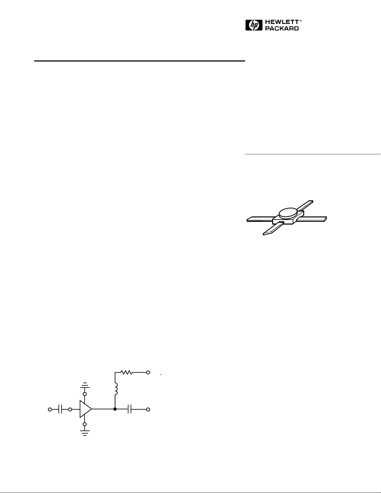
Typical Biasing Configuration
R
bias
100 mil Package
MAX
V
> 8 V
CC
RFC (Optional)
C
block
IN OUT
4
3
MSA
1
2
V
= 5.5 V
d
C
block
5965-9558E
6-462
Page 2
MSA-1110 Absolute Maximum Ratings
Parameter Absolute Maximum
Device Current 90 mA
Power Dissipation
RF Input Power +13 dBm
Junction Temperature 200°C
Storage Temperature –65 to 200° C
Notes:
1. Permanent damage may occur if any of these limits are exceeded.
2. T
3. Derate at 7.4 mW/°C for T
4. The small spot size of this technique results in a higher, though more
= 25°C.
CASE
accurate determination of θ
MENTS section “Thermal Resistance” for more information.
[2,3]
560 mW
> 124° C.
C
than do alternate methods. See MEASURE-
jc
[1]
Thermal Resistance
θjc = 135°C/W
[2,4]
:
Electrical Specifications
[1]
, T
= 25° C
A
Symbol Parameters and Test Conditions: Id = 60 mA, ZO = 50 Ω Units Min. Typ. Max.
G
∆G
f
P
3 dB
Power Gain (|S21|2) f = 0.1 GHz dB 11.5 12.5 13.5
Gain Flatness f = 0.1 to 1.0 GHz dB ±0.7 ± 1.0
P
3 dB Bandwidth
[2]
GHz 1.6
Input VSWR f = 0.1 to 1.0 GHz 1.7:1
VSWR
Output VSWR f = 0.1 to 1.0 GHz 1.9:1
NF 50 Ω Noise Figure f = 0.5 GHz dB 3.5 4.5
P
IP
t
V
1 dB
3
D
d
Output Power at 1 dB Gain Compression f = 0.5 GHz dBm 16.0 17.5
Third Order Intercept Point f = 0.5 GHz dBm 30.0
Group Delay f = 0.5 GHz psec 160
Device Voltage V 4.5 5.5 6.5
dV/dT Device Voltage Temperature Coefficient mV/°C –8.0
Notes:
1. The recommended operating current range for this device is 40 to 75 mA. Typical performance as a function of current
is on the following page.
Referenced from 50 MHz gain (GP).
2.
6-463
Page 3

MSA-1110 Typical Scattering Parameters (Z
G
p
(dB)
0.1.02 .05 0.5 1.0 2.0 3.0
FREQUENCY (GHz)
Figure 1. Typical Power Gain vs.
Frequency, I
d
= 60 mA.
4020 60 80
I
d
(mA)
Figure 3. Power Gain vs. Current.
0
2
4
6
8
10
14
12
16
4
6
8
12
10
14
G
p
(dB)
Figure 4. Output Power at 1 dB Gain
Compression, Noise Figure and Power
Gain vs. Case Temperature,
f = 0.5 GHz, I
d
= 60 mA.
3
4
5
11
13
12
16
17
18
–55 +25 +125
P
1 dB
(dBm)NF (dB)
Gp (dB)
TEMPERATURE (°C)
G
P
1.0 GHz,
P
1 dB
NF
20 468
V
d
(V)
Figure 2. Device Current vs. Voltage.
0
20
40
60
100
80
I
d
(mA)
TC = +125°C
T
C
= +25°C
T
C
= –55°C
FREQUENCY (GHz)
Figure 5. Output Power at 1 dB Gain
Compression vs. Frequency.
FREQUENCY (GHz)
Figure 6. Noise Figure vs. Frequency.
3.5
3.0
4.0
4.5
5.0
NF (dB)
0.1 0.2 0.3 0.5 2.01.0 0.1 0.2 0.3 0.5 2.01.0
12
14
16
18
22
20
P
1 dB
(dBm)
Id = 75 mA
Id= 75 mA
I
d
= 60 mA
I
d
= 40 mA
Id = 60 mA
Id = 40 mA
ZO = 50 Ω
Z
O
= 75 Ω
2.0 GHz
0.1 GHz
0.5 GHz
1.0 GHz
Freq.
S
11
S
21
= 50 Ω, TA = 25° C, I
O
S
12
S
= 60 mA)
d
22
GHz Mag Ang dB Mag Ang dB Mag Ang Mag Ang k
.0005 .83 –7 19.5 9.44 176 –31.9 .025 39 .84 –7 0.77
.005 .54 –50 16.8 6.92 158 –18.7 .116 34 .55 –50 0.60
.025 .15 –78 13.0 4.47 167 –16.6 .148 9 .15 –79 1.03
.050 .10 –64 12.6 4.26 171 –16.5 .149 5 .10 –67 1.08
.100 .08 –63 12.5 4.23 171 –16.5 .150 4 .08 –66 1.09
.200 .09 –74 12.4 4.17 166 –16.4 .152 4 .09 –78 1.09
.300 .11 –85 12.3 4.10 160 –16.2 .154 5 .12 –89 1.07
.400 .13 –94 12.3 4.10 154 –16.1 .157 6 .15 –98 1.05
.500 .16 –102 12.1 4.04 148 –15.9 .161 7 .18 –106 1.02
.600 .18 –108 12.0 3.98 143 –15.6 .165 8 .20 –113 1.00
.700 .21 –114 11.8 3.89 137 –15.4 .169 8 .23 –120 0.97
.800 .23 –120 11.6 3.80 131 –15.2 .173 8 .25 –126 0.95
.900 .25 –126 11.4 3.71 126 –15.0 .178 8 .28 –132 0.92
1.000 .27 –131 11.1 3.60 120 –14.8 .182 8 .30 –137 0.91
1.500 .36 –153 9.8 3.10 96 –13.8 .203 4 .37 –160 0.83
2.000 .42 –171 8.4 2.64 74 –13.3 .217 1 .40 –178 0.82
2.500 .47 177 7.2 2.29 59 –12.5 .236 –2 .41 172 0.80
3.000 .47 159 5.9 1.97 43 –13.2 .220 –10 .38 157 0.95
A model for this device is available in the DEVICE MODELS section.
Typical Performance, T
(unless otherwise noted)
= 25° C, ZO = 50␣ Ω
A
6-464
Page 4

100 mil Package Dimensions
.040
1.02
42GROUND
RF OUTPUT
RF INPUT
AND BIAS
.020
.508
1
.004 ± .002
.10 ± .05
.100
2.54
.495 ± .030
12.57 ± .76
GROUND
3
Notes:
(unless otherwise specified)
1. Dimensions are
2. Tolerances
in .xxx = ± 0.005
mm .xx = ± 0.13
.030
.76
in
mm
6-465
 Loading...