

Page 1
2-17
Features
• Mitel ST-BUS compatibl e
• 4-line x 32-c hanne l inpu ts
• 4-line x 32-c hanne l outpu ts
• 128 ports non-blocking switch
• Single power s upp ly (+5 V )
• Low power co nsu mpt ion: 30 m W Typ.
• Microprocess o r-c on t rol i nterface
• Three-state serial outputs
Description
This VLSI ISO-CMOS device is designed for
switching PCM-encoded voice or data, under
microprocessor control, in a modern digital
exchange, PBX or Central Office. It provides
simultaneous connections for up to 128 64 kbit/s
channels. Each of the four serial inputs and outputs
consist of 32 64 kbit/s channels multiplexed to form a
2048 kbit/s ST-BUS stream. In addition, the MT8981
provides microprocessor read and write access to
individual ST-BUS channels.
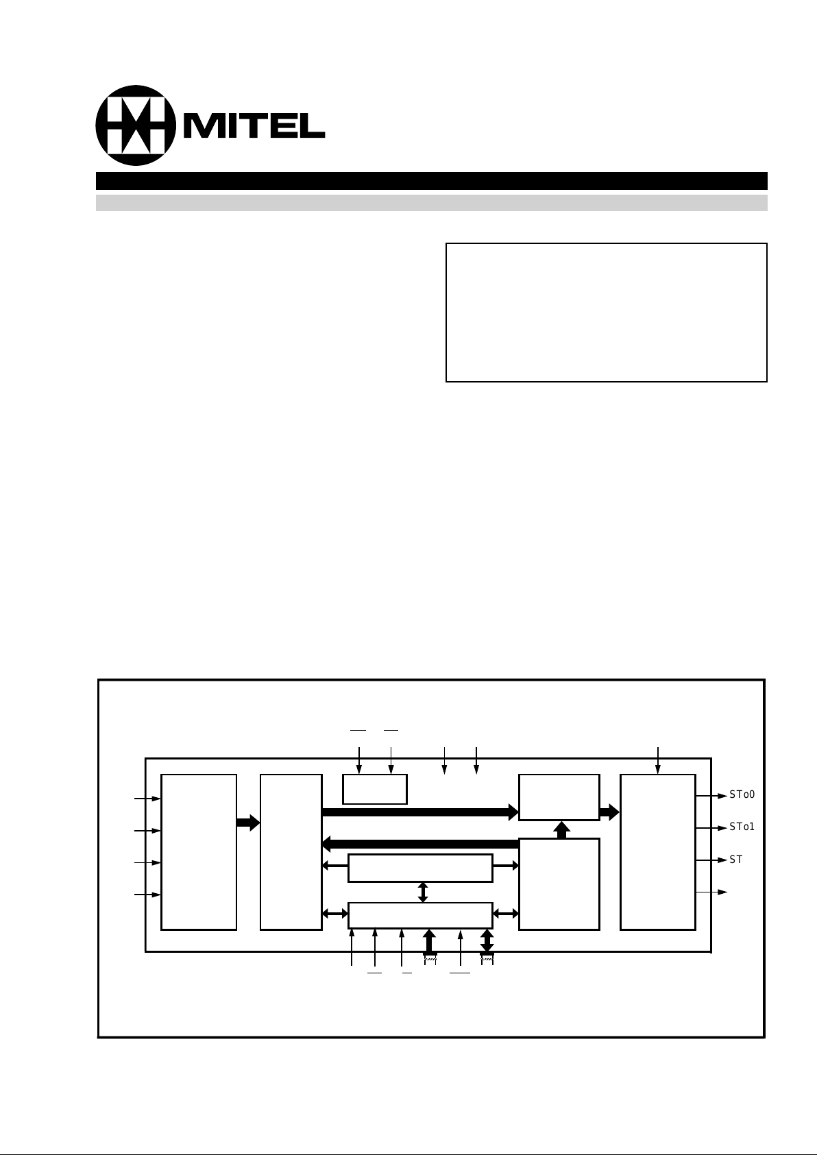
Figure 1 - Functional Block Diagram
STo0
STo1
STo2
STo3
Serial
to
Parallel
Converter
Data
Memory
Frame
Counter
Control Register
Control Interface
Output
MUX
Connection
Memory
Parallel
to
Serial
Converter
CS
R/W A5/A0DTA D7/
D0
C4i
F0i
VDDV
SS
ODE
STi0
STi1
STi2
STi3
DS
ISSUE 6 May 1995
MT8981D
Digital Switch
ISO-CMOS ST-BUS FA MILY
Ordering Information
MT8981DC 40 Pin Ceramic DIP
MT8981DE 40 Pin Plastic DIP
MT8981DP 44 PLCC
MT8981DL 44 Pin QFP
-40°C to +85°C
Page 2
MT8981D ISO-CMOS
2-18
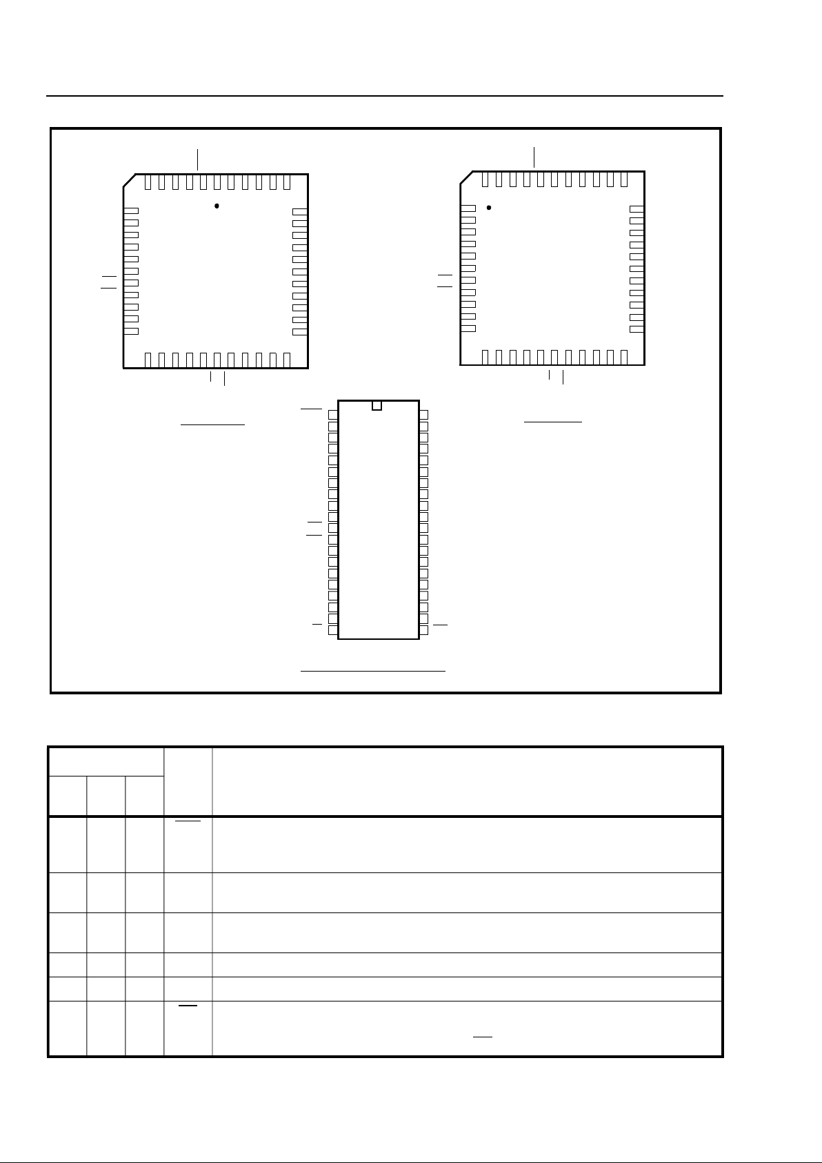
Figure 2 - Pin Connections
Pin Description
Pin #
Name Description
40
DIP44PLCC44QFP
1240DTAData Acknowledgemen t (Open Drai n Outpu t). This is the data a cknowledge men t
on the microprocessor interface. This pin is pulled low to signal that the chip has
processed the data. A 909 Ω, 1/4W, resistor is recommended to be used as a pullup.
2-4 3-5 41-43STi0-
STi2
ST-BUS Input 0 to 2 (Inputs). These are the inputs for the 2048 kbit/s ST-BUS input
streams.
571STi3ST-BUS Input 3 (Input). These are the inputs for the 2048 kbit/s ST-BUS input
streams.
6-9 8-11 2-5 IC Interna l Connecti on s. Must be connected to V
DD
.
10 12 6 V
DD
Power Input. Positive Supply .
11 13 7 F0i
Framing 0-Type (Input). This is the input for the frame synchronization pulse
for the 2048 kbit/s ST-BUS streams. A low on this input causes the internal counter
to reset on
the next negative transition of C4i.
1
65432
4443424140
7
8
9
10
11
12
13
14
15
16
39
38
37
36
35
34
33
32
31
30
23
1819202122
2425262728
17
29
STi3
IC
IC
IC
IC
VDD
F0i
C4i
A0
A1
A2
STo3
IC
IC
IC
IC
VSS
D0
D1
D2
D3
D4
NC
STi1
DTA
ODE
STo1
NC
NC
A4
DS
CS
D6
NC
A3
A5
R/W
D7
D5
44 PIN PLCC
DTA
STi0
STi1
STi2
STi3
IC
IC
IC
IC
VDD
F0i
C4i
A0
A1
A2
A3
A4
A5
DS
IC
ODE
STo0
STo1
STo2
STo3
IC
IC
IC
IC
VSS
D0
D1
D2
D3
D4
D5
D6
D7
CS
2
3
4
5
6
7
8
9
10
11
12
13
14
15
16
17
18
19
20
1
R/W
40
39
38
37
36
35
34
33
32
31
30
29
28
27
26
25
24
23
22
21
40 PIN CERDIP/PLASTIC DIP
STi2
STi0
IC
STo0
STo2
39
4443424140
3837363534
1
2
3
4
5
6
7
8
9
10
33
32
31
30
29
28
27
26
25
24
17
1213141516
1819202122
11
23
44 PIN QFP
STi3
IC
IC
IC
IC
VDD
F0i
C4i
A0
A1
A2
NC
A4
DS
CS
D6
NC
A3
A5
R/W
D7
D5
STo3
IC
IC
IC
IC
VSS
D0
D1
D2
D3
D4
NC
STi1
DTA
ODE
STo1
NC
STi2
STi0
IC
STo0
STo2
Page 3
ISO-CMOS MT8981D
2-19
12 14 8 C4i 4. 096 MHz Clo ck (In put). ST-BUS bit cell boundaries lie on the alternate falling
edges of this clock.
13-1515-179-11 A0-A2 Address 0 to 2 (Inputs). These are the inputs for the addre ss lines on the
microprocessor interface.
16-1819-2113-15A3-A5 Address 3 to 5 (Inp uts). These are the inputs for the addre ss lines on the
microprocessor interface
19 22 16 DS Data Strobe (Inpu t). This is the input f or the active hig h data strobe on the
microprocessor interface.
20 23 17 R/W
Read or Write (Input). Th is is the input for the read/write signal on the
microprocessor interface - high for read, low for write.
21 24 18 CS
Chip Select (Inp ut). This is the input for the acti ve low chip select on the
microprocessor interface.
22-2425-2719-21D7-D5 Data 7 to 5 (Three-state I/O Pins). These are the bidirectional data pins on the
microprocessor interface.
25-2929-3323-27D4-D0 Data 4 to 0 (Three-state I/O Pins). These are the bidirectional data pins on the
microprocessor interface.
30 34 28 V
SS
Power Input. Negative Supply (Ground).
31-3435-3829-32IC Interna l Connec tions. Leave pins disconnected.
35 39 33 STo3 ST-BUS Output 3 (Three-state Outputs). These are the pins for the four 2048 kbit/s
ST-BUS output streams.
36-3841-4335-37STo2-
STo0
ST-BUS Output 2 to 0 (Three-state Outputs). These are the pins for the four 2048
kbit/s ST-BUS output streams.
39 44 38 ODE Output Drive Enabl e (In put). If this input is held high, the ST o0-STo3 output drivers
function normall y. If this input is low, the STo0-STo3 out put drivers go into thei r high
impedance state. NB: Even when ODE is high, channe ls on the STo 0-STo3 outputs
can go high impedance under software control.
40 1 39 IC Internal Connec tion. Leave pin disconnect e d.
Pin Description (continued)
Pin #
Name Description
40
DIP44PLCC44QFP
Page 4
MT8981D ISO-CMOS
2-20
Functional Description
In recent years, there has been a trend in telephony
towards digital switching, particularly in association
with software control. Simultaneously, there has
been a trend in system architectures towards
distributed processing or multi-processor systems.
In accordance with these trends, MITEL has devised
the ST-BUS (Serial Telecom Bus). This bus
architectur e can be used both i n software-contr olled
digital voice and data switching, and for
interprocessor communications. The uses in
switching and in interprocessor communications are
completely integrated to allow for a simple general
purpose architecture appropriate for the systems of
the future.
The serial streams of the ST-BUS operate
continuously at 2048 kbit/s and are arranged in 125
µs wide frames which contain 32 8-bit channels.
MITEL manufactures a number of devices which
interface to the ST-BUS; a key device being the
MT8981 chip.
The MT8981 can switch data from channels on STBUS inputs to channels on ST-BUS outputs, and
simultaneously allows its controlling microprocessor
to read channels on ST-BUS inputs or write to
channels on ST-BUS outputs (Message Mode). To
the microprocessor, the MT8981 looks like a memory
peripheral. The microprocessor can write to the
MT8981 to establish switched connections between
input ST-BUS channels and output ST-BUS
channels, or to transmit messages on output STBUS channels. By reading from the MT8981, the
microprocessor can receive messages from ST-BUS
input channels or check which switched connections
have already been established.
By integrating both switching and interprocessor
communications, the MT8981 allows systems to use
distributed processing and to switch voice or data in
an ST-BUS architecture.
Hardware Descr iption
Serial data at 2048 kbit/s is received at the four STBUS inputs (STi0 to STi3), and serial data is
transmitted at the four ST-BUS outputs (STo0 to
STo3). Each serial input accepts 32 channels of
digital data, each channel containing an 8-bit word
which may represent a PCM-encoded analog/voice
sample as provided by a codec (e.g., MITEL’s
MT8964).
This serial input word is converted into parallel data
and stored in the 128 X 8 Data Memory. Locations in
the Data Memory are associated with particular
channels on particular ST-BUS input streams.
These locations can be read by the microprocessor
which controls the chip.
Locations in the Connection Memory, which is split
into high and low parts, are associated with
particular ST-BUS output streams. When a channel
is due to be transmitted on an ST-BUS output, the
data for the channel can either be switched from an
ST-BUS input or it can originate from the
microprocessor. If the data is switched from an
input, then the contents of the Connection Memory
Low location associated with the output channel is
used to address the Data Memory. This Data
Memory address corresponds to the channel on the
input ST-BUS stream on which the data for switching
arrived. If the data for the output channel originates
from the microprocessor (Message Mode), then the
contents of the Connection Memory Low location
associated with the output channel are output
directly, and this data is output repetitively on the
channel once every frame until the microprocessor
intervenes.
The Connection Memory data is received, via the
Control In terface, at D7 to D0. Th e Contr ol Interface
also receives address information at A5 to A0 and
handles the microprocessor control signals CS
,
DTA
, R/W and DS. There are two parts to any
address in the Data Memory or Connection
Memory. The higher order bits come from the
Figure 3 - Address Memory Map
A5 A4 A3 A2 A1 A0 H EX ADDRESS LOCATI ON
0
1
1
•
•
•
1
X
0
0
•
•
•
1
X
0
0
•
•
•
1
X
0
0
•
•
•
1
X
0
0
•
•
•
1
X
0
1
•
•
•
1
00 - 1F
20
21
•
•
•
3F
Control Register *
Channel 0
†
Channel 1
†
•
•
•
Channel 31
†
* Writing to the Control Register is the only fast transaction.
† Memory and stream are specified by the content s of the Control Regist er.
Page 5
ISO-CMOS MT8981D
2-21
Control Register, which may be written to or read
from via the Control Interface. The lower order bits
come from the address lines directly.
The Control Register also allows the chip to
broadcast messages on all ST-BUS outputs (i.e., to
put every channel into Message Mode), or to split the
memory so that reads are from the Data Memory and
writes are to the Connection Memory Low. The
Connection Memory High determines whether
individual output channels are in Message Mode,
and allows individual output channels to go into a
high-impedance state, which enables arrays of
MT8981s to be constructed. It also controls the
CSTo pin.
All ST-BUS timing is derived from the two
signals C4i
and F0i.
Software Control
The address lines on the Control Interface give
access to the Control Regis ter directly or, depending
on the co ntents of the Control Regi ster, to the High
or Low sections of the Connection Memory or to the
Data Mem o ry.
If address line A5 is low, then the Control Register is
addressed regardless of the other address lines (see
Fig. 3). If A5 is high, then the address lines A4-A0
select the mem ory location corresponding to channel
0-31 for the memory and stream selected in the
Control Register.
The data in the Control Register consists of mode
control bits, memory select bits, and stream address
bits (see Fig. 4). The memory select bits allow the
Connection Memory High or Low or the Data
Memory to be chosen, and the stream address bits
define one of the ST-BUS input or output streams.
Bit 7 of the Control Register allows split memory
operation - reads are from the Data Memory and
writes are to the Connection Memory Low.
The other mode control bit , bit 6, puts every output
channel on every output stream into active Message
Mode; i.e., the contents of the Connection Memory
Low are output on the ST-BUS output streams once
every frame unless the ODE pin is low. In this mode
the chip behaves as if bits 2 and 0 of every
Connection Memory High location were 1, regardless
of the actual valu es.
Figure 4 - Control Register Bits
BIT NAME DESCRIPTION
7 Split
Memory
When 1, all subsequent reads are from the Data Memory and writes are to the Connection
Memory Low, except when the Control Register is accessed again. When 0, the Memory
Select bits specify the memory for subsequent operati ons. I n either case, the Stream
Address Bits select the subsection of the memory which is made avail able.
6 Message
Mode
When 1, the contents of the Connection Mem or y Low are output on the Serial Output
streams except when the ODE pin is low. When 0, the Connection Memory bits for each
channel determine what is output.
5 (unused)
4-3 Memory
Select Bits
0-0 - Not to be used
0-1 - Data Memory (read only from the microprocessor port)
1-0 - Connection Memory Low
1-1 - Connection Memory High
2 (unused) Must be a 0.
1-0 Stream
Address
Bits
The number expressed in binary notation on these bit s refers to the input or outpu t STBUS stream which corresponds to the subsection of memory made accessible for
subsequent operations.
76 5432 10
Mode
Control
Bits
(unused) Memory
Select
Bits
Stream
Address
Bits
(unuse d)
Page 6
MT8981D ISO-CMOS
2-22
Figure 5 - Connection Memory High Bits
Figure 6 - Connection Memory Low Bits
BIT NAME DESCRIPTION
2 Message
Channel
When 1, the contents of the corresponding location in Connection Memory Low are
output on the location’s channel and stream. When 0, the contents of the corresponding
location in Connection Memory Low act as an address for the Data Mem ory and so
determine the source of the connection to the location ’s channel and stream.
1 Unused
0 Output
Enable
If the ODE pin is high and bit 6 of the Control Register is 0, then this bit enables the
output driver for the location’s channel and stream. This allows individua l channels on
individual streams to be made high-im ped ance, all owing swit ching matrices to be
constructed. A 1 enables the driver and a 0 disables it.
BIT NAME DESCRIPTION
7 (Unused) Must be a 0.
6-5* Stream
Address
Bits*
The number expressed in binary notation on these 2 bits is the number of the ST-BUS
stream for the source of the connection. Bit 6 is the most significan t bit. e.g., if bit 6 is 1,
and bit 5 is 0, then the source of the connection is a channel on STi2.
4-0* Ch annel
Address
Bits*
The number expressed in binary notation on these 5 bits is the number of the channel
which is the source of the connection (The ST-BUS stream where the channel lies is
defined by bits 6 and 5.). Bit 4 is the most significant bit. e.g., if bit 4 is 1, bit 3 is 0, bit 2 is
0, bit 1 is 1 and bit 0 is 1, then the source of the connection is channel 19.
*If bit 2 of the corresponding Connection High location is 1 or if bit 6 of the Control Register is 1, then these entire
8 bits are output on the channel and stream associated with this location. Otherwi se, the bits are used as
indicated to define the source of the connection which is output on the channel and stream associat ed wit h this
location.
76 5432 10
No Corresponding Memory
- These bits give 0s if read.
Per Channel
Control Bits
76 5432 10
76 5432 10
(unused) Stream
Address
Bits
Channel
Address
Bits
Page 7

ISO-CMOS MT8981D
2-23
If bit 6 of the Control Register is 0, then bits 2 and 0
of each Connection Memory High location function
normally (see Fig. 5). If bit 2 is 1, the associated STBUS output channel is in Message Mode; i.e., the
byte in the corresponding Connection Memory Low
location is transmitted on the s tream at that channel.
Otherwise, one of the bytes received on the serial
inputs is transmitted and the contents of the
Connection Memory Low define the ST-BUS input
stream and channel where the byte is to be found
(see Fig. 6).
If the ODE pin is low, then all serial outputs are highimpedance. If it is high and bit 6 in the Control
Register is 1, then all outputs are active. If the ODE
pin is high and bit 6 in the Control Register is 0, then
the bit 0 in the Connection Memory High location
enables the output drivers for the corresponding
individual ST-BUS output stream and channel. Bit
0=1 enables the driver and bit 0=0 disables it (see
Fig. 5).
Applications
Use in a Simple Digital Switching System
Fig. 7 and 8 show how MT8981s can be used with
MT8964s to form a simple digital switching system.
Fig. 7 shows the interface betwe en the MT8981s and
the filter/codecs. Fig. 8 shows the position of these
components in an example architecture.
The MT8964 filter/codec in Fig. 7 receives and
transmits digitised voice signals on the ST-BUS input
D
R
, and ST-BUS output DX, respectively. These
signals are routed to the ST-B US inputs and outputs
on the top MT8981, which is used as a digital speech
switch.
The MT8964 is controlled by the ST-BUS input D
C
originating from the bottom MT8981, which
generates the appropriate signals from an output
channel in Message Mode. This architecture
optimises the messaging capability of the line circuit
by building signalling logic, e.g., for on-off hook
detection, which communicates on an ST-BUS
output. This signalling ST-BUS output is monitored
by a microprocessor (not shown) through an ST-BUS
input on the bot tom MT8981.
Fig. 8 shows how a simple digital switching system
may be designed using the ST-BUS architecture.
This is a private telephone network with 128
extensions which uses a single MT8981 as a speech
switch and a second MT8981 for communication with
the line interface circuit s.
A larger digital switching system may be designed by
cascading a number of MT8981s. Fig. 9 shows how
four MT8981s may be arranged in a non-blocking
configurat ion which can switch any channel on any
of the ST-BUS inputs to any channel on the ST-BUS
outputs.
Figure 7 - Example of Typical Interface between 8981s and 8964s for Simple Digital Switch ing System
8981 used
as
speech
switch
MT8981
STo0
STi0
STo0
STi0
MT8981
8981 used
in message
mode for
control and
signalling
D
X
D
R
D
C
MT8964
Filter/Codec
Signalling
Logic
Line Driver
and
2- to 4-
Wire
Converter
Line Interface Circuit with 8964 Filter/Codec
Page 8

MT8981D ISO-CMOS
2-24
Figure 8 - Ex amp le Arch itec ture o f a Simp le Dig ital Swi tchin g S ystem
Controlling
Micro-
Processor
Speech
Switch
-
8981
Control &
Signalling
-
8981
STo0-3
STi0-3
STo0-3
Line Interface Circuit
with Codec (e.g. 8964)
Line 1
Line 128
Line Interface Circuit
with Codec (e.g. 8964)
4
4
4
4
•
•
•
Repeated for Lines
2 to 127
•
•
•
Repeated for Lines
2 to 127
STi0-3
Applicatio n Circui t with 680 2 Pr ocess or
Fig. 10 shows an example of a complete circuit
which may be used to evaluate the chip.
For convenience, a 4 MHz crystal oscillator has been
used rather than a 4.096 MHz clock, as both are
within the limits of the chip’s specifications. The RC
delay used with the 393 counters ensures a
sufficient hold time for the FP
signal, but the values
used may have to be changed if faster 393 counters
become available.
The chip is shown as memory mapped into the
MEK6802D3 system. Chip addresses 00-3F
correspond to processor addresses 2000-203F.
Delay through the address decoder requires the
VMA signal to be used twice to remove glitches. The
MEK6802D3 board uses a 10KΩ pullup on the MR
pin, which would have to be incorporated into the
circuit if the board was replaced by a processor.
Figure 9 - Four 8981s Arrange d in a Non-Blocking 8 x 8 Configuration
IN 0/3
IN 4/7
8981
#1
STi0/3 STo0/3
8981
#2
STi0/3 STo0/3
8981
#3
STi0/3 STo0/3
8981
#4
STi0/3 STo0/3
OUT 0/3
OUT 4/7
Page 9

ISO-CMOS MT8981D
2-25
Figure 10 - Application Circuit with 6802
MEK6802D3
System
D7-D0
A15-A0
R/W
MR
VMA
E
A15
A14
A13
0V
0V
VMA
0V
5V
5V
5V
A12
A11
A10
0V
0V
0V
0V
0V
A9
A8
A7
0V
0V
A6
VMA
0V
0V
0V
1
2
3
4
5
6
7
8
16
15
14
13
12
11
10
9
1
2
3
4
5
6
7
8
16
15
14
13
12
11
10
9
1
2
3
4
5
6
7
8
16
15
14
13
12
11
10
9
1
2
3
4
5
6
7
8
16
15
14
13
12
11
10
9
5V
1
2
3
4
5
6
7
8
20
19
18
17
16
15
14
13
9
10
12
11
MD
74
HCT
138
MD
74
HCT
138
MD
74
HCT
138
MD
74
HCT
138
MD
74
HCT
240
DTA
CS
0V
C4i
0V
F0i
0V
0V
5V
0V
MR
4 MHz
2MΩ
1
2
3
4
5
6
7
14
13
12
11
10
9
8
5V
5V
0V
C4i
0V
0V
0V
0V
SN
74
HCT
393
SN
74
HCT
393
909 Ω,
1/4W
MT
8981
DTA
STi0
STi1
STi2
STi3
VDD
F0i
C4i
A0
A1
A2
A3
A4
A5
DS
R/W
1
2
3
4
5
6
7
8
9
10
11
12
13
14
15
16
17
18
19
20
40 CSTo
ODE
STo0
STo1
STo2
STo3
VSS
D0
D1
D2
D3
D4
D5
D6
D7
CS
39
38
37
36
35
34
33
32
31
30
29
28
27
26
25
24
23
22
21
5V
0V
5V
5V
510 Ω
100pF
5V
1
2
3
4
5
6
7
14
13
12
11
10
9
8
Page 10

MT8981D ISO-CMOS
2-26
* Exceeding these values ma y cause perm anen t dama ge. Functi onal operati on und er these cond ition s is not implied.
.
‡ Typ ical figures are at 25 °C and are for design aid only: not guaranteed and not subject to production testing.
‡ Typ ical figures are at 25 °C and are for design aid only: not guaranteed and not subject to production testing.
Figure 11 - Output Test Load
Absolute Maximum Ratings*
Parameter Symbol Min Max Units
1V
DD
- V
SS
-0.3 7 V
2 Voltage on Digital Inputs V
I
VSS-0.3 VDD+0.3 V
3 Voltage on Digital Output s V
O
VSS-0.3 VDD+0.3 V
4 Curren t at Digital Outputs I
O
40 m A
5 Storage Tem perat ure T
S
-65 +150 °C
6 Package Power Dissipation P
D
2W
Recommended Operating Conditions - Voltages are with respect to ground (V
SS
) unless otherwise stated.
Characteristics Sym Min Typ
‡
Max Units Test Conditions
1 Operating Temperature T
OP
-40 +85 °C
2 Positive Supply V
DD
4.75 5.25 V
3 Input Voltage V
I
0V
DD
V
DC Electrical Characteristics - Voltages are with respect to ground (V
SS
) unless otherwise stated.
Characteristics Sym Min Typ‡Max U n its Test Conditions
1
I
N
P
U
T
S
Supply Current I
DD
6 10 m A Outputs unloaded
2 Input High Voltage V
IH
2.0 V
3 Input Low Voltage V
IL
0.8 V
4 Input Leakage I
IL
5 µAVI between VSS and V
DD
5 Input Pin Capacitance C
I
8pF
6
O
U
T
P
U
T
S
Output High Voltage V
OH
2.4 V IOH = 10 mA
7 Output High Current I
OH
10 15 mA Sourcing. VOH=2.4V
8 Output Low Voltage V
OL
0.4 V IOL = 5 mA
9 Output Low Current I
OL
5 10 mA Sinking. VOL = 0.4V
10 High Impedance Leakage I
OZ
5 µAVO between VSS and V
DD
11 Output Pin Capacitance C
O
8pF
Output
Pin
Test Point
C
L
V
SS
S1
R
L
V
DD
S2
V
SS
S1 is open circuit except
when testing output levels
or high impedance states.
S2 is switched to V
DD
or
V
SS
when te st i ng output
levels or high impedance
states.
Page 11

ISO-CMOS MT8981D
2-27
† Timing is over recommended temperature & power supply voltages
‡ Typical figures are at 25°C and are for design aid only: not guaranteed and not subject to producti on testin g.
* Contents of Connectio n Memory are not lost if the clock stops, however, ST-BUS outputs go into the high impedance state.
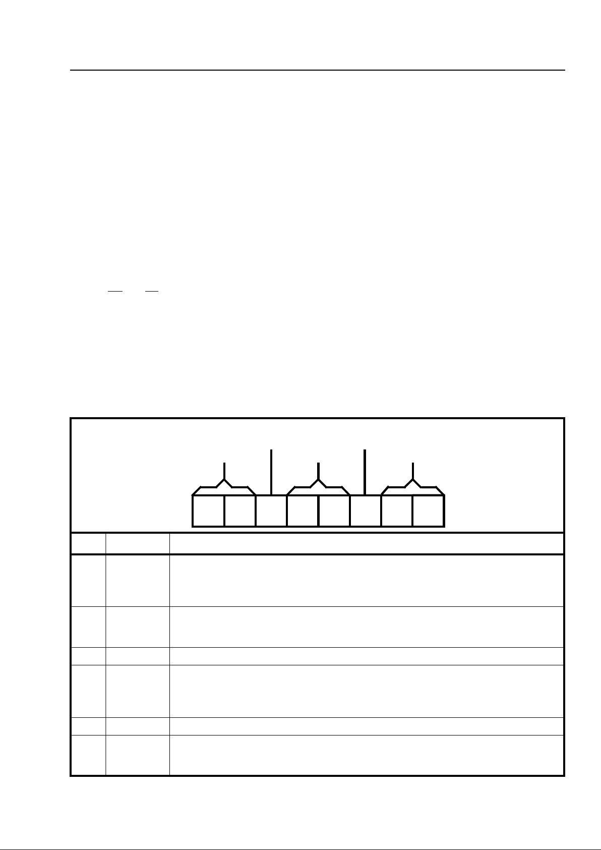
NB: Frame Pulse is repeated every 512 cycles of C4i
.
Figure 12 - F rame Al ignm ent
Figure 13 - Clock Timing
AC Electrical Characteristics† - Clock Tim i ng (Figures 12 and 13)
Characteristics Sym Min Typ‡Max Units Test Conditions
1
I
N
P
U
T
S
Clock Period* t
CLK
220 244 300 ns
2 Clock Width High t
CH
95 12 2 150 ns
3 Clock Width Low t
CL
110 122 150 ns
4 Clock Transitio n Time t
CTT
20 ns
5 Frame Pulse Setup Time t
FPS
20 200 ns
6 Frame Pulse Hold Time t
FPH
0.020 50 µs
7 Frame Pulse Width t
FPW
244 ns
t
CLK
t
CTT
t
CH
t
CHL
t
CTT
t
FPH
t
FPS
t
FPH
t
FPS
t
FPW
t
CL
C4i
F0i
2.0V
0.8V
2.0V
0.8V
C4i
F0i
BIT
CELLS
Channel 31
Bit o
Channel 0
Bit 7
Page 12

MT8981D ISO-CMOS
2-28
† Timing is over recommended temperature & power supply voltages
‡ Typical figures are at 25°C and are for design aid only: not guaranteed and not subject to producti on testin g.
* High Impedance is measured by pulling to the appropriate rail with R
L
, with timing corrected to cancel time taken to discharge CL.
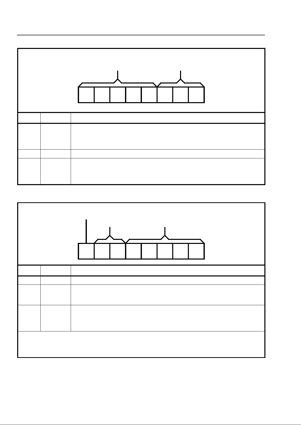
AC Electrical Characteristics† - Serial Streams (Figures 11, 14, 15 and 16)
Characteristics Sym Min Typ‡Max Units Test Conditions
1
O
U
T
P
U
T
S
STo0/3 Delay - Active to High Z t
SAZ
20 50 80 ns RL=1 KΩ*, CL=150 pF
2 STo0/3 Delay - High Z to Active t
SZA
25 60 125 ns CL=150 pF
3 STo0/3 Delay - Active to Active t
SAA
30 65 125 ns CL=150 pF
4 STo0/3 Hold Time t
SOH
25 45 ns CL=150 pF
5 O utp ut Driver Enable Delay t
OED
45 125 ns RL=1 KΩ*, CL=150 pF
6 Ext ernal Cont ro l Hold Time t
XCH
050 nsC
L
=150 pF
7 Ext ernal Cont ro l Delay t
XCD
75 110 ns CL=150 pF
8
I
N
Serial Input Setup Time t
SIS
-40 -20 ns
9 Serial Input Hold Time t
SIH
90 ns
Figure 14 - Serial Outputs and External Control
C4i
2.0V
0.8V
STo0
to
STo3
2.4V
0.4V
STo0
to
STo3
2.4V
0.4V
STo0
to
2.4V
0.4V
Bit Cell Boundary
STo3
t
SOH
t
SAZ
t
SZA
t
SOH
t
SAA
*
*
Figure 15 - Output Driver Enable
Figure 16 - Serial Inputs
Bit Cell Boundaries
C4i
2.0V
0.8V
2.0V
0.8V
t
SIS
t
SIH
STi0
to
STi3
ODE
2.0V
0.8V
STo0
to
STo3
2.4V
0.4V
*
t
OED
t
OED
*
Page 13

ISO-CMOS MT8981D
2-29
† Timing is over recommended temperature & power supply voltages.
‡ Typical figures are at 25°C and are for design aid only: not guaranteed and not subject to producti on testin g.
* High Impedance is measured by pulling to the appropriate rail with R
L
, with timing corrected to cancel time taken to discharge CL.
➀ Proce ss o r a c ces s es a re depend en t o n the C 4 i c lo c k, an d so s om e tim i ng s ar e ex p res s ed as m u lti pl es o f the C4i clock period.
Figure 17 - Proc esso r Bus
AC Electrical Characteristics† - Processor Bus (Figures 11 and 17)
Characteristics Sym Min Typ
‡
Max Units Test Co nditions
1 Chip Select Setup Time t
CSS
20 0 ns
2 Read/Write Setup Time t
RWS
25 5 ns
3 Address Setup Time t
ADS
25 5 ns
4 Acknowledgement Delay Fast
Slow
t
AKD
40 100 ns CL=150 pF
t
AKD
2.7 7.2 cycles C4i cycles
➀
5 Fast Write Data Setup Time t
FWS
20 ns
6 Slow Write Data Delay t
SWD
2.0 1.7 cycles C4i cycles
➀
7 Read Data Setup Time t
RDS
0.5 cycles C4i cycles➀, CL= 150 pF
8 Data Hold Time Read
Write
t
DHT
20 ns RL=1 KΩ∗, CL=150 pF
t
DHT
20 10 ns
9 Read Data To High Impedance t
RDZ
50 90 ns RL=1 KΩ∗, CL=150 pF
10 Chip Select Hold Time t
CSH
0ns
11 Read/Write Hold Time t
RWH
0ns
12 Address Hold Time t
ADH
0ns
13 Acknowledgement Hold Time t
AKH
10 60 80 ns RL=1 KΩ∗, CL=150 pF
DS
2.0V
0.8V
2.0V
0.8V
2.0V
0.8V
2.0V
0.8V
2.4V
0.4V
2.4V (Read) 2.0V (Write)
0.8V (Read 0.8V (Write)
CS
R/W
A5
DTA
D7
t
CSS
t
RWS
t
ADS
t
AKD
t
RDS
t
SWD
t
FWS
t
CSH
t
RWH
t
ADH
t
AKH
t
DHT
*
*
*
*
t
RDZ
to
A0
to
D0
Page 14

MT8981D ISO-CMOS
2-30
NOTES:
 Loading...