

Page 1

Application SpecificDiscretes
A.S.D.
FEATURES
SPACE SAVING :MONOLITHIC FIRE LIGHTER
FUNCTION INTEGRATION
DEDICATED THYRISTOR STRUCTURE FOR
CAPACITANCE DISCHARGE IGNITION
OPERATION
TM
FLC02-200D
FIRE LIGHTER CIRCUIT
HIGH PULSECURRENT CAPABILITY
150A @ tp = 10µs
DESCRIPTION
The FLC02 is a high performance planar dif-
-
fused technology adapted to high temperature
and rugged environmentalconditions.
It has been developed especially for capaci-
-
tance discharge operation. The main applications are ignitorcircuitssuch as :
fuel ignitiors / gasboilers...
Th : Thyristor for switchingoperation.
Z : Zener diode to set the thresholdvoltage.
D : Diode for reverseconduction.
R : 2 kOhm resistor.
1
2
3
SOT82
(Plastic)
FUNCTIONAL DIAGRAM
Z
pin 3
R
pin 2
Th
D
February 1996
pin 1
1/7
Page 2

FLC02-200D
ABSOLUTE RATINGS (limiting values) : 0°C<T
amb
<90°C
Symbol Parameter Value Unit
I
TRM
I
FRM
I
TSM
Repetitivesurgepeakonstatecurrentforthyristor tp =10µs
Repetitivesurgepeakonstatecurrentfordiode
( note 1)
150 A
Non repetitivesurgepeakonstate current tp =10ms 5 A
di/dt Criticalrateof rise time on statecurrent 120 A/µs
T
stg
Tj
Toper
T
L
Storage junction temperaturerange
Maximumjunctiontemperature
Operatingtemperaturerange
Maximumleadtemperaturefor solderingduring10s 260 °C
- 40 to+150
+ 125
0+90 °C
Note 1 : Test currentwaveform
°C
µ
10 s
200ms
THERMAL RESISTANCE
Symbol Parameter Value Unit
R
th(j-a)
Thermalresistance junctionto ambient 100 °C/W
ORDERINGINFORMATION
FLC 02 - 200 D
FIRE LIGHTERCIRCUIT
PACKAGED: SOT82
2/7
CIRCUIT NUMBER : 02 =scr + diode + zener + resistance
(gate connectedto pin 3)
V
RM
200= 200 V
Page 3
FLC02-200D
ELECTRICAL CHARACTERISTICS
Symbol Parameters
V
RM
V
BO
V
T
V
F
I
RM
I
BO
Stand-offvoltage
Breakovervoltage
On-statevoltagedrop
Diodevoltagedrop
Leakage current
Breakovercurrent
V
BO
V
RM
I
I
F
V
T
I
RM
I
BO
I
BO
I
V
F
1
2
T
DIODE (D) PARAMETER
Symbol Test Conditions Value Unit
V
F
IF=2A tp≤1ms Tj=25°C MAX 1.7 V
THYRISTOR(Th) and ZENER (Z) PARAMETERS
V
Symbol Testconditions Value Unit
I
RM
VRM=200V Tj = 25°CMAX 10 µA
Tj =120°C MAX 100 µA
V
BO
I
1atVBOPin3 (gate) open Tj = 25°C MAX 0.5 mA
BO
I
2atVBOPin1( c athode)and pin3(gate)in c/c Tj = 25°C MIN 40 mA
BO
V
T
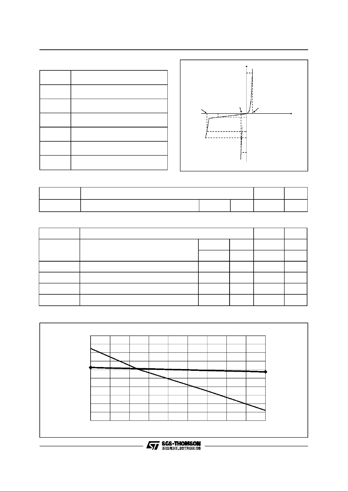
Fig.1 : Relative variationof breakovercurrent(I
at I
Pin3 (gate) open Tj = 25°C MAX 250 V
BO1
IT=2A tp≤1ms Tj = 25°C MAX 1.7 V
) versus junction temperature
BO
Ibo (Tj) / Ibo (25°C)
1.4
1.2
1
IbO2
0.8
IbO1
0.6
0.4
020406080
Tj (°C)
3/7
Page 4

FLC02-200D
BASIC APPLICATION
Rs DTs
AC
MAINS
Ic
Ic
t
c
Th
Z
D
Sensor
The applications of the FLC02 using the capacitance discharge topologyoperatein2modes:
- Ignitionmode: TransistorTisOFF
- Blankingmode: TransistorT is ON
1) IGNITION MODE(TransistorT
OFF
)
PHASE1:
The energy coming from the mains is stored into
the capacitorC. Forthat, the AC voltageisrectified
by thediode Ds.
PHASE2 :
At the end of the phase 1, the voltage across the
capacitor C reaches the avalanche threshold of
the zener.Then a currentflows throughthegateof
the thyristorTh which fires.
The firingofthethyristorcauses analternatingcurrent to flow through the capacitorC.
The positivepartsofthiscurrentflowthroughC,Th
and the primary of the HV transformer.
The negativeparts of the currentflowthroughC,D
and the primary of the HV transformer.
R
RS RESISTOR CALCULATION
The Rs resistorallows,in addition withthe capacitor C, to adjustthe sparkfrequencyandto limitate
the current from the mains. Its value shall allow
the thyristor Th to fire even in the worst case. In
this borderline case the system must fire with the
lower RMS mains voltage value while the breakdown voltage and current of the FLC are at the
maximum.
The maximumRs valueis equal to :
V
Rs
max =
minx√2 )−
(
AC
I
BO
1
max
V
BO
max
4/7
Page 5

Fig2. : Spark frequency versusRs and C
F (Hz)
20
FLC02-200D
C=0.47µF
10
C=3.3µF
C=2.7µF
C=1.5µF
C=2.2µF
C=1µF
5
3
2
6111621
Rs (kOhms)
The coupleRs/C can be chosen withthe previous
curve. Keep in mind the Rs maximum limit for
which the system would not work when the AC
Fig. 3 : Voltageacross the capacitance with Rs = 15 kOhmsand C = 1µF
mains is minimum.
The next curve shows the behavior with
Rs=15kOhmsandC=1µF.
5/7
Page 6

FLC02-200D
PEAK CURRENT LIMIT
This compo nent is designed to withstand
Ip = 150Aforapulsedurationof10µsforan ambient temperatureof 90°C.
Fig. 4 :Peak current limit
Ip (A)
190
180
170
160
150
140
130
120
The curve of peak current versus the pulse durationallowsustoverifyiftheapplicationiswithinthe
FLC operating limit.
110
6 8 10 12 14
t(µs)
POWER LOSSES (For 10µs, see note 1)
To evaluatethepower losses, please usethefollowing equations :
For the thyristor: P = 1.18 x I
For the diode : P = 0.67 x I
F(AV)
T(AV)
+0.106I
+0.035I
2/ BLANKING MODE (Transistor TON)
In thismodeandtransistorTis saturatedandstops
the sparkgeneration.
Rs (kohms)
100
80
60
40
20
2
2
F(RMS)
T(RMS)
In order to keep the thyristor Th in blanking mode
and becauseofthepower dissipation,theResistor
(Rs) has to keep a minimum value of 22 kΩ (see
next curve) :
Rs max
Rs min
6/7
0
0 20406080100120
Tamb(°C)
Vac= 220V +15%
-10%
Page 7

PACKAGEMECHANICAL DATA
SOT82 (Plastic)
FLC02-200D
CA
REF.
Millimeters Inches
DIMENSIONS
Min. Max. Min. Max.
B
A 7.4 7.8 0.291 0.307
B 10.5 10.8 0.413 0.425
C 2.4 2.7 0.094 0.106
H
D 0.7 0.9 0.027 0.035
E 2.2 typ. 0.087typ.
L
D
M
F
E
G
F 0.49 0.75 0.019 0.029
G 4.15 4.65 0.163 0.183
H (1) 2.54 0.100
L 15.7 typ. 0.618 typ.
M 1.0 1.3 0.039 0.051
(1) Within this region the cross-section of the
leads isuncontrolled
Markingtype number
Weight: 0.72g.
Information furnished is believed tobe accurate and reliable. However, SGS-THOMSON Microelectronics assumes no responsability for the
consequences of use of such information nor for any infringement of patents or other rights of third parties which may result from its use. No
license is granted by implication or otherwise under anypatentorpatent rightsofSGS-THOMSONMicroelectronics. Specifications mentioned
in this publication are subjectto change without notice.Thispublication supersedes and replaces all informationpreviously supplied.
SGS-THOMSON Microelectronicsproducts arenotauthorized foruse ascritical components inlife support devicesor systems without express
written approval of SGS-THOMSON Microelectronics.
1996 SGS-THOMSON Microelectronics -Printedin Italy- All rights reserved.
SGS-THOMSON Microelectronics GROUPOF COMPANIES
Australia - Brazil - Canada - China - France - Germany - Hong Kong- Italy - Japan - Korea - Malaysia - Malta - Morocco -
The Netherlands -Singapore - Spain - Sweden - Switzerland - Taiwan - Thailand- United Kingdom - U.S.A.
7/7
 Loading...