

Page 1
www.fairchildsemi.com
AN-9744
Smart LED Lamp Driver IC with PFC Function
Introduction
The FL7701 is a PWM peak current controller for a buck
converter topology operating in Continuous Conduction
Mode (CCM) with an intelligent PFC function using a
digital control algorithm. The FL7701 has an internal selfbiasing circuit that is a current source using a high-voltage
switching device. When the input voltage is applied to the
HV pin is over 25V to 450V, the FL7701 maintains a
15.5V
block for stable operation. When the V
higher than V
the V
at the VCC pin. The FL7701 also has a UVLO
DC
voltage reaches
CC
, the UVLO block starts operation.hen
CCST+
drops below the V
CC
IC operation stops.
CCST-,
Hysteresis is provided for stable operation of the IC when
input the voltage is in noisy circumstances or unstable
conditions. The FL7701 has a “smart” internal block for AC
input condition. If an AC source with 50Hz or 60Hz is
applied, the IC automatically changes the internal reference
to adjust to input conditions with an internal fixed transient
time. When a DC source connects to the IC, the internal
reference immediately changes to DC waveform.
V
HV
Device
Q
sup
Driver
I
line
FL7701
V
CC
DSG
C
DAC_OUT
Reference
ZCD_OUT
VSUP_SEN
DSG: Digital Sine-Wave Generator
HV Device : High-Voltage Device
S
R
HV
OUT
CS
+ V
LED
I
sw
GND
-
L
LED Load
IL
D1
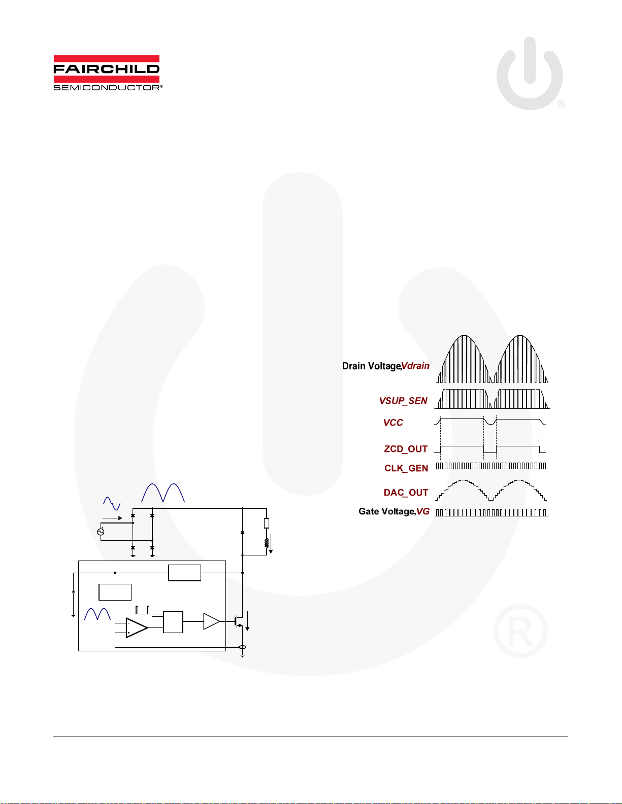
Figure 1. Basic Block of FL7701
The internal DAC_OUT reference signal is dependent on
the V
voltage. Using the DAC_OUT signal and internal
CC
clock, CLK_GEN; the FL7701 automatically makes a
digital reference signal, DAC_OUT. If the FL7701 cannot
detect the ZCD_OUT signal, the IC has an abnormal
internal reference signal. In this situation, this phenomenon
causes a lighting flicker.
Figure 2. FL7701 Operation
Soft-Start Function
The FL7701 has an internal soft-start to reduce inrush
current at IC startup. When the IC starts operation, the
internal reference of the IC slowly increases up to a fixed
level for around seven cycles. After settling down this
transient period, the internal reference is fixed at a certain
DC level. In this time, the IC continually tries to find input
phase information from the VCC pin. If the IC succeeds in
getting phase information from the VCC, the IC
automatically follows a similar shape reference, which it
made during the transient times, seven periods. If not, the
IC has a DC reference level.
© 2011 Fairchild Semiconductor Corporation www.fairchildsemi.com
Rev. 1.0.0 • 10/11/11
Page 2
AN-9744 APPLICATION NOTE
To precisely and reliably calculate the input voltage phase
on the VCC pin, the FL7701 uses a digital technique
(sigma/delta modulation/demodulation). After finishing this
digital technique, the FL7701 has new reference that is the
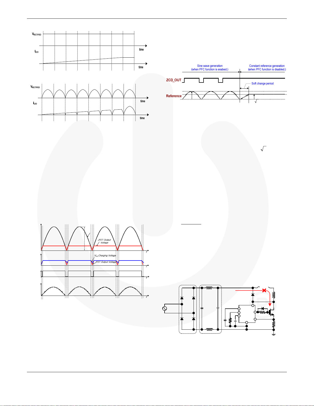
same phase as input voltage, as shown in Figure 6.
Figure 3. DC Input Condition
Figure 4. AC Input Condition
Internal Power Factor (PF) Function
The FL7701 application circuit does not use the input
electrolytic capacitor for voltage rectification after a bridge
diode because this system design results in a high pulse
shape input current. This pulse shape current contains many
harmonic components, so the total system cannot have high
PF. To get high PF performance, the FL7701 uses a
different approach.
The FL7701 has an intelligent internal PFC function that
does not require additional detection pins or other
components. The IC does not need a bulk capacitor on the
VCC pin for supply voltage stabilization.
V
bridge
Input Voltage
Peak
Bridge Diode
Output Voltage
Vp
/2Vp
Figure 6. Internal Reference
This signal enters the final comparator and current
information from the sensing resistor. Pin 1 is compared. As
a result, the FL7701 has a high power factor and can
operate as a normal peak current controller as shown in
Figure 6, in the DC input condition. The relationship
between AC Input Mode and DC Input Mode is
.
2
Output Frequency Programming
The FL7701 can program output frequency using an RT
resistor or with the RT pin in open condition. The FL7701
can have a fixed output frequency around 45kHz when the
RT pin is left open. For increasing system reliability, a
small-value capacitor is recommended below 100nF in RTopen condition. The relationship between output frequency
and the RT resistor is:
9
1002.2
f
OSC
[Hz]
RT
(1)
Output Open-Circuit Protection
VCC
The recommended connection method is shown in Figure 7.
The FL7701 has a high-voltage power supply circuit, which
self biases using high-voltage process device. If the LED
ZCD
DAC_OUT
Figure 5. Internal PFC Function
The FL7701 detects the VCC changing point for making the
Zero Crossing Detection (ZCD) signal, which is an internal
timing signal for making DAC_OUT. Normally, a capacitor
does not connect to the chip, the IC cannot start.
BD
EMI filter
L1
C1
L2
C2
ADIM
RT
VCC
R3
C3
C4
D1
HV
FL7701
GND
OUT
LED
L
D2
R1
CS
R2
connected to the VCC pin is used for voltage stabilization
and acts as low-pass filter or noise-canceling filter. This
increases the ability to get a stable timing signal at the VCC
Figure 7. LED Open Condition
pin, even is there may be noise on other pins.
© 2011 Fairchild Semiconductor Corporation www.fairchildsemi.com
Rev. 1.0.0 • 10/11/11 2
Page 3
AN-9744 APPLICATION NOTE
Inductor Short-Circuit Protection
The FL7701 has an Abnormal Over-Current Protection
(AOCP) function. If the voltage of the LED current-sensing
resistor is higher than 2.5V, even within Leading EdgeBlanking (LEB) time of 350ns; the IC stops operation.
VCC
RT OUT
GND
VCC
ZCD
Oscillator
time
ZCD
DAC
Soft start
Digital Block
Reference
UVLO
TSD
-
+
LEB
Leading Edge
Blanking
JFET
S
Q
R
-
+
AOCP
2.5V
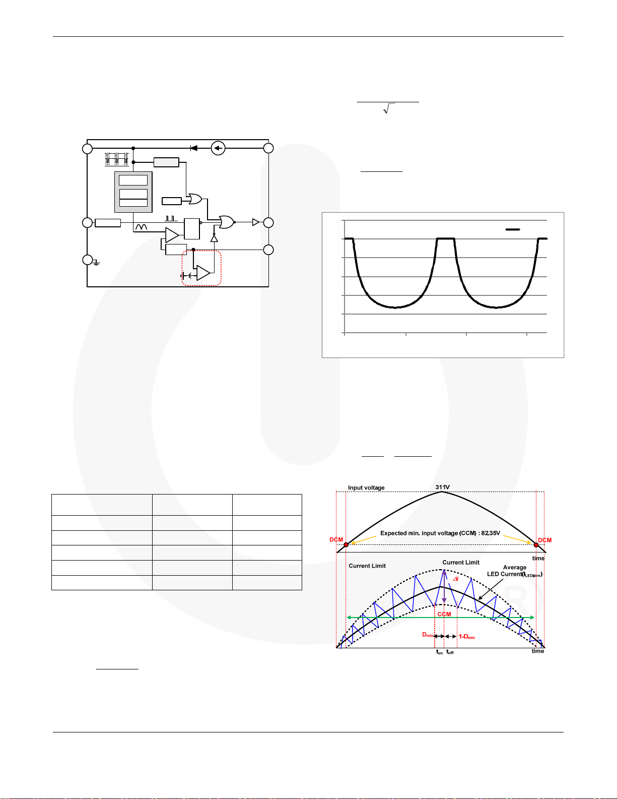
Figure 8. AOCP Function
HV
CS
Analog Dimming Function
The Analog Dimming (ADIM) function adjusts the output
LED current by changing the voltage level of the ADIM pin.
Application Information
The FL7701 is an innovative buck converter control IC
designed for LED applications. It can operate from DC and
AC input voltages without limitation and its input voltage
level can be up to 305V
Table 1 shows one example of a design target using the
FL7701 device.
or 400VDC.
AC
For example, if V
= 220V and ten LEDs are in series
IN(max)
connection, the minimum duty ratio is:
5.310
D
min
220285.0
132.0
Step 2: Maximum Duty Ratio
Similar to Step 1, calculate maximum duty ratio as:
nV
D
max
F
V
in
(min)
(3)
60
[%]
50
40
30
20
10
0
051015
Duty
[ms]
Figure 9. Duty Variation vs. Time
The FL7701 has a 50% maximum duty cycle to prevent
sub-harmonic instability. Assume the minimum input
voltage enters 50% duty ratio. Using Equation 2, recalculate the minimum input voltage for CCM operation:
nV
F
V
in
(min)
D
35
5.085.0
][35.82
V
(4)
Table 1. Target Design Specification
Item Specification Note
Frequency 45kHz
Output Voltage 35 VF=3.5V,
Output LED Current 0.3 rms
Output LED Current 0.5 Peak
Input Voltage (Max.) 220 V
AC(rms)
Step 1: Minimum Duty Ratio
The FL7701 has a fixed internal duty ratio range between
2% and 50%. This range depends on the input voltage and
the number of LEDs in the string.
nV
F
D
min
V
(max)
in
(2)
Figure 10. Estimated Waveforms
where η is efficiency of system; V
input voltage; V
is forward-drop voltage of LED; and n
F
is maximum
IN(max)
is LED number in series connection.
© 2011 Fairchild Semiconductor Corporation www.fairchildsemi.com
Rev. 1.0.0 • 10/11/11 3
Page 4

AN-9744 APPLICATION NOTE
Step 3: Maximum On/Off Time
The FL7701 has internally fixed maximum duty ratio
around 0.5 to prevent sub-harmonic instability. Assume the
maximum on/off time. For example, the maximum on/off
time at 45kHz operation condition is:
s
1
90000
[μs]
11.11
1
tt
offon
f
2
Step 4: Calculate the LED Current Ripple, ∆I
The Figure 11 shows the typical LED current waveforms of
a FL7701 application. For more stable or linear LED current,
operate in CCM.
In Equation 10, the desired average LED current is always
located between LED peak value, 500mA, which is limited
by the IC itself, and the LED minimum current. Using this
characteristic, the inductor value for the desired output
current ripple range (∆I) is:
V
(
IN
(max)
L 22.5
Figure 12. Current Ripple (∆I) vs. Inductance
min
DD
)
1)(
min
Isf
)132.01(132.02202
1516.045000
mH
Therefore, the minimum current is 0.19A.
Figure 11. Target Waveforms of LED Current
Using the typical LED current waveform in Figure 11,
derive the formula as:
I
I
II
aveLEDpk
or
)(
2
II
)(min
aveLED
2
(5)
The LED ripple current is defined as:
or
)2(2
where I
LED(AVE)
III
)(aveLEDpk
is equal to I
LEDrms
aveLED
.
)2(2
III
min)(
(6)
From the Table 1, the target average LED current is defined
as 0.3A and the LED peak current is set to 0.5A,. To
calculate the LED current ripple:
III
)(
aveLEDpk
[A]
1516.0)4242.05.0(2)2(2
Step 5: Inductance
Derive one more formula for the minimum inductance value
of the inductor using the Step 4 results:
DDV
)1)((
in
L
s
minmin(max)
If
(7)
Figure 13. Expected Waveforms
As a result, assume the expected output and input power:
[W]
P
INPUT
IVP
aveLEDLEDLED
P
LED
94.11
[W]
15.10)(
Step 6: Sensing Resistor
The FL7701 pulse-by-pulse current-limit of OSV protects
the IC and the whole system. Calculate the sensing resistor
value as:
5.0
[]
1
R
I
pk
(8)
The power rating is under 0.25W even when considering
power consumption at peak-current condition.
© 2011 Fairchild Semiconductor Corporation www.fairchildsemi.com
Rev. 1.0.0 • 10/11/11 4
Page 5

AN-9744 APPLICATION NOTE
N
Step 7: Calculate Energy-Handing Capability (w-s):
Energy
LI
2
pk
2
2
23
)5.0)(1066.4(
000583.0
[w-s]
(9)
Step 8: Calculate Electrical Conditions, Ke
For example, if 10eas, 1W LED for making 12.2W output
power (V
=3.5V, I
F
=0.35A), set up equation as:
LED(rms)
42
10145.0
BPK
moe
42
0000283.0104.02.12145.0
where Po is target output power and Bm is operating
flux density [T].
Step 9: Calculate Regulation Inductor α.
The regulation can be expressed as the power loss on the
copper at inductor:
P
copperloss
P
o
[%]
100@
(10)
Assume the regulation, α, is assigned in Step 1 because
system loss is strongly related to system efficiency.
@
PPP
oincopperloss
(11)
[W]
55.1)1()1(
So, calculate the regulation as:
P
copperloss
@
P
o
100
55.1
2.12
%7.12100
(12)
In this design, 10% was used instead of 12.7% because
there is another power consumption factor on this
application, P
FRD
or P
switching
.
Step 10: Calculate Core Geometry, Kg
Calculate the core geometry:
Energy
K
g
K
e
22
000583.0)(
000012.0
100000283.0
[cm5]
(13)
Step 11: Select a Core
Select a core comparable in core geometry Kg, using core
information on the core maker’s site (see Table 2).
Table 2. Available Core Information
Part No. MLT[cm] Ac[cm2] Wa[cm2] Ap[cm4] Kg[cm5]
EFD-10
EPC-40506
EE-40904
(Mag)
EE0908S
(Samhwa)
EE-41205
(Mag)
EE1312S
(Samhwa)
1.82 0.0650 0.1163 0.007556 0.000108
1.085 0.0410 0.0198 0.0008131 0.000123
1.664 0.036 0.064 0.002304 0.000020
0.0253 0.0253 0.0027
0.202 0.148 0.03
0.153 0.349 0.0253
Notes:
1. Mag(magnetic): www.mag-inc.com
2. Samhwa: www.samwha.co.kr/electronics/
According to Table 2, select a core larger than EEFD-10 to
overcome core saturation. Among core types, the EE core is
the most popular because of its common shape and low cost.
Select the EE core for this design.
Figure 14. Minimum Available Core Size
(EE-40904(Mag))
Step 12: Calculate the Number of Turns, N
Select core turns if there is a well-known AL value
estimated for certain turn conditions without gap condition:
N
L
[T] or
AL
AL
L
2
(14)
To add a gap between cores to prevent core saturation, find
a real AL-value using certain gap conditions. Select one of
possible cores from Table 2; but it should have a larger Kg
value than calculation results from Step 11. In this design
step, EE1312S core was used because this part is available
in the open market. Applying the EE1312S with gap made
by three-layer insulation tape, 8.3µH measured when ten
turns are winded the core. So, calculate a new AL-value
with three-layer insulation tape as:
AL
new
L
2
N
6
1083.0
Using the new AL value, calculate the needed turns for
the inductor:
3
1066.4
L
N
AL
6
1083.0
[T]
92.74
In this design, 75T was used.
Step 13: Calculate the Current Density
Calculate the current density, J, using a window utilization
=0.4:
k
U
NI
J
)(
rmsAVELED
KW
ua
Step 14: Calculate Required Bare Wire Area, A
I
)(
A
)(
Bw
rmsAVELED
J
29.075
29.0
4.00253.0
000134.0
20.2149
20.2149
[cm2]
W(B):
© 2011 Fairchild Semiconductor Corporation www.fairchildsemi.com
Rev. 1.0.0 • 10/11/11 5
Page 6

AN-9744 APPLICATION NOTE
Step 15: Calculate Skin Depth, γ
The skin depth is the radius of the wire:
62.6
f
s
[cm]
031.0
Step 16: Calculate the Wire Area:
2
A
rwire
[cm2]
0030.0031.014.3
Step 17: Select a Wire
Comparing Step 14 and Step 16 results. If the result of Step
17 is larger than the result of Step 14, need wire strands are
not needed.
Step 18: Select Wire Size
Select the wire size with required area Table 3. AWG 35
with single wire in this case.
Table 3. Wire Table AWG
Bare Wire
Area [cm
34 0.00002011 0.0002863 0.16
35 0.0001589 0.0002268 0.14
36 0.0001266 0.001813 0.127
2
]
Heavy
Insulation [cm2]
Diameter [mm]
Table 4. Design Results
Selected Core EE1312S
Turns 75
Gap 3 Layers
Wire AWG35/0.14mm
© 2011 Fairchild Semiconductor Corporation www.fairchildsemi.com
Rev. 1.0.0 • 10/11/11 6
Page 7

AN-9744 APPLICATION NOTE
System Verification
Figure 15 shows the recommended circuit of a FL7701
system with just a few components.
Figure 15. Test Circuit
Figure 16 and Figure 17 show the startup waveforms from a
on FL7701 application in DC and AC input conditions at
220V with ten LEDs.
VCC[5V/div]
V
[100V/div]
DRAIN
I
[0.2A/div]
LED
Figure 18 and Figure 19 show performance of FL7701
following the input source changes from high-line
frequency, to lower frequency, then to higher frequency.
V
[100V/div]
DRAIN
I
[0.2A/div]
LED
Figure 18. Input Source Changing: 45Hz to 100Hz
V
[100V/div]
DRAIN
Figure 16. Soft-Start Performance in DC
Input Condition
VCC[5V/div]
V
[100V/div]
DRAIN
I
[0.2A/div]
LED
Figure 17. Soft-Start Performance in AC
Input Condition
I
[0.2A/div]
LED
Figure 19. Input Source Changing: 100Hz to 45Hz
The Figure 20 shows the analog dimming performance with
changing V
. The output LED current changes according
ADIM
to the control voltage.
Figure 20. V
vs. LED Current
ADMIN
© 2011 Fairchild Semiconductor Corporation www.fairchildsemi.com
Rev. 1.0.0 • 10/11/11 7
Page 8

AN-9744 APPLICATION NOTE
Figure 21 shows the typical function of AOCP performance.
The FL7701 limits output LED current pulse-by-pulse with
Design Tips
Leading-Edge Blanking (LEB), ignoring current noise.
Even though the IC limits the output LED current pulse-by-
LED Current Changing
pulse, it cannot prevent inrush current during an inductor
short. To prevent this kind of abnormal situation, the IC has
an AOCP function to protect the system.
Figure 23 shows the recommended circuit for achieving
high PF. In this condition, the LED current goes to 0 every
half cycle period.
VCC[10V/div]
VDC[40V/div]
VCS[1V/div]
V
[7V/div]
GATE
Figure 21. AOCP Function
Figure 22 shows the typical waveforms of FL7701 system.
The LED current has the same phase as the input voltage
source and rectified sinusoidal waveform.
VDD[3V/div]
I
[0.1A/div]
LED
V
[100V/div]
DRAIN
To design around this, add an electrolytic capacitor in
parallel to the LED load, as shown in Figure 24. This added
capacitor provides a truer DC LED current.
VDD[3V/div]
I
[0.2A/div]V
LED
V
R
DRAIN
[100V/div
D
Figure 23. Typical Waveform
Figure 24. Circuit with Electrolytic Capacitor
Figure 22. Typical Operating Waveforms
VDD[3V/div]
[7V/div]
V
gate
I
[0.2A/div]
LED
V
[100V/div]
DRAIN
Figure 25. Typical with Bulk Capacitor
© 2011 Fairchild Semiconductor Corporation www.fairchildsemi.com
Rev. 1.0.0 • 10/11/11 8
Page 9
AN-9744 APPLICATION NOTE
Increasing System Reliability
To increase system reliability in noisy conditions, add a small
capacitor with below 100pF to the RT and ADIM pins. In
normal conditions, these components are unnecessary.
PCB Layout Guidelines
The PCB layout is important because a common application
would be to retrofit a lamp application, which requires a
small product size. The IC could be affected by noise, so
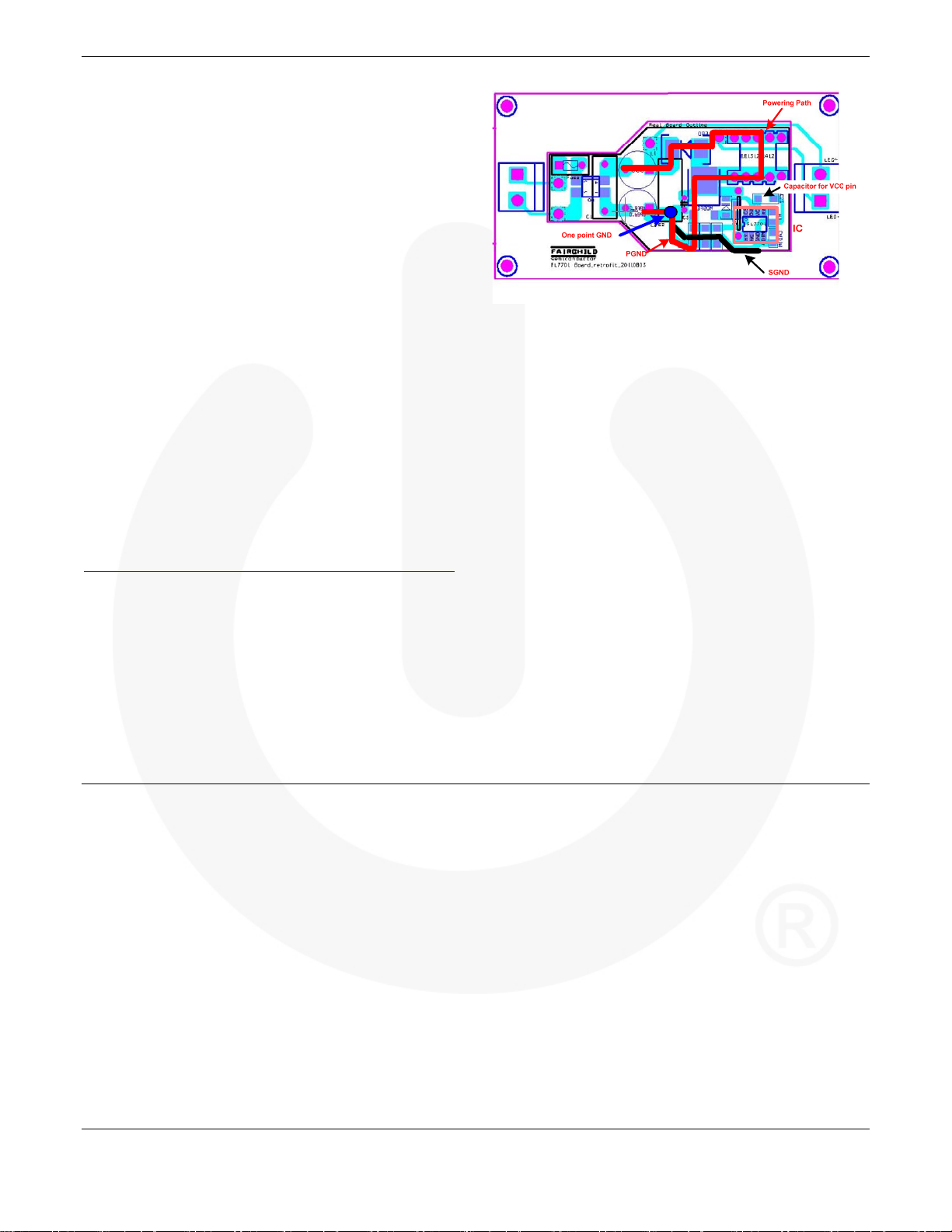
carefully follow the PCB layout guide lines:
Locate the IC on the external powering path.
Separate power GND and signal GND.
capacitor should be located close to the VCC pin.
V
CC
Figure 26. Example LED Layout
Related Datasheets
FL7701 — Smart LED Lamp Driver IC with PFC Function
DISCLAIMER
FAIRCHILD SEMICONDUCTOR RESERVES THE RIGHT TO MAKE CHANGES WITHOUT FURTHER NOTICE TO ANY PRODUCTS
HEREIN TO IMPROVE RELIABILITY, FUNCTION, OR DESIGN. FAIRCHILD DOES NOT ASSUME ANY LIABILITY ARISING OUT OF THE
APPLICATION OR USE OF ANY PRODUCT OR CIRCUIT DESCRIBED HEREIN; NEITHER DOES IT CONVEY ANY LICENSE UNDER ITS
PATENT RIGHTS, NOR THE RIGHTS OF OTHERS.
LIFE SUPPORT POLICY
FAIRCHILD’S PRODUCTS ARE NOT AUTHORIZED FOR USE AS CRITICAL COMPONENTS IN LIFE SUPPORT DEVICES OR SYSTEMS
WITHOUT THE EXPRESS WRITTEN APPROVAL OF THE PRESIDENT OF FAIRCHILD SEMICONDUCTOR CORPORATION.
As used herein:
1. Life support devices or systems are devices or systems which,
(a) are intended for surgical implant into the body, or (b)
support or sustain life, or (c) whose failure to perform when
properly used in accordance with instructions for use provided
in the labeling, can be reasonably expected to result in
significant injury to the user.
© 2011 Fairchild Semiconductor Corporation www.fairchildsemi.com
Rev. 1.0.0 • 10/11/11 9
2. A critical component is any component of a life support device
or system whose failure to perform can be reasonably expected
to cause the failure of the life support device or system, or to
affect its safety or effectiveness.
 Loading...