

Page 1
FAN7601B
Green Current Mode PWM Controller
FAN7601B — Green Current Mode PWM Controller
May 2012
Features
Green Current Mode PWM Control
Low Operating Current: Maximum 4mA
Burst Mode Operation
Internal High-Voltage Startup Switch
Under-Voltage Lockout (UVLO): 12V/8V
Latch Protection and Soft-Start Function
Over-Voltage Protection: 19V
Operating Frequency up to 300kHz
Maximum Duty Cycle: 95%
Applications
Offline Adapter Applications
Auxiliary Power Supplies
Related Resources
AN4129 — Green Current Mode PWM
Controller FAN7601
Description
The FAN7601B is a programmable frequency green
current mode PWM controller. It is specially designed for
the offline adapter applications and the auxiliary power
supplies that require high efficiency at light load and no
load. The internal high-voltage startup switch and burst
mode reduce the power loss.
FAN7601B includes protections, such as latch protection
and over-voltage protection. The latch protection can be
used for over-voltage protection, thermal protection, and
others. The soft-start prevents the output voltage
overshoot at startup.
Ordering Information
Operating
Part Number
FAN7601BM
FAN7601BMX 7601B 8-SOP Tape & Reel
FAN7601BGX 7601B 10-SSOP Tape & Reel
© 2008 Fairchild Semiconductor Corporation www.fairchildsemi.com
FAN7601B • Rev. 1.0.3
Junction
Temperature
-40°C to +150°C
Top Mark Package Packing Method
7601B 8-SOP Rail
Page 2
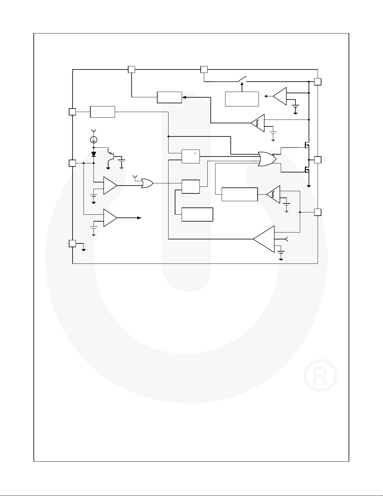
Block Diagram
R
t/Ct
(5)
V
REF
Latch/SS
(4)
3
OSC4
12µA
2.5V
FAN7601B — Green Current Mode PWM Controller
V
(10)
REF
5V Ref
1.5V
OVP
+
−
Enable
S
R
S
R
V
(1)
STR
18
V
CC
7
OVP
Startup
Circuit
UVLO
+
−
Q
Q
Delay
Circuit
+
−
12V/8V
+
−
19V
(8)
OUT
6
(7)
+
−
1V
GND
5
(6)
Note:
1. ( ) is 10-SSOP Pin Number.
Startup
Circuit
Reset
Circuit
Figure 1. Internal Block Diagram
0.97V/0.9V
+
−
Latch/SS
−
1V
2
CS/FB
(3)
© 2008 Fairchild Semiconductor Corporation www.fairchildsemi.com
FAN7601B • Rev.1.0.3 2
Page 3
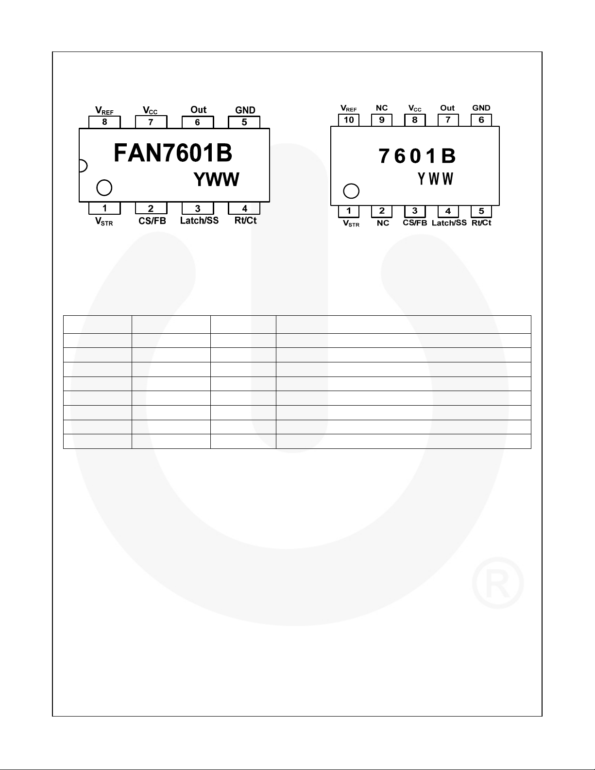
Pin Configurations
FAN7601B — Green Current Mode PWM Controller
Figure 2. 8-Pin Configuration (Top View) Figure 3. 10-Pin Configuration (Top View)
Pin Definitions
Pin # (8-Pin) Pin # (10-Pin) Name Description
1 1 V
2 3 CS/FB Current Sense and Feedback
3 4 Latch/SS Latch Protection and Soft-Start
4 5 Rt/Ct Oscillator Timing
5 6 GND Ground
6 7 Out Gate Drive Output
7 8 VCC IC Power Supply
8 10 V
Startup
STR
Voltage Reference
REF
© 2008 Fairchild Semiconductor Corporation www.fairchildsemi.com
FAN7601B • Rev.1.0.3 3
Page 4

Absolute Maximum Ratings
Stresses exceeding the absolute maximum ratings may damage the device. The device may not function or be
operable above the recommended operating conditions and stressing the parts to these levels is not recommended. In
addition, extended exposure to stresses above the recommended operating conditions may affect device reliability. The
absolute maximum ratings are stress ratings only.
Symbol Parameter Min. Max. Unit
VCC Supply Voltage 20 V
V
Input Voltage CS/FB -0.3 20.0 V
CS/FB
T
Storage Temperature -55 +150
STG
TJ Recommended Operating Junction Temperature -40 +150
IO Output Current 250 mA
V
STR
ESD
V
Input Voltage 500 V
STR
Electrostatic Discharge
Capability
Human Body Model, JESD22-A114 2000
Charged Device Model, JESD22-C101 1500
°C
°C
V
Thermal Impedance
FAN7601B — Green Current Mode PWM Controller
Symbol Parameter Value Unit
θ
JA
Thermal Resistance, Junction-to-Ambient
8-SOP 180
10-SSOP 130
°C/W
© 2008 Fairchild Semiconductor Corporation www.fairchildsemi.com
FAN7601B • Rev.1.0.3 4
Page 5

Electrical Characteristics
TA=-25°C~125°C, VCC=14V, RT=9.5kΩ, CT=2.2nF unless otherwise specified.
Symbol Parameter Conditions Min. Typ. Max. Unit
Reference Section
V
REF
ΔV
REF1
ΔV
REF2
Oscillator Section
f
OSC
ST
V
OSC
PWM Section
V
CS/FB1
D
MAX
D
MIN
Burst Mode Section
V
CS/FB2
V
CS/FB3
Soft-Start Section
ISS Soft-Start Current V
VSL Soft-Start Limit Voltage
Protection Section
V
LATCH
V
OVP
UVLO Section
V
tH
V
tL
Total Current Section
IOP Operating Supply Current 3 4 mA
Output Section
VOL Low Output Voltage
VOH High Output Voltage
tr Rising Time
tf Falling Time
Startup Section
Reference Output Voltage IO=1mA
Line Regulation VCC=10V~18V
Load Regulation IO=1mA ~ 10mA
4.85 5.00 5.15 V
10 20 mV
20 30 mV
Initial Accuracy 90 100 110 kHz
Voltage Stability VCC=10V~18V
V
Amplitude V
pin4 peak-to-peak
1.0 1.5 %
1.25 V
CS/FB Threshold Voltage1 0.9 1.0 1.1 V
Maximum Duty Cycle TA=25°C 92 95 98 %
Minimum Duty Cycle 0 %
CS/FB Threshold Voltage2
CS/FB Threshold Voltage3
(2)
0.77 0.97 1.17 V
(2)
0.7 0.9 1.1 V
=GND 9 12 15
(3)
pin3
ISS=1μA
1.2 1.5 1.8 V
Latch Voltage 2.25 2.50 2.75 V
Over-Voltage Protection 18 19 20 V
Start Threshold Voltage 11 12 13 V
Minimum Operating Voltage 7 8 9 V
=25°C, IO=100mA
T
A
T
=25°C, IO=-100mA
(2)
(2)
A
TA=25°C, CI=1nF
TA=25°C, CI=1nF
2.0 2.5 V
11.5 12.0 14.0 V
45 150 ns
35 150 ns
μA
FAN7601B — Green Current Mode PWM Controller
I
V
str
Startup Current V
STR
=30V, TA=25°C 0.5 1.0 1.5 mA
STR
Notes:
2. These parameters, although guaranteed, are not 100% tested in production.
3. It is recommended to connect a 1MΩ resistor between the Latch/SS pin and GND to prevent abnormal operation of
the latch protection by noise coupling.
© 2008 Fairchild Semiconductor Corporation www.fairchildsemi.com
FAN7601B • Rev.1.0.3 5
Page 6

Typical Performance Characteristics
c
5.05
5.03
5.01
(V)
Vref
4.99
4.97
4.95
-45 -25 -15 0 25 50 80 100 125 140
Junction Temperature(℃)
Figure 4. Trimmed Reference Voltage Figure 5. Supply Current
13
12.5
12
11.5
(V)
11
10.5
Vcc Star t Thresh old VtH
10
-45 -25 -15 0 25 50 80 100 125 140
Junction Temperature(℃)
Figure 6. VCC Start Threshold Voltage Figure 7. VCC Stop Threshold Voltage
FAN7601B — Green Current Mode PWM Controller
3
2.5
2
1.5
(mA)
1
Supply Current Icc
0.5
0
-45 -25 -15 0 25 50 80 100 125 140
Junction Temperature(℃)
9
8.5
8
(V)
7.5
Vcc Stop Threshold VtL
7
-45 -25 -15 0 25 50 80 100 125 140
Junction Temperature(℃)
110
105
100
95
(KHz)
90
Oscillator Frequency Fos
85
-45 -25 -15 0 25 50 80 100 125 140
Junction Temperature(℃)
100
98
96
94
(%)
92
90
Maximum Duty Cycle Dmax
-45 -25 -15 0 25 50 80 100 125 140
Junction Temperature(℃)
Figure 8. Oscillator Frequency Figure 9. Maximum Duty Cycle
2.7
2.6
2.5
(V)
2.4
2.3
Oscillator High Threshold VrH
-45 -25 -15 0 25 50 80 100 125 140
Junction Temperature(℃)
1.35
1.3
1.25
(V)
1.2
1.15
Oscillator Low Threshold VrL
-45 -25 -15 0 25 50 80 100 125 140
Junction Temperature(℃)
Figure 10. Oscillator High Threshold Voltage Figure 11. Oscillator Low Threshold Voltage
© 2008 Fairchild Semiconductor Corporation www.fairchildsemi.com
FAN7601B • Rev.1.0.3 6
Page 7

p
h
f
]
Typical Performance Characteristics (Continued)
FAN7601B — Green Current Mode PWM Controller
2
1.6
1.2
0.8
(mA)
0.4
Start up Current Istr
0
-45 -25 -15 0 25 50 80 100 125 140
Junction Temperature(℃)
Figure 12. Startup Current
2.8
2.7
2.6
2.5
(V)
2.4
2.3
Latch Protection Vlatc
2.2
-45 -25 -15 0 25 50 80 100 125 140
Juncti on Temperatu re(℃)
Figure 14. Latch Protection Voltage
20
19.6
19.2
(V)
18.8
18.4
18
Over Voltage Prot ection Vov
-45 -25 -15 0 25 50 80 100 125 140
Junctio n Temperature( ℃)
Figure 13. Over-Voltage Protection Level
14
13
12
11
(uA)
10
Soft Start Current Iso
9
-45 -25 -15 0 25 50 80 100 125 140
Junction Temperature(℃)
Figure 15. Soft-Start Current
1000
Ct=
10nF
100
Frequency[KHz
10
1
5K 15K 25K 35K 45K
Rt[Kohm]
8.2nF
4.7nF
3.3nF
2.2nF
1nF
820pF
680pF
Figure 16. Oscillator Frequency Characteristic
© 2008 Fairchild Semiconductor Corporation www.fairchildsemi.com
FAN7601B • Rev.1.0.3 7
Page 8

Physical Dimensions
8
5.00
4.80
3.81
FAN7601B — Green Current Mode PWM Controller
A
0.65
5
B
6.20
5.80
4.00
1.75
5.60
3.80
PIN ONE
INDICATOR
(0.33)
1
0.25
1.27
4
1.27
CMBA0.25
LAND PATTERN RECOMMENDATION
SEE DETAIL A
0.10
0.25
1.75 MAX
0.51
0.33
0.50
R0.10
0.25
R0.10
8°
0°
0.90
0.406
Package drawings are provided as a service to customers considering Fairchild components. Drawings may change in any manner
without notice. Please note the revision and/or date on the drawing and contact a Fairchild Semiconductor representative to verify or
obtain the most recent revision. Package specifications do not expand the terms of Fairchild’s worldwide terms and conditions, specifically the
warranty therein, which covers Fairchild products.
Always visit Fairchild Semiconductor’s online packaging area for the most recent package drawings:
http://www.fairchildsemi.com/packaging/
(1.04)
DETAIL A
SCALE: 2:1
Figure 17. 8-Lead, Small Outline Package (SOP)
.
C
0.10 C
x 45°
GAGE PLANE
0.36
SEATING PLANE
0.19
OPTION A - BEVEL EDGE
OPTION B - NO BEVEL EDGE
NOTES: UNLESS OTHERWISE SPECIFIED
A) THIS PACKAGE CONFORMS TO JEDEC
MS-012, VARIATION AA, ISSUE C,
B) ALL DIMENSIONS ARE IN MILLIMETERS.
C) DIMENSIONS DO N OT INCLUDE MOLD
FLASH OR BURRS.
D) LANDPATTERN STANDARD: SOIC127P600X175-8M.
E) DRAWING FILENAME: M08AREV13
© 2008 Fairchild Semiconductor Corporation www.fairchildsemi.com
FAN7601B • Rev.1.0.3 8
Page 9

Physical Dimensions
5.12
4.72
4.00
FAN7601B — Green Current Mode PWM Controller
0.65
6 10
1.75
6.30
5.70
PIN ONE
INDICATOR
#1
TOP VIEW
5
(1.00)
4.15
3.75
1.80 MAX
0.25
0.10
0.506
0.306
(0.26)
SIDE VIEW END VIEW
NOTES:
A) NO DRAWING STANDARD APPLIES TO THIS PACKAGE
B) ALL DIMENSIONS ARE IN MILLIMETERS.
C) DIMENSIONS ARE EXCLUSIVE OF BURRS, MOLD FLASH,
AND TIE BAR EXTRUSIONS.
D) LAND PATTERN RECOMMENDATION IS FSC SOURCED.
E) DRAWING FILE NAME AND REVISION : MKT-MSB10A,REV1
R0.15
0.70
0.30
#1
(1.00)
LAND PATTERN RECOMMENDATION
SEE DETAIL A
R0.15
8¡Æ
(2.04)
5.60
R0.20
0.30
0.15
GAGE PLANE
(0.36)
SEATING PLANE
DETAIL A
SCALE: 2:1
Figure 18. 10-Lead, Small Outline Package (SSOP)
Package drawings are provided as a service to customers considering Fairchild components. Drawings may change in any manner
without notice. Please note the revision and/or date on the drawing and contact a Fairchild Semiconductor representative to verify or
obtain the most recent revision. Package specifications do not expand the terms of Fairchild’s worldwide terms and conditions, specifically the
warranty therein, which covers Fairchild products.
Always visit Fairchild Semiconductor’s online packaging area for the most recent package drawings:
http://www.fairchildsemi.com/packaging/
© 2008 Fairchild Semiconductor Corporation www.fairchildsemi.com
FAN7601B • Rev.1.0.3 9
.
Page 10

FAN7601B — Green Current Mode PWM Controller
© 2008 Fairchild Semiconductor Corporation www.fairchildsemi.com
FAN7601B • Rev.1.0.3 10
 Loading...