

Page 1

www.fairchildsemi.com
FEB388_003
FAN9611/FAN9612 400W Interleaved
Dual BCM PFC Controller
Evaluation Board User Guide
Featured Fairchild Product: FAN9611, FAN9612
Please contact a local Fairchild Sales representative
for an evaluation board.
© 2010 Fairchild Semiconductor Corporation 1 FEB388_FAN9611/12 • Rev. 0.0.3
Page 2

www.fairchildsemi.com
Table of Contents
1. Overview of the Evaluation Board ........................................................................................... 3
2. Key Features ............................................................................................................................. 4
3. Specifications ............................................................................................................................ 5
4. Test Procedure .......................................................................................................................... 6
5. Schematic .................................................................................................................................. 7
6. Boost Inductor Specification .................................................................................................... 8
7. Line Filter Inductor Specifications ........................................................................................... 9
8. PCB Layout ............................................................................................................................. 10
9. Bill of Materials (BOM) ......................................................................................................... 14
10.Test Results ............................................................................................................................. 16
10.1. Startup ......................................................................................................................... 16
10.2. Normal Operation ....................................................................................................... 18
10.3. Line Transient ............................................................................................................. 20
10.4. Load Transient ............................................................................................................ 21
10.5. Brownout Protection ................................................................................................... 22
10.6. Phase Management ..................................................................................................... 24
10.7. Efficiency .................................................................................................................... 27
10.8. Harmonic Distortion and Power Factor ...................................................................... 28
11.References ............................................................................................................................... 30
12.Ordering Information .............................................................................................................. 30
13.Revision History ..................................................................................................................... 30
© 2010 Fairchild Semiconductor Corporation 2 FEB279_FAN9611/12 • Rev. 0.0.3
Page 3

www.fairchildsemi.com
The following user guide supports the FAN9611/12 400W evaluation board for
interleaved boundary-conduction-mode power-factor-corrected supply. It should be used
in conjunction with the FAN9611/12 datasheet as well as the Fairchild application note
AN-6086 Design Considerations for Interleaved Boundary-Conduction Mode PFC Using
FAN9611 / FAN9612. Although marked FAN9612, the evaluation board can be
interchangeably used to evaluate either the FAN9611 (10V turn-on threshold) or
FAN9612 controller (12.5V turn-on threshold). Please visit Fairchild’s website at
www.fairchildsemi.com
for additional information.
1. Overview of the Evaluation Board
The FAN9611/12 interleaved dual Boundary-Conduction-Mode (BCM) Power-FactorCorrection (PFC) controllers operate two parallel-connected boost power trains 180º out
of phase. Interleaving extends the maximum practical power level of the control
technique from about 300W to greater than 800W. Unlike the continuous conduction
mode (CCM) technique often used at higher power levels, BCM offers inherent zerocurrent switching of the boost diodes (no reverse-recovery losses), which permits the use
of less expensive diodes without sacrificing efficiency. Furthermore, the input and output
filters can be smaller due to ripple current cancellation between the power trains and
doubling of effective switching frequency.
The advanced line feedforward with peak detection circuit minimizes the output voltage
variation during line transients. To guarantee stable operation with less switching loss at
light load, the maximum switching frequency is clamped at 525kHz. Synchronization is
maintained under all operating conditions.
Protection functions include output over-voltage, over-current, open-feedback, undervoltage lockout, brownout, and redundant latching over-voltage protection. The
FAN9611/12 is available in a lead-free 16-lead SOIC package.
This FAN9611/12 evaluation board is a four-layer board designed for 400W (400V/1A)
rated power. Thanks to the phase management, the efficiency is maintained above 96% at
low-line and high-line, even down to 10% of the rated output power. Efficiency is 96.4%
at line voltage 115V
and 98.2% at 230V
AC
under full-load conditions.
AC
© 2010 Fairchild Semiconductor Corporation 3 FEB279_FAN9611/12 • Rev. 0.0.3
Page 4
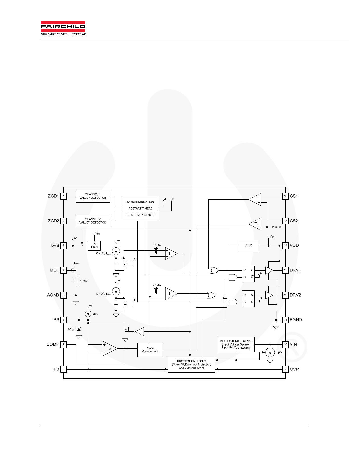
www.fairchildsemi.com
2. Key Features
Low Total Harmonic Distortion, High Power Factor
180° Out-of-Phase Synchronization
Automatic Phase Disable at Light Load
1.8A Sink, 1.0A Source, High-Current Gate Drivers
Transconductance (g
Voltage-Mode Control with (V
Closed-Loop Soft-Start with Programmable Soft-Start Time for Reduced Overshoot
Minimum Restart Timer Frequency to Avoid Audible Noise
Maximum Switching Frequency Clamp
Brownout Protection with Soft Recovery
Non-Latching OVP on FB Pin and Second-Level Latching Protection on OVP Pin
Open-Feedback Protection
Over-Current and Power-Limit Protection for Each Phase
Low Startup Current: 80µA Typical
Works with DC, 50Hz to 400Hz AC Inputs
) Error Amplifier for Reduced Overshoot
M
)2 Feed-forward
IN
Figure 1. Block Diagram
© 2010 Fairchild Semiconductor Corporation 4 FEB279_FAN9611/12 • Rev. 0.0.3
Page 5

www.fairchildsemi.com
3. Specifications
This board has been designed and optimized for the following conditions:
Input Voltage Range Rated Output Power
VIN Nominal : 85~264VAC
V
Supply : 13VDC~18VDC
DD
Note:
1. Minimum output voltage during the 20ms hold-up time is 330VDC.
400W 400V-1A
Output Voltage
(Rated Current)
V
V
f
Efficiency > 96% down to 20% load (115V
Efficiency > 97% down to 20% load (230V
= 85~264VAC
LINE
= 400V
OUT
> 50kHz
SW
AC
AC
)
)
PF > 0.99 at full load
The trip points for the built-in protections are set as below in the evaluation board.
The non-latching output OVP trip point is set at 108% of the nominal output voltage.
The latching output OVP trip point is set at 117% of the nominal output voltage.
The line UVLO (brownout protection) trip point is set at 68V
(10VAC hysteresis).
AC
The pulse-by-pulse current limit for each MOSFET is set at 9.1A.
The maximum power limit is set at ~120% of the rated output power. The phase
management function permits phase shedding/adding ~15% of the nominal output power
for high line (230V
). This level can be programmed by modifying MOT resistor (R6).
AC
© 2010 Fairchild Semiconductor Corporation 5 FEB279_FAN9611/12 • Rev. 0.0.3
Page 6
www.fairchildsemi.com
4. Test Procedure
Before testing the board; DC voltage supply for VDD, AC voltage supply for line input,
and DC electric load for output should be connected to the board properly.
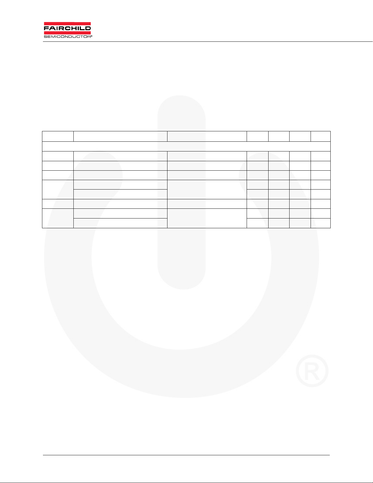
1. Supply V
specification for V
for the control chip first. It should be higher than 13V (refer to the
DD
turn-on threshold voltage in Table 1).
DD
Table 1. Specification Excerpt from FAN9611/12 Datasheet
Symbol Parameter Conditions Min. Typ. Max. Unit
Supply
I
Startup Supply Current VDD = VON – 0.2V 80 110 µA
STARTUP
IDD Operating Current Output Not Switching 3.7 5.2 mA
I
Dynamic Operating Current fSW = 50kHz; C
DD_DYM
VON
V
OFF
V
HYS
UVLO Start Threshold, FAN9611
UVLO Start Threshold, FAN9612 12.0 12.5 13.0 V
UVLO Stop Threshold Voltage VDD Decreasing 7.0 7.5 8.0 V
UVLO Hysteresis, FAN9611
UVLO Hysteresis, FAN9612 5.0
VDD Increasing
V
– V
OFF
ON
= 2nF 4 6 mA
LOAD
9.5 10.0 10.5 V
2.5
V
V
2. Connect the AC voltage (85~265VAC) to start the FAN9611/12 evaluation board.
Since FAN9611/12 has brownout protection, any input voltages lower than operation
range triggers the protection.
3. Change load current (0~1A) and check the operation.
© 2010 Fairchild Semiconductor Corporation 6 FEB279_FAN9611/12 • Rev. 0.0.3
Page 7
www.fairchildsemi.com
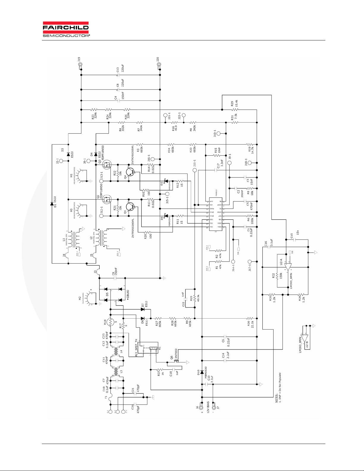
5. Schematic
Figure 2. FAN9611/12 400W Evaluation Board Schematic
© 2010 Fairchild Semiconductor Corporation 7 FEB388_FAN9611/12 • Rev. 0.0.3
Page 8
www.fairchildsemi.com
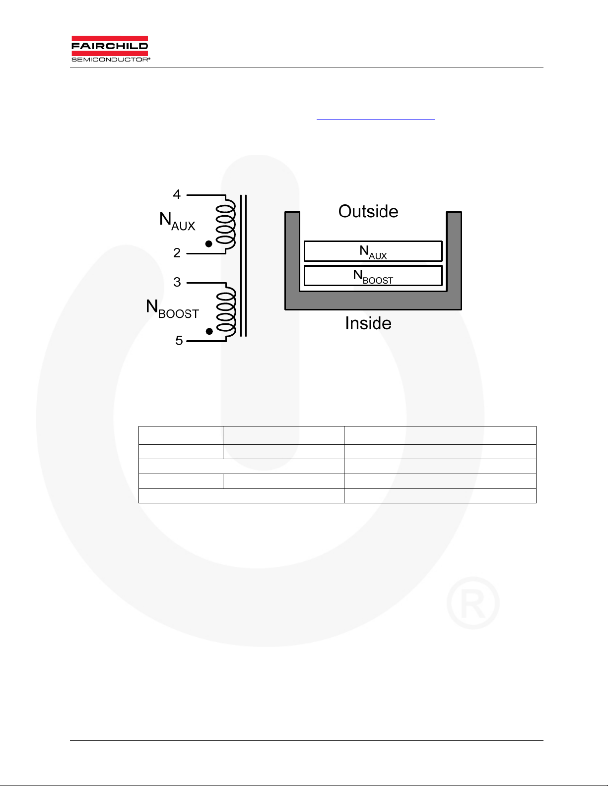
6. Boost Inductor Specification
PA2975NL-5P4 from Pulse Electronics (www.pulseelectronics.com)
Core: PQ3230 (Ae=161mm2)
Bobbin: PQ3230
Inductance : 200H
Figure 3. Boost Inductor used in this FAN9611/12 Evaluation Board
Table 2. Inductor Turns Specifications
Pin Turns
N1 5 3 30
Insulation Tape
N2 2 4 3
Insulation Tape
© 2010 Fairchild Semiconductor Corporation 8 FEB388_FAN9611/12 • Rev. 0.0.3
Page 9
www.fairchildsemi.com
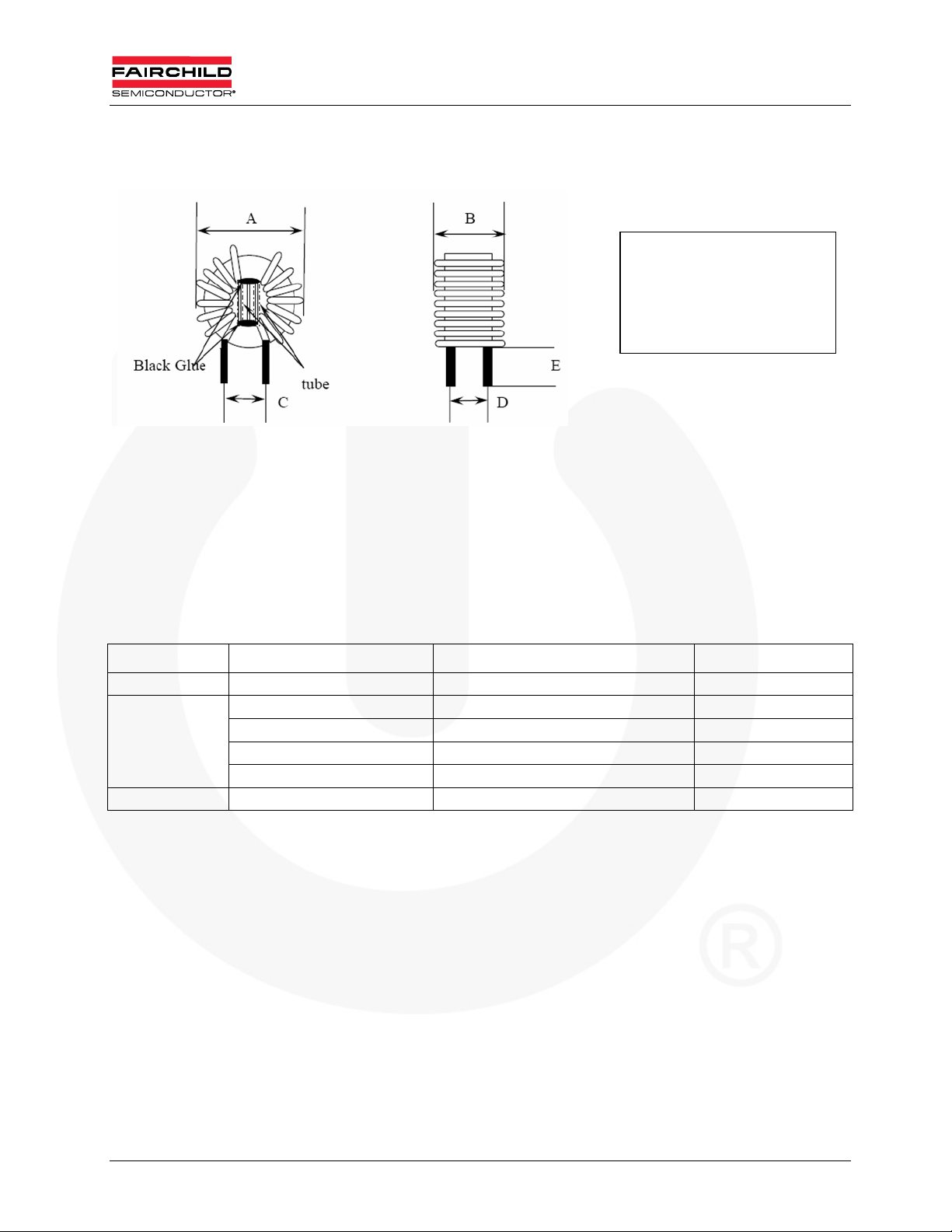
7. Line Filter Inductor Specifications
Electrical Specifications (1kHz, 1V)
- Inductance: 9.0mH (min.) for each winding
- DC resistance: 0.05Ω (max.) for each winding
- Number of turns: 0.9mm×2/30.5 turns for each winding
Figure 4. Line Filter Inductor Specification
A : 30mm (max)
B: 15 mm (max)
C: 11 mm
D: 13 mm
E: 15±1 mm
Table 3. Materials List
Component Material Manufacturer UL File Number
Core T22x14x08 Core T22x14x08, TOMITA
THFN-216 Ta Ya Electric Wire Co,. Ltd. E197768
Wire
Solder 96.5%, Sn, 3%, Ag, 0.5% Cu Xin Yuan Co., Ltd.
UEWN/U PACIFIC Wire and cable Co., Ltd. E201757
UEWE Tai-1 Electric Wire & Cable Co., Ltd. E85640
UWY Jang Shing Wire Co., Ltd. E174837
© 2010 Fairchild Semiconductor Corporation 9 FEB388_FAN9611/12 • Rev. 0.0.3
Page 10
www.fairchildsemi.com
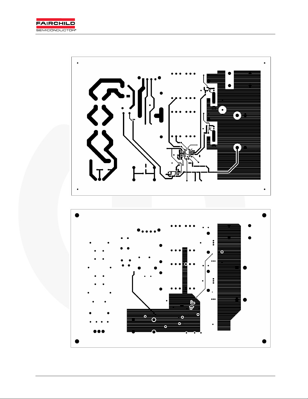
8. PCB Layout
Figure 5. First Layer (Top Side)
Figure 6. Second Layer (Plane Layer)
© 2010 Fairchild Semiconductor Corporation 10 FEB388_FAN9611/12 • Rev. 0.0.3
Page 11
www.fairchildsemi.com
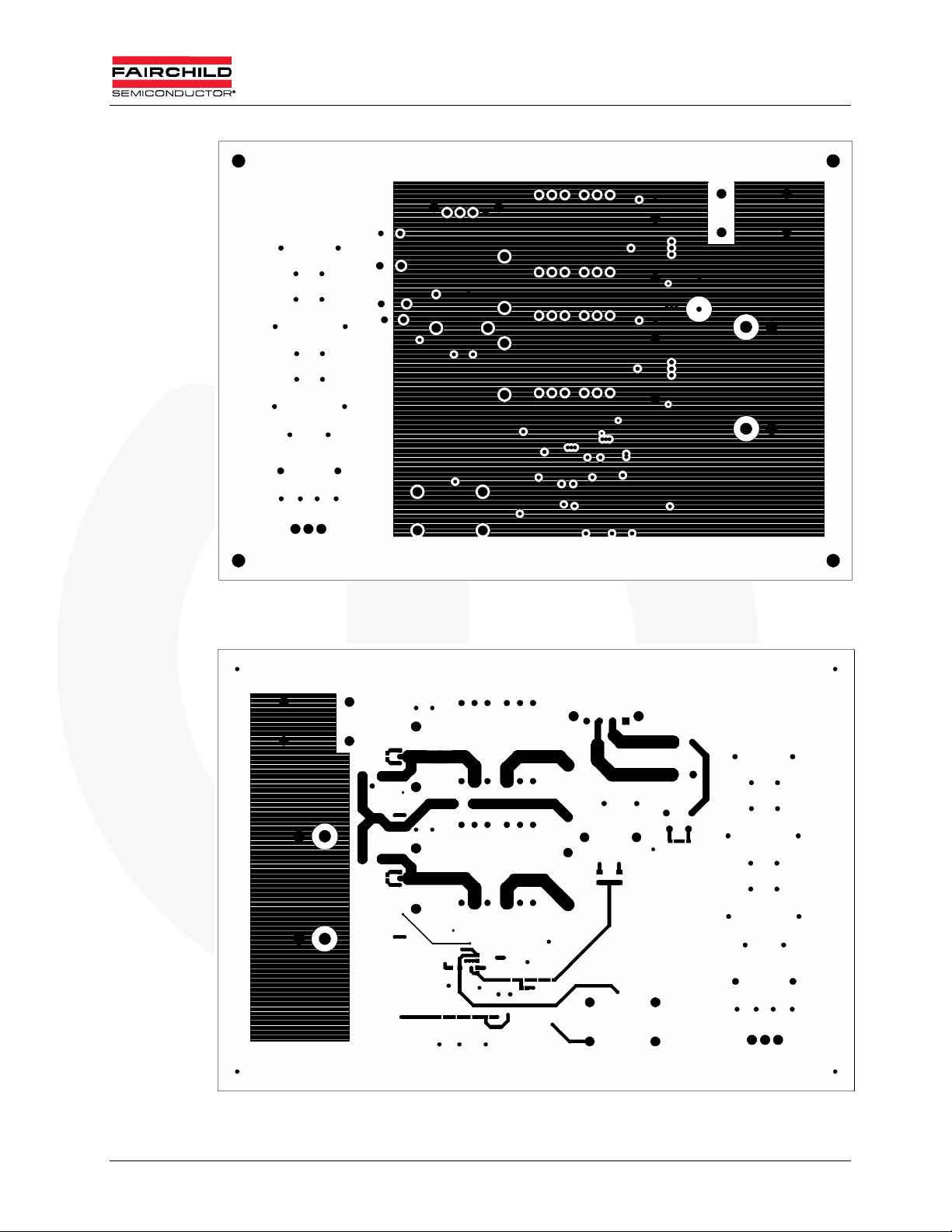
Figure 7. Third Layer (Ground Layer)
Figure 8. Fourth Layer (Bottom Side)
© 2010 Fairchild Semiconductor Corporation 11 FEB388_FAN9611/12 • Rev. 0.0.3
Page 12
www.fairchildsemi.com
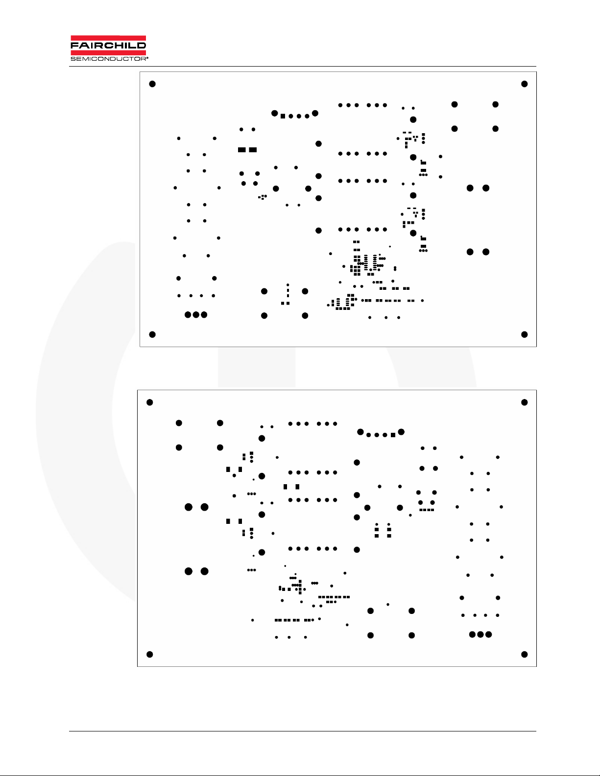
Figure 9. Top Solder Mask
Figure 10. Bottom Solder Mask
© 2010 Fairchild Semiconductor Corporation 12 FEB388_FAN9611/12 • Rev. 0.0.3
Page 13
www.fairchildsemi.com
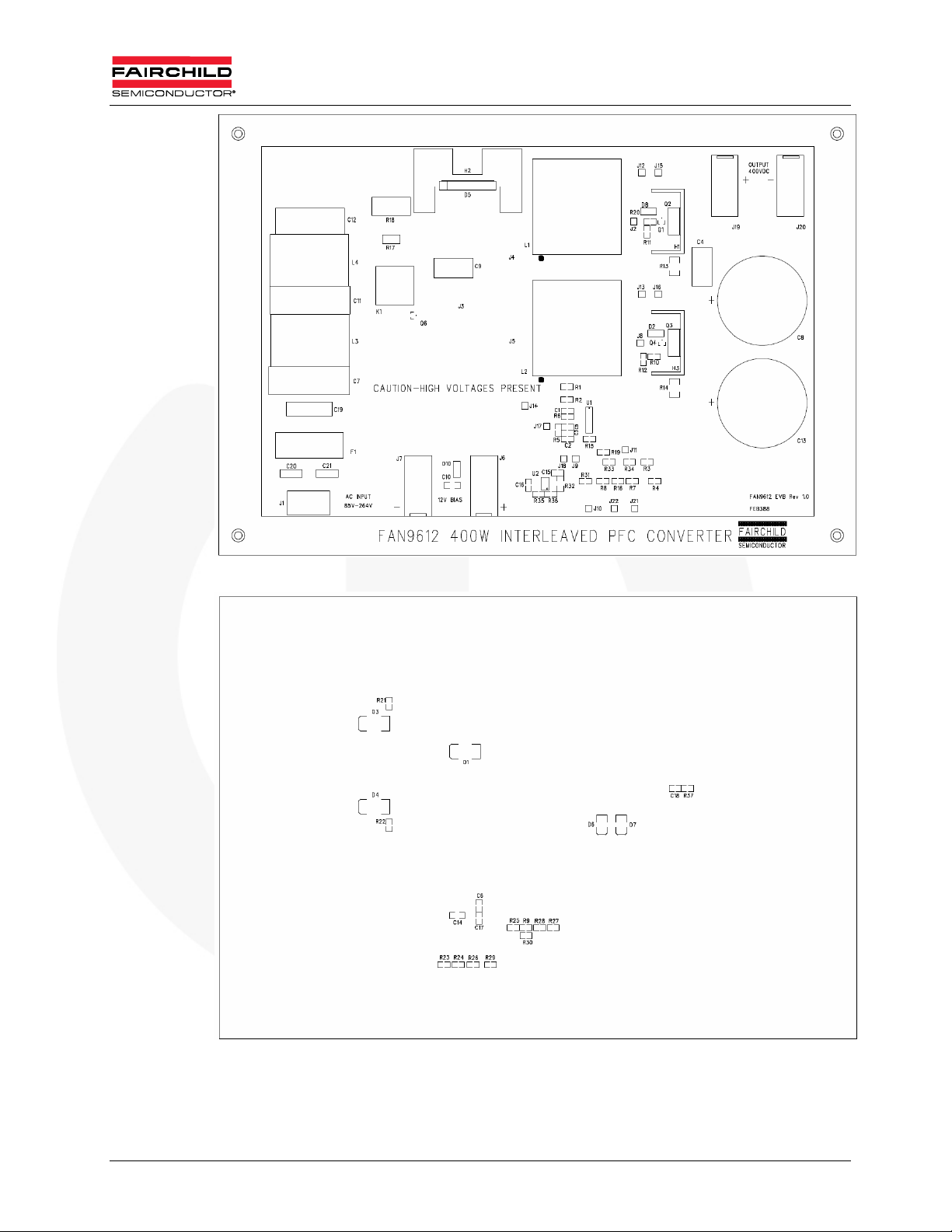
Figure 11. Top Silkscreen
Figure 12. Bottom Silkscreen
© 2010 Fairchild Semiconductor Corporation 13 FEB388_FAN9611/12 • Rev. 0.0.3
Page 14
www.fairchildsemi.com
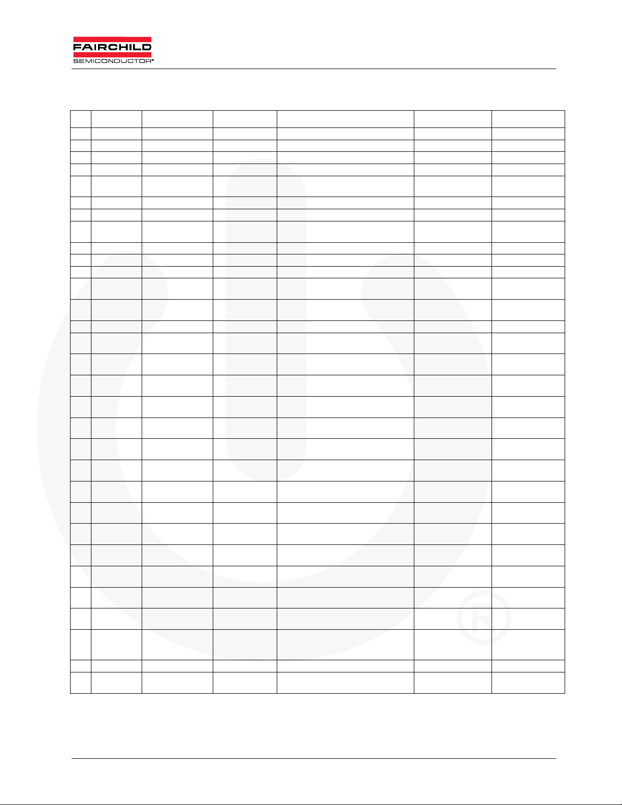
9. Bill of Materials (BOM)
Qty Referen ce Part Number Value Description Package Type Manufacturer
2 C1 C6 0.22µF CAP, SMD, CERAMIC, 25V, X7R 805 STD
1 C2 390nF CAP, SMD, CERAMIC, 25V, X7R 805 STD
2 C4 C9 ECWF2W154JAQ 150nF Cap, 400V, 5%, Polypropylene Radial, Thru-Hole Panasonic-ECG
1 C5 470nF CAP, SMD, CERAMIC,25V, X7R 805 STD
C7 C11
2
2 C8 C13 EETUQ2W221E 220µF Cap, Alum, Elect. Radial, Thru-Hole Panasonic
2 C10 C14 2.2µF CAP, SMD, CERAMIC, 25V, X7R 1206 STD
1 C12 HQX104K275R2 0.1µF, 275V
1 C15 15n CAP, SMD, CERAMIC,25V, X7R 805 STD
1 C16 0.1µF CAP, SMD, CERAMIC, 25V, X7R 805 STD
1 C18 1µF CAP, SMD, CERAMIC,50V, X5R 805 STD
1 C19
2 C20-21
1 C22 1nF CAP, SMD, CERAMIC, 25V, X7R 805 STD
3 D1 D3-4 S3J Diode, 600V, 3A, Std recovery SMC
2 D2 D8 MBR0540 Diode, Schottky,40V, 500mA SOD-123
1 D5 GBU8J Bridge Rectifier, 600V, 8A Thru-Hole
2 D6-7 ES1J DIODE FAST REC 1A 600V SMA
1 D10 MBR0530
1 F1 31.8201 Fuseholder, 5x20mm, 250VAC, 10A
2 H1 H3 534202B33453G
1 H2 639BG
1 J1 ED100/3DS Terminal Block, 5MM Vert., 3 Pos. Thru-hole
14
3 J3-5
2 J6 J19 571-0500
2 J7 J20 571-0100
2 L1-2 PA2975NL-5P4 200µH
2 L3-4 TRN-0197 Common Mode Choke Thru-Hole
2 Q1 Q4 ZXTP25020DFL Transistor, PNP, 20V, 1.5A SOT-23 Zetex
2 Q2-3 FDPF18N50
C23
J2 J8-18
J21-22
B32914A3474 470nF,330V Cap, 330VAC, 10%, Polypropylene Box, Thru-Hole EPCOS
PHE840MB
6100MB05R17
CS85-
B2GA471KYNS
3103-1-00-15-00-
00-08-0
Cap, X series 250VAC, 5%,
Polypropylene
0.1µF
470pF Cap, Ceramic, 250VAC, 10%, Y5P, Disc, Thru-hole TDK Corporation
Cap, X Type, 275VAC, 10%,
Polypropylene
DIODE SCHOTTKY 30V 500MA
SOD-123
Heatsink, 13.4degC/W, TO-220 with
Tab-Koolclip for Q2-3
TO-220 Heat sink for D5, Bridge
Rectifier
Probe-pin, Gold, 0.3" x 40mil dia.,
31mil mounting length
Jumper wire, #16, Insulated, for
current probe measurement
Banana Jack, .175, Horizontal,
Insulated_RED
Banana Jack, .175, Horizontal,
Insulated_BLK
Coupled Inductor, PQ3230, Pri-30T,
Sec-3T
MOSFET, NCH, 500V, 18A, 0.265
Ohm
Box, Thru-Hole
Box, Axial KEMET
SOD-123
PCB mount, Thruhole
1"x0.475"x1.18" Aavid Thermalloy
1.65"x1.5" Aavid Thermalloy
Thru-Hole Mill-Max
Thru-Hole Custom
Thru-Hole Deltron
Thru-Hole Deltron
Thru-Hole Pulse Electronics
TO-220
Fuhjyyu Electronic
Industrial Co.
Fairchild
Semiconductor
Fairchild
Semiconductor
Fairchild
Semiconductor
Fairchild
Semiconductor
Fairchild
Semiconductor
Schurter Inc
On Shore
Technology, Inc.
SEN HUEI
INDUSTRIAL
CO.,LTD
Fairchild
Semiconductor
Continued on following page…
© 2010 Fairchild Semiconductor Corporation 14 FEB388_FAN9611/12 • Rev. 0.0.3
Page 15
www.fairchildsemi.com
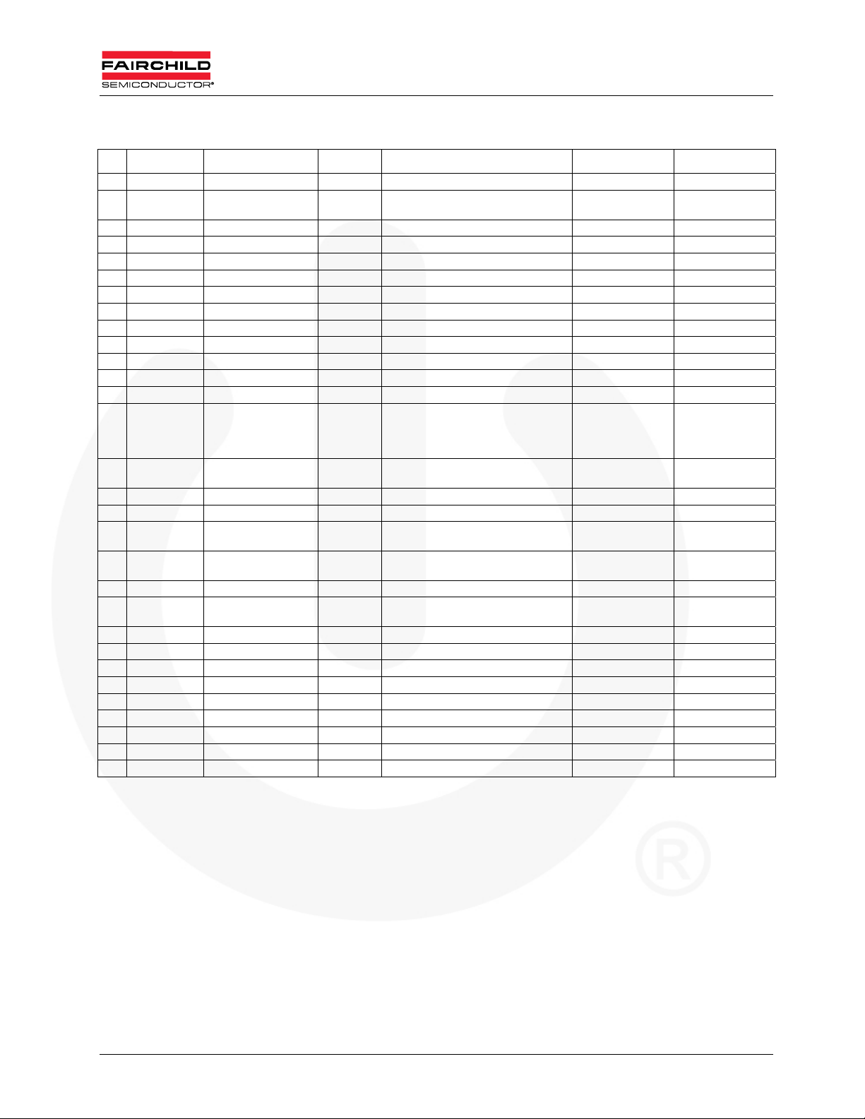
BOM (Continued)
Qty Reference Part Number Value Description Package Type Manufacturer
2 R1-2 47kΩ RES, SMD, 1/8W 805 STD
R3 R9 R27-
6
28 R33-34
1 R4 332kΩ RES, SMD, 1/8W 805 STD
1 R5 68kΩ RES, SMD, 1/8W 805 STD
1 R6 100kΩ RES, SMD, 1/8W 805 STD
2 R7-8 340kΩ RES, SMD, 1/8W 805 STD
2 R10 R20 100Ω RES, SMD, 1/8W 805 STD
2 R11-12 15Ω RES, SMD, 1/8W 805 STD
1 R15 DNP RES, SMD, 1/8W 805 STD
1 R16 49.9Ω RES, SMD, 1/8W 805 STD
1 R17 0 RES, SMD, 1/2W 2010 STD
1 R18 B57237S0509M000 5Ω Thermistor, 5Ω Thru-Hole EPCOS
1 R19 14.7kΩ RES, SMD, 1/8W 805 STD
1 inserted
into each
4
corner of
PCB
1 1 at D5, H2 3103
1 1 at D5, H2 MLWZ 003 Split Lock Washer, Metric M 3 Zinc Washer B&F Fastener
1 1 at D5, H2 HNZ440 Nut Hex, #4-40 Zinc Nut B&F Fastener
1 1 at D5, H2 PMS 440 0050 PH
1 PWB
2 R1-2 47kΩ RES, SMD, 1/8W 805 STD
R3 R9 R27-
6
28 R33-34
1 R4 332kΩ RES, SMD, 1/8W 805 STD
1 R5 68kΩ RES, SMD, 1/8W 805 STD
1 R6 100kΩ RES, SMD, 1/8W 805 STD
2 R7-8 340kΩ RES, SMD, 1/8W 805 STD
2 R10 R20 100Ω RES, SMD, 1/8W 805 STD
2 R11-12 15Ω RES, SMD, 1/8W 805 STD
2 R13-14 0.022Ω RES, SMD, 1/2W 1812 STD
1 R15 DNP RES, SMD, 1/8W 805 STD
1 R16 49.9Ω RES, SMD, 1/8W 805 STD
FEB388 Rev. 0.0.1
Note:
2. DNP = Do not populate. STD = standard components
665kΩ RES, SMD, 1/8W 805 STD
LCBS-12-01
FAN9611/12
665kΩ RES, SMD, 1/8W 805 STD
FEB388 PWB, 9.8" x 6.8" PWB
LOCKING BOARD SUPPORT 3/4",
1 for each PCB corner
Nylon Shoulder Washer #4x0.187",
Black
Screw Machine Phillips, 4-40x1/2"
Zinc
Standoff
Washer
Screw B&F Fastener
Richco Plastic
Company
Keystone
Electronics
Fairchild
Semiconductor
© 2010 Fairchild Semiconductor Corporation 15 FEB388_FAN9611/12 • Rev. 0.0.3
Page 16
www.fairchildsemi.com
10. Test Results
10.1. Startup
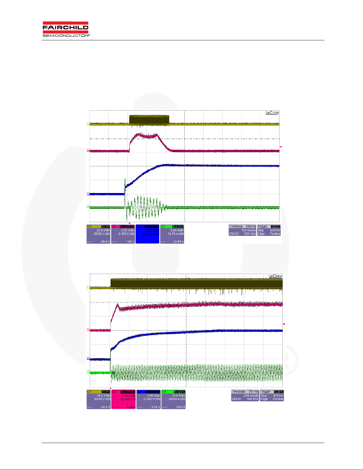
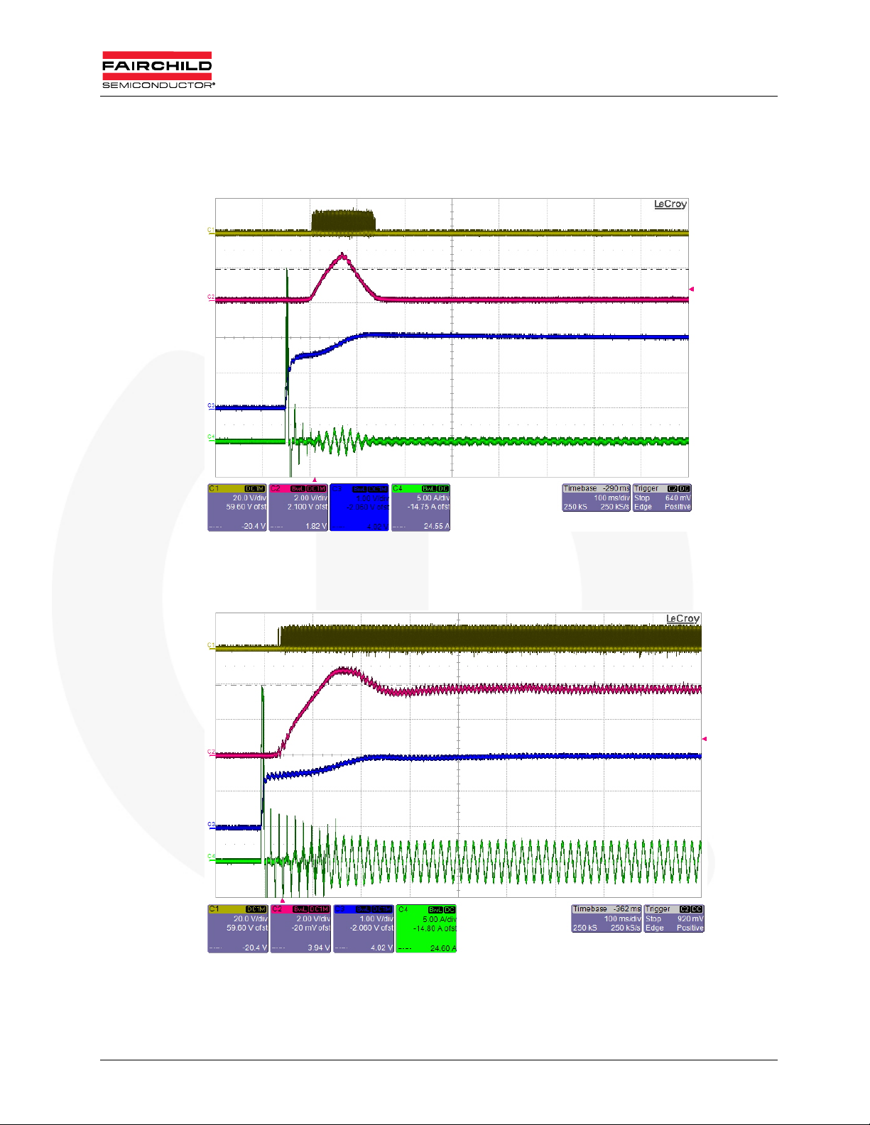
Figure 13 and Figure 14 show the startup operation at 115VAC line voltage for no-load and
full-load condition, respectively. Due to the closed-loop soft-start, almost no overshoot is
observed for no-load startup and full-load startup.
Gate Drive 1
COMP
Voltage
Output
Voltage
Line
Current
Gate Drive 1
COMP
Voltage
Output
Voltage
Line
Current
CH1: Gate Drive 1 Voltage (20V/div), CH2: COMP Voltage (2V/div),
CH3: Output Voltage (200V/div), CH4: Line Current (5A/div), Time (100ms/div)
Figure 13. No-Load Startup at 115V
CH1: Gate Drive 1 Voltage (20V/div), CH2: COMP Voltage (2V/div),
CH3: Output Voltage (200V/div), CH4: Line Current (10A/div), Time (200ms/div)
Figure 14. Full-Load Startup at 115V
AC
AC
© 2010 Fairchild Semiconductor Corporation 16 FEB388_FAN9611/12 • Rev. 0.0.3
Page 17
Gate Drive 1
COMP
Voltage
Output
Voltage
Line
Current
www.fairchildsemi.com
Figure 15 and Figure 16 show the startup operation at 230V
full-load conditions, respectively. Due to the closed-loop soft-start, almost no overshoot is
observed for no-load startup and full-load startup.
line voltage for no-load and
AC
Gate Drive 1
COMP
Voltage
Output
Voltage
Line
Current
CH1: Gate Drive 1 Voltage (20V/div), CH2: COMP Voltage (2V/div),
CH3: Output Voltage (200V/div), CH4: Line Current (5A/div), Time (100ms/div)
Figure 15. No-Load Startup at 230V
AC
CH1: Gate Drive 1 Voltage (20V/div), CH2: COMP Voltage (2V/div),
CH3: Output Voltage (200V/div), CH4: Line Current (5A/div), Time (100ms/div)
Figure 16. Full-Load Startup at 230V
© 2010 Fairchild Semiconductor Corporation 17 FEB388_FAN9611/12 • Rev. 0.0.3
AC
Page 18
www.fairchildsemi.com
10.2. Normal Operation
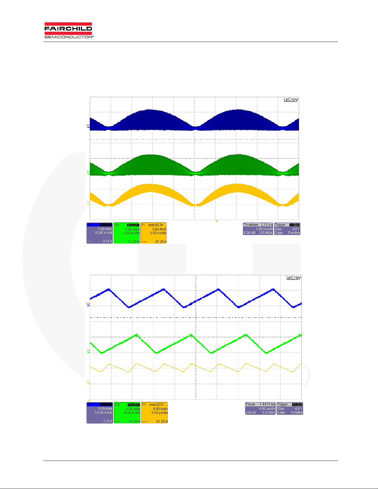
Figure 17 and Figure 18 show the two inductor currents and sum of two inductor currents
line voltage and full-load conditions. The sum of the inductor currents has
AC
I
L1
I
L2
I
L1
at 115V
relatively small ripple due to the ripple cancellation of interleaving operation.
+ IL2
I
L1
I
L2
I
L1
+ IL2
CH3: Inductor L1 Current (5A/div), CH4: Inductor L2 Current (5A/div),
F1: Sum of Two Inductor Current (5A/div), Time (2ms/div)
Figure 17. Inductor Current Waveforms at Full-Load and 115V
AC
CH3: Inductor L1 Current (5A/div), CH4: Inductor L2 Current (5A/div),
F1: Sum of Two Inductor Current (5A/div), Time (5s/div)
Figure 18. Zoom of Inductor Current Waveforms of Figure 17 at Peak of Line Voltage
© 2010 Fairchild Semiconductor Corporation 18 FEB388_FAN9611/12 • Rev. 0.0.3
Page 19
I
L1
I
L2
I
L1
+ IL2
www.fairchildsemi.com
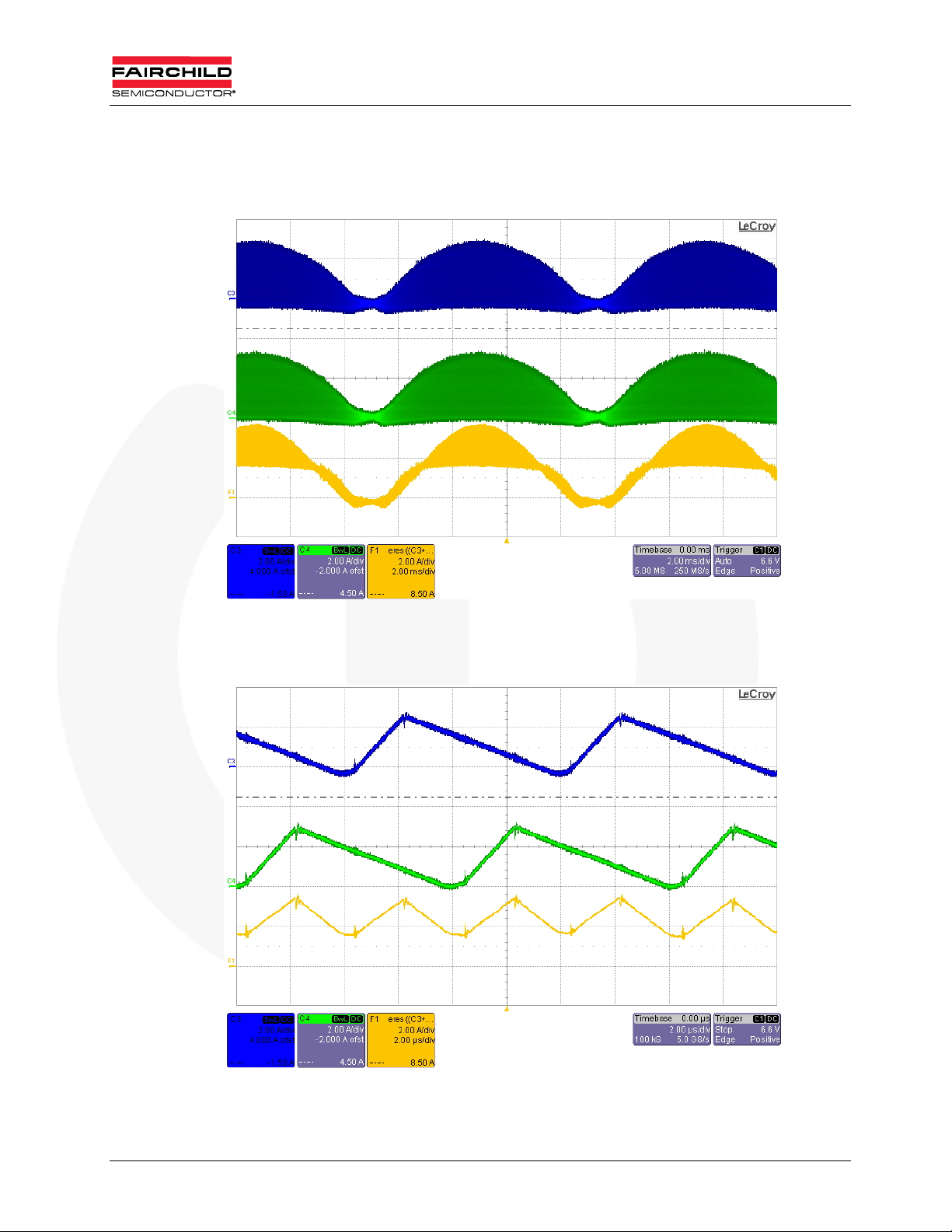
Figure 19 and Figure 20 show the two inductor currents and sum of two
inductor currents at 230V
sum of the inductor currents has relatively small ripple due to the ripple
cancellation of interleaving operation.
line voltage and full-load conditions. The
AC
I
L1
I
L2
I
L1
+ IL2
CH3: Inductor L1 Current (2A/div), CH4: Inductor L2 Current (2A/div),
F1: Sum of Two Inductor Current (2A/div), Time (2ms/div)
Figure 19. Inductor Current Waveforms at Full-Load and 230V
AC
CH3: Inductor L1 Current (2A/div), CH4: Inductor L2 Current (2A/div),
F1: Sum of Two Inductor Current (2A/div), Time (2s/div)
Figure 20. Zoom of Inductor Current Waveforms of Figure 19 at Peak of Line Voltage
© 2010 Fairchild Semiconductor Corporation 19 FEB388_FAN9611/12 • Rev. 0.0.3
Page 20
www.fairchildsemi.com
V
V
V
V
10.3. Line Transient
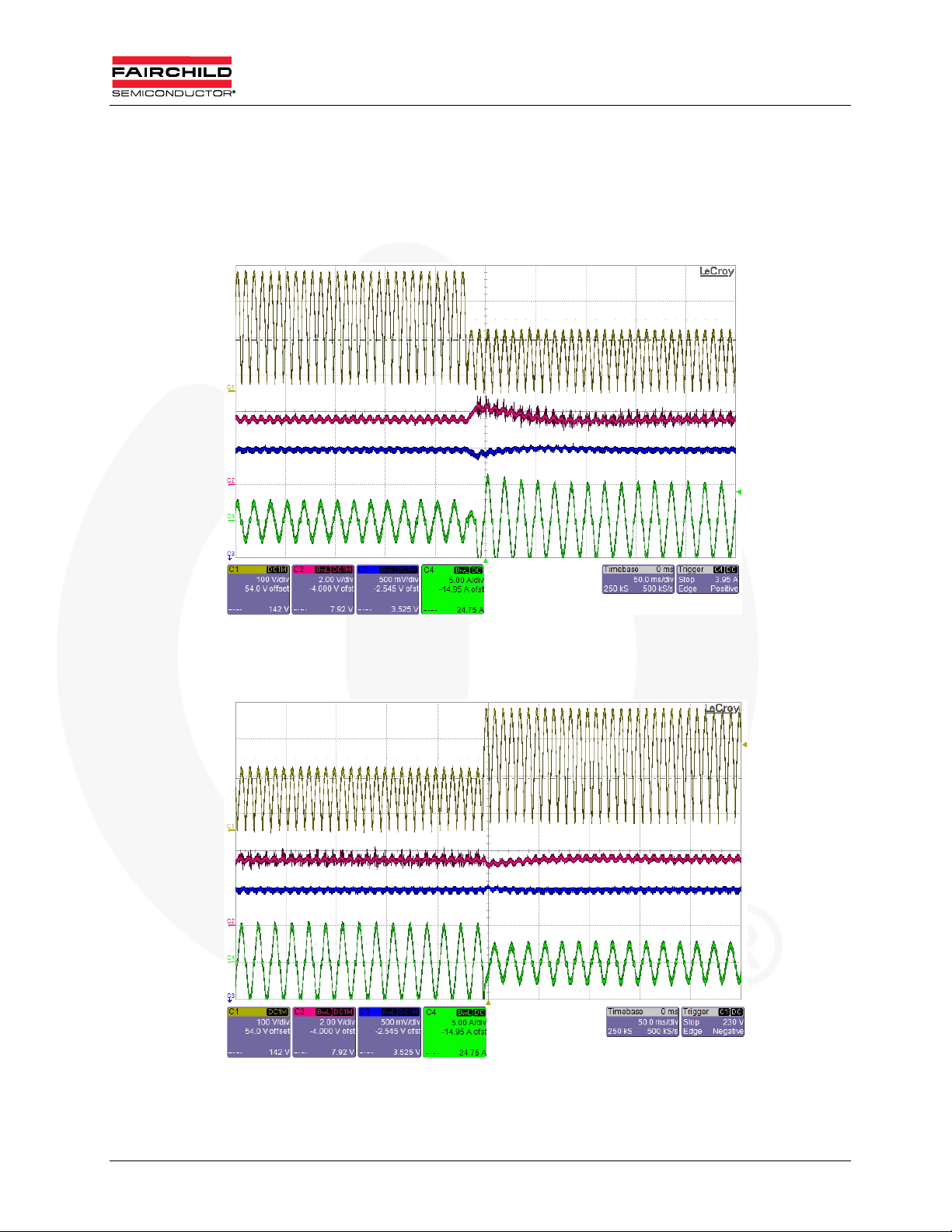
Figure 21 and Figure 22 show the line transient operation and minimal effect on output
voltage due to the line feed-forward function. When the line voltage changes from
230V
observed. When the line voltage changes from 115V
undershoot is observed.
Rectified
Line
Voltage
Line
Current
to 115VAC, about 20V (5% of nominal output voltage) voltage undershoot is
AC
to 230VAC, almost no voltage
AC
Rectified
Line
Voltage
Line
Current
CH1: Rectified Line Voltage (100V/div), CH2: COMP Voltage (2V/div),
CH3: Output Voltage (100V/div), CH4: Line Current (5A/div), Time (50ms/div)
Figure 21. Line Transient Response at Full-Load Condition (230V
CH1: Rectified Line Voltage (100V/div), CH2: COMP Voltage (2V/div),
CH3: Output Voltage (100V/div), CH4: Line Current (5A/div), Time (50ms/div)
Figure 22. Line Transient Response at Full-Load Condition (115V
115VAC)
AC
230VAC)
AC
© 2010 Fairchild Semiconductor Corporation 20 FEB388_FAN9611/12 • Rev. 0.0.3
Page 21

www.fairchildsemi.com
V
V
10.4. Load Transient
Figure 23 and Figure 24 show the load-transient operation. When the output load changes
from 100% to 0%, 26V (6.5% of nominal output voltage) voltage overshoot is observed.
When the output load changes from 0% to 100%, 43V (11% of nominal output voltage)
voltage undershoot is observed.
Rectified
Line
Voltage
Line
Current
Rectified
Line
Voltage
Line
Current
CH2: Rectified line voltage (100V/div), CH3: Output voltage (100V/div),
CH4: Line current (5A/div), Time (50ms/div)
Figure 23. Load Transient Response at 230VAC (Full Load No Load)
CH2: Rectified Line Voltage (100V/div), CH3: Output Voltage (100V/div),
CH4: Line Current (5A/div), Time (50ms/div)
Figure 24. Load Transient Response at 230VAC (No Load Full Load)
© 2010 Fairchild Semiconductor Corporation 21 FEB388_FAN9611/12 • Rev. 0.0.3
Page 22
www.fairchildsemi.com
10.5. Brownout Protection
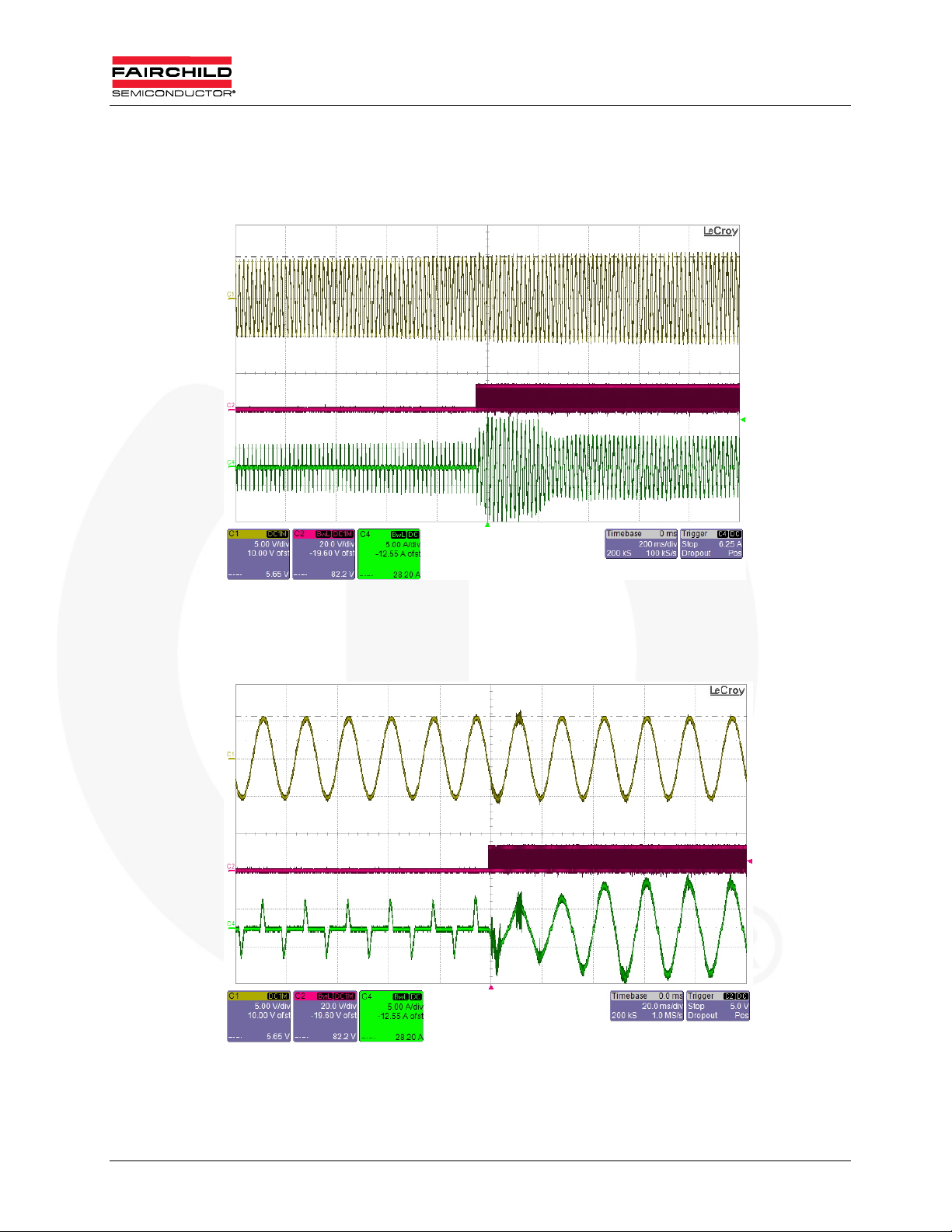
Figure 25 and Figure 26 show the startup operation at slowly increasing line voltage.
The power supply starts up when the line voltage reaches around 78V
Line
Voltage
Gate
Drive 1
Line
Current
AC
.
Line
Voltage
Gate
Drive 1
Line
Current
CH1: Line Voltage (100V/div), CH2: Gate Drive 1 Voltage (20V/div),
CH4: Line Current (5A/div), Time (200ms/div)
Figure 25. Startup Slowly Increasing the Line Voltage
CH1: Line Voltage (100V/div), CH2: Gate Drive 1 Voltage (20V/div),
CH4: Line Current (5A/div), Time (20ms/div)
Figure 26. Shutdown Slowly Decreasing the Line Voltage
© 2010 Fairchild Semiconductor Corporation 22 FEB388_FAN9611/12 • Rev. 0.0.3
Page 23
Line
Voltage
Gate
Drive 1
Line
Current
www.fairchildsemi.com
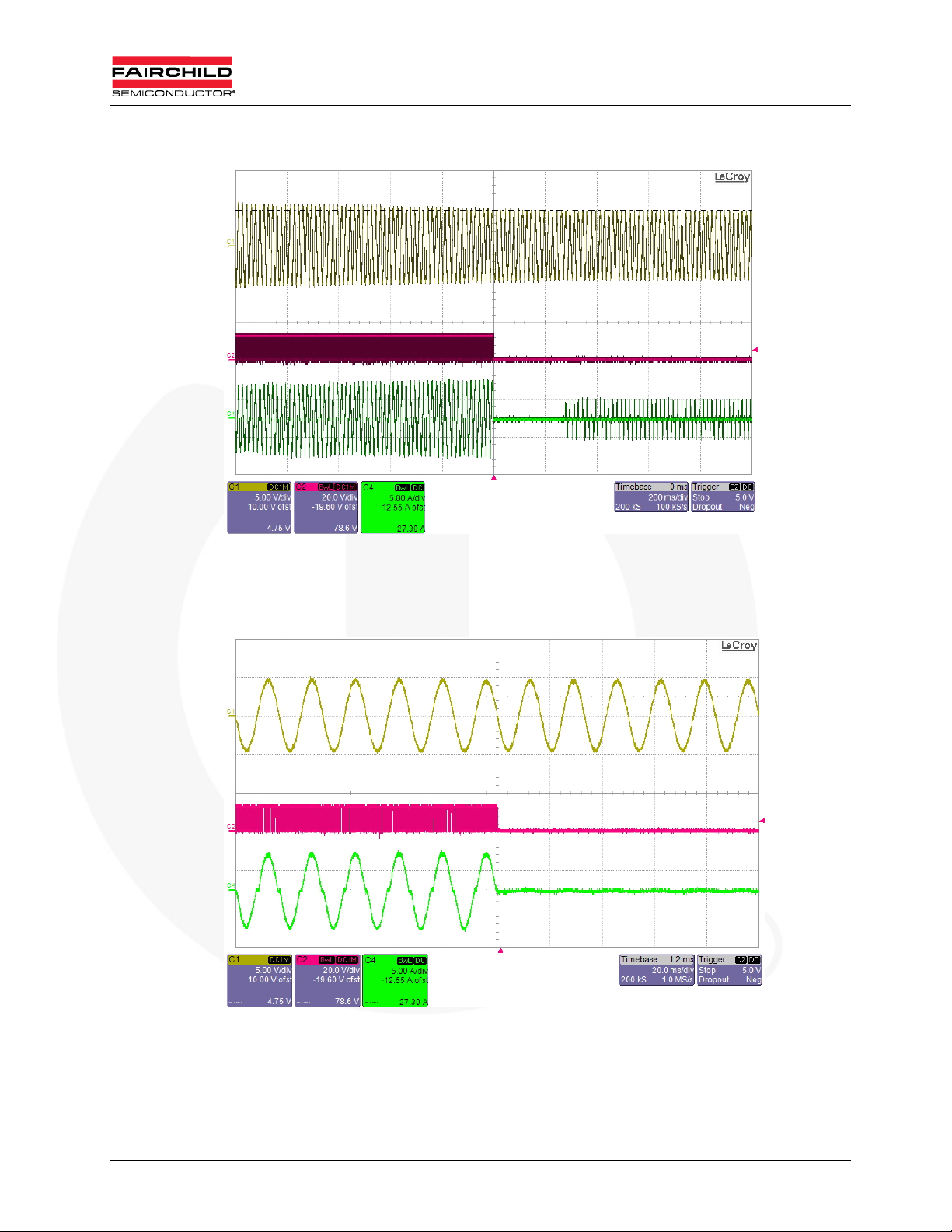
Figure 27 and Figure 28 show the shutdown operation at slowly decreasing line voltage.
The power shuts down when line voltage drops below 68V
CH1: Line Voltage (100V/div), CH2: Gate Drive 1 Voltage (20V/div),
CH4: Line Current (5A/div), Time (200ms/div)
Figure 27. Startup Slowly Increasing the Line Voltage
AC
.
Line
Voltage
Gate
Drive 1
Line
Current
CH1: Line Voltage (100V/div), CH2: Gate Drive 1 Voltage (20V/div),
CH4: Line Current (5A/div), Time (20ms/div)
Figure 28. Shutdown Slowly Decreasing the Line Voltage
© 2010 Fairchild Semiconductor Corporation 23 FEB388_FAN9611/12 • Rev. 0.0.3
Page 24

www.fairchildsemi.com
10.6. Phase Management
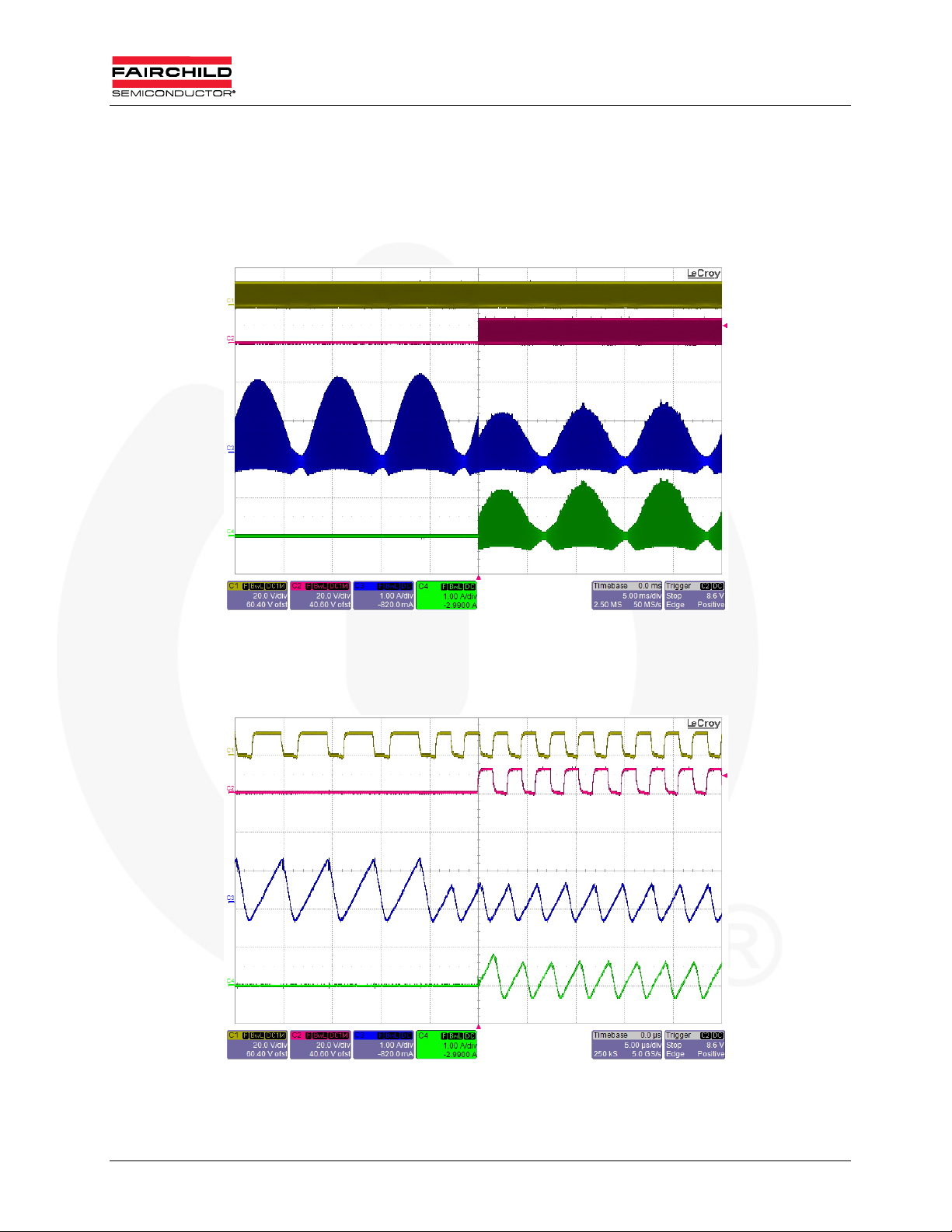
Figure 29 and Figure 30 show the phase-shedding waveforms. As observed, when the gate
drive signal of Channel 2 is disabled, the duty cycle of Channel 1 gate drive signal is
doubled to minimize the line current glitch and guarantee smooth transient.
Gate
Drive 1
Gate
Drive 2
I
L1
I
L2
Gate
Drive 1
Gate
Drive 2
I
L1
I
L2
CH1: Gate Drive 1 Voltage (20V/div), CH2: Gate Drive 2 Voltage (20V/div),
CH3: Inductor L1 Current (1A/div), CH4: Inductor L2 Current (1A/div), Time (5ms/div)
Figure 29. Phase-Shedding Operation
CH1: Gate Drive 1 Voltage (20V/div), CH2: Gate Drive 2 Voltage (20V/div),
CH3: Inductor L1 Current (1A/div), CH4: Inductor L2 Current (1A/div), Time (5µs/div)
Figure 30. Phase-Shedding Operation (Zoomed-in Timescale)
© 2010 Fairchild Semiconductor Corporation 24 FEB388_FAN9611/12 • Rev. 0.0.3
Page 25
www.fairchildsemi.com
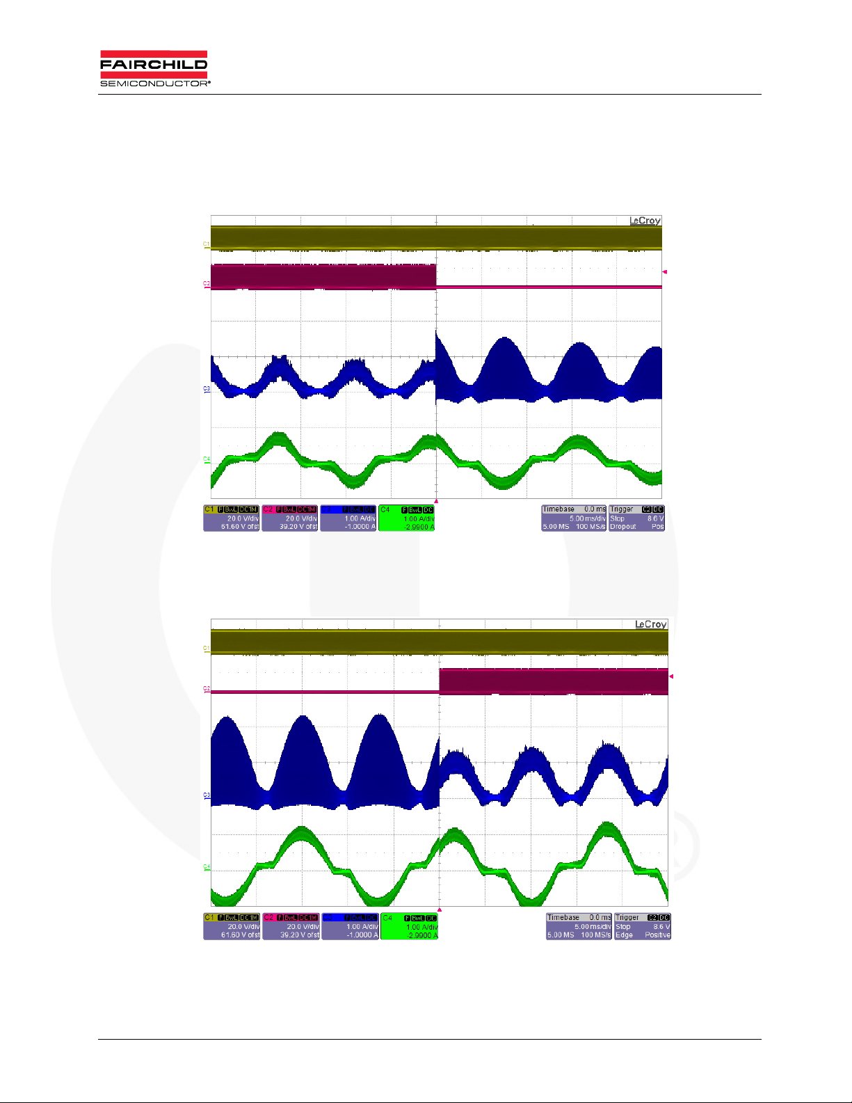
Figure 31 and Figure 32 show the phase-adding waveforms. As observed, just before the
channel 2 gate drive signal is enabled, the duty cycle of Channel 1 gate drive signal is
halved to minimize the line current glitch and guarantee smooth transient. In Figure 32, the
first pulse of gate drive 2 during the phase-adding operation is skipped to ensure 180
degree out-of-phase interleaving operation during transient.
Gate
Drive 1
Gate
Drive 2
I
L1
I
L2
Gate
Drive 1
Gate
Drive 2
I
L1
I
L2
CH1: Gate Drive 1 Voltage (20V/div), CH2: Gate Drive 2 Voltage (20V/div),
CH3: Inductor L1 Current (1A/div), CH4: Inductor L2 Current (1A/div), Time (5ms/div)
Figure 31. Phase-Adding Operation
CH1: Gate Drive 1 Voltage (20V/div), CH2: Gate Drive 2 Voltage (20V/div),
CH3: Inductor L1 Current (1A/div), CH4: Inductor L2 Current (1A/div), Time (5µs/div)
Figure 32. Phase-Adding Operation (Zoomed-in Timescale)
© 2010 Fairchild Semiconductor Corporation 25 FEB388_FAN9611/12 • Rev. 0.0.3
Page 26
Gate
Drive 1
Gate
Drive 2
I
+ IL1
L1
Line
Current
www.fairchildsemi.com
Figure 33 and Figure 34 show the sum of two-inductor current and line current for phase
shedding and adding, respectively. The small line-current glitch during phase
management exists because the actual average value of inductor current is less than half
of the peak value due to the negative portion of inductor current, as shown in Figure 30
and Figure 32. However, the phase management takes place at relatively light-load
condition and the effect of this phenomenon is negligible.
Gate
Drive 1
Gate
Drive 2
+ IL1
I
L1
Line
Current
CH1: Gate Drive 1 Voltage (20V/div), CH2: Gate Drive 2 Voltage (20V/div),
CH3: Sum of Two Inductor Currents (1A/div), CH4: Line Current (1A/div), Time (5ms/div)
Figure 33. Phase Shedding and L ine Current
CH1: Gate Drive 1 Voltage (20V/div), CH2: Gate Drive 2 Voltage (20V/div),
CH3: Sum of Two Inductor Currents (1A/div), CH4: Line Current (1A/div), Time (5ms/div)
Figure 34. Phase Adding Operation and Line Current
© 2010 Fairchild Semiconductor Corporation 26 FEB388_FAN9611/12 • Rev. 0.0.3
Page 27
www.fairchildsemi.com
10.7. Efficiency
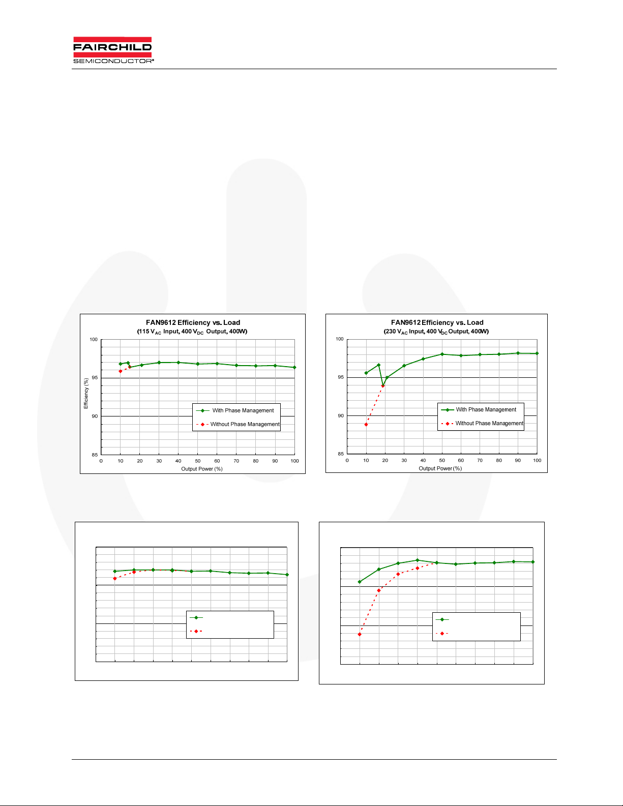
Figure 35 through Figure 38 show the measured efficiency of the 400W evaluation board
with and without phase management at input voltages of 115V
management improves the efficiency at light load by up to 7%, depending on the line
voltage and load condition. The phase management thresholds on the test evaluation board
are around 15% of the nominal output power (Figure 35 and Figure 36). They can be
adjusted upwards to achieve a more desirable efficiency profile (Figure 37 and Figure 38)
by increasing the MOT resistor.
Since phase shedding reduces the switching loss by effectively decreasing the switching
frequency at light load, a greater efficiency improvement is achieved at 230V
switching losses dominate. Relatively less improvement is obtained at 115V
MOSFET is turned on with zero voltage and switching losses are negligible.
The efficiency measurements include the losses in the EMI filter as well as cable loss;
however, the power consumption of the control IC (<< 1W) is not included since an
external power supply is used for V
DD
and 230VAC. Phase
AC
, where
AC
since the
AC
.
Figure 35. Measured Efficiency at 115VAC
(Default Thresholds)
FAN9612 Effi ciency vs. L oad
100
95
Efficiency (%)
90
85
0 102030405060708090100
(115 VAC Input, 400 VDC Output, 400W)
With Phase Management
Witho ut Phase Manag ement
Output Power (%)
Figure 37. Measured Efficiency at 115VAC
(Adjusted Thresholds)
Efficiency (%)
Figure 36. Measured Efficiency at 230V
AC
(Default Thresholds)
FAN9612 Efficiency vs. Load
100
95
Efficiency (%)
90
85
0 102030405060708090100
Figure 38. Measured Efficiency at 230V
(230 VAC Input, 400 VDC Output, 400W)
With Phase Management
Without Phase Management
Output Po wer (%)
AC
(Adjusted Thresholds)
© 2010 Fairchild Semiconductor Corporation 27 FEB388_FAN9611/12 • Rev. 0.0.3
Page 28
www.fairchildsemi.com
10.8. Harmonic Distortion and Power Factor
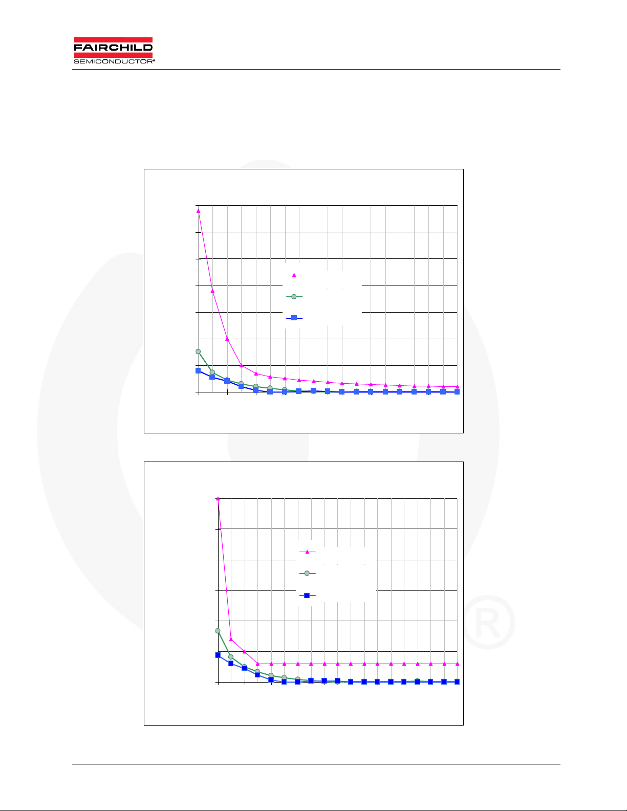
Figure 39 and Figure 40 compare the measured harmonic current with EN61000 class D
and C, respectively, at input voltages of 115V
PC power, while Class C is applied to lighting applications. As can be observed, both
regulations are met with sufficient margin.
EN61000 Class-D
1.4
1.2
1.0
and 230VAC. Class D is applied to TV and
AC
0.8
0.6
0.4
Harmonic Current (A)
0.2
0.0
3 7 11 15 19 23 27 31 35 39
EN61000-D
115V
AC
230V
AC
Harmonic or der
Figure 39. Measured Harmonic Current an d EN61000 Class-D Regulation
EN61000 Class-C
30%
25%
20%
15%
EN61000-C
115V
AC
230V
AC
10%
Harmonic Current
(% of Fundamental Cur r ent)
5%
0%
3 7 11 15 19 23 27 31 35 39
Harmonic order
Figure 40. Measured Harmonic Current and EN61000 Class-C Regulation
© 2010 Fairchild Semiconductor Corporation 28 FEB388_FAN9611/12 • Rev. 0.0.3
Page 29
www.fairchildsemi.com
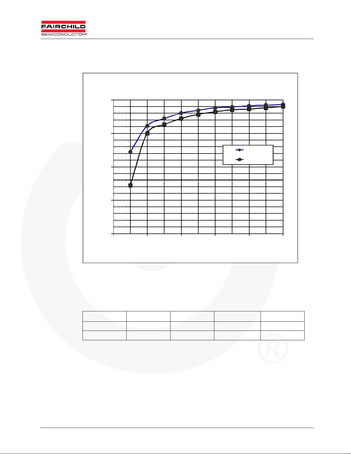
Figure 41 shows the measured power factors at input voltage of 115VAC and 230VAC. As
observed, high power factor above 0.98 is obtained from 100% to 50% load. Table 4 shows
the total harmonic distortion at input voltages of 115V
FAN9612 P ower Factor vs. Load
and 230VAC.
AC
100
95
)
%
(
r
o
t
c
a
F
r
e
w
o
P
90
115Vac
230Vac
85
80
0 20406080100
Output Power (%)
Figure 41. Measured Power Factor
Table 4. Total Harmonic Distortion (THD)
Line Voltage 100 % Load 75 % Load 50 % Load 25 % Load
115VAC
230VAC
9.68% 11.82% 15.87% 24.08%
11.36% 12.95% 15.30% 16.81%
© 2010 Fairchild Semiconductor Corporation 29 FEB388_FAN9611/12 • Rev. 0.0.3
Page 30
www.fairchildsemi.com
11. References
Datasheet: FAN9611 / FAN9612 – Interleaved Dual BCM PFC Controllers
AN-6086 – “Design Consideration for interleaved Boundary Conduction Mode
(BCM) PFC Using FAN9611 / FAN9612”
12. Ordering Information
Orderable Part Number Description
FEB388 FAN9611/FAN9612 400W Evaluation Board
13. Revision History
Date Rev. # Description
August 2010 0.0.1 Initial release
August 2010 0.0.2 Added PCB layout figures
February 2012 0.0.3 Corrected BOM
© 2010 Fairchild Semiconductor Corporation 30 FEB388_FAN9611/12 • Rev. 0.0.3
 Loading...