

Page 1
FAN7384
1
14-SOP
Half-Bridge Gate-Drive IC
FAN7384 — Half-Bridge Gate-Drive IC
July 2012
Features
Floating Channel for Bootstrap Operation to +600V
Typically 250mA/500mA Sourcing/Sinking Current
Driving Capability for Both Channels
Extended Allowable Negative V
Signal Propagation at VDD=VBS=15V
Matched Propagation Delay Below 50ns
Output In-Phase with Input Signal
3.3V and 5V Input Logic Compatible
Built-in Shoot-Through Prevention Logic
Built-in Common Mode dv/dt Noise Canceling Circuit
Built-in UVLO Functions for Both Channels
Built-in Cycle-by-Cycle Shutdown Function
Built-in Soft-Off Function
Built-in Bi-Directional Fault Function
Built-in Short-Circuit Protection Function
Swing to -9.8V for
S
Applications
Motor Inverter Driver
Normal Half-Bridge and Full-Bridge Driver
Switching Mode Power Supply
Description
The FAN7384 is a monolithic half-bridge gate-drive IC
designed for high voltage, high speed driving MOSFETs
and IGBTs operating up to +600V.
Fairchild’s high-voltage process and common-mode
noise canceling technique provide stable operation of
high-side drivers under high-dv/dt noise circumstances.
An advanced level-shift circuit allows high-side gate
driver operation up to V
The UVLO circuits prevent malfunction when VDD and
VBS are lower than the specified threshold voltage.
Output drivers typically source/sink 250mA/500mA,
respectively, which is suitable for half-bridge and fullbridge applications in motor drive systems.
= -9.8V (typical) for VBS =15V.
S
Ordering Information
Operating
Temperature
Part Number Package
14-Lead, Small Outline Integrated Circuit (SOIC),
FAN7384MX
Note:
1. The device passed wave soldering test by JESD22A-111.
© 2006 Fairchild Semiconductor Corporation www.fairchildsemi.com
FAN7384 Rev. 1.0.8
(1)
Non-JEDEC, .150 Inch Narrow Body, 225SOP
Range Packing Method
-40°C to +125°C Tape & Reel
Page 2
Typical Application Diagrams
U
V
W
W
3-Phase
Motor
Controller
V
U
HO
V
S
LO
V
B
V
DD
V
SL
LIN
HIN
HO
LO
LIN
HIN
HO
LO
LIN
HIN
UU
UL
VU
UL
WU
WL
V
DC
V
CC
CSC
CSC
CSC
SD SD SD
FO FO FO
GND
GND GND
V
DD
V
DD
V
SL
V
S
V
B
V
SL
V
S
V
B
FAN7384 Rev.03
FAN7384
FAN7384
FAN7384
Forward
V
DD
V
SL
HIN
M
Reverse
DC Motor
Controller
PHA
PHB
LIN
FAN7384
FAULT
HO
CSC
LO
HO
V
S
CSC
V
B
LO
HIN
HIN
FO
FO
SD
SD
FAN7384
SHUTDOWN
R
PULLUP
GND
GND
300K
300K
V
DC
V
CC
V
SL
V
DD
V
B
V
S
FAN7384 Rev.02
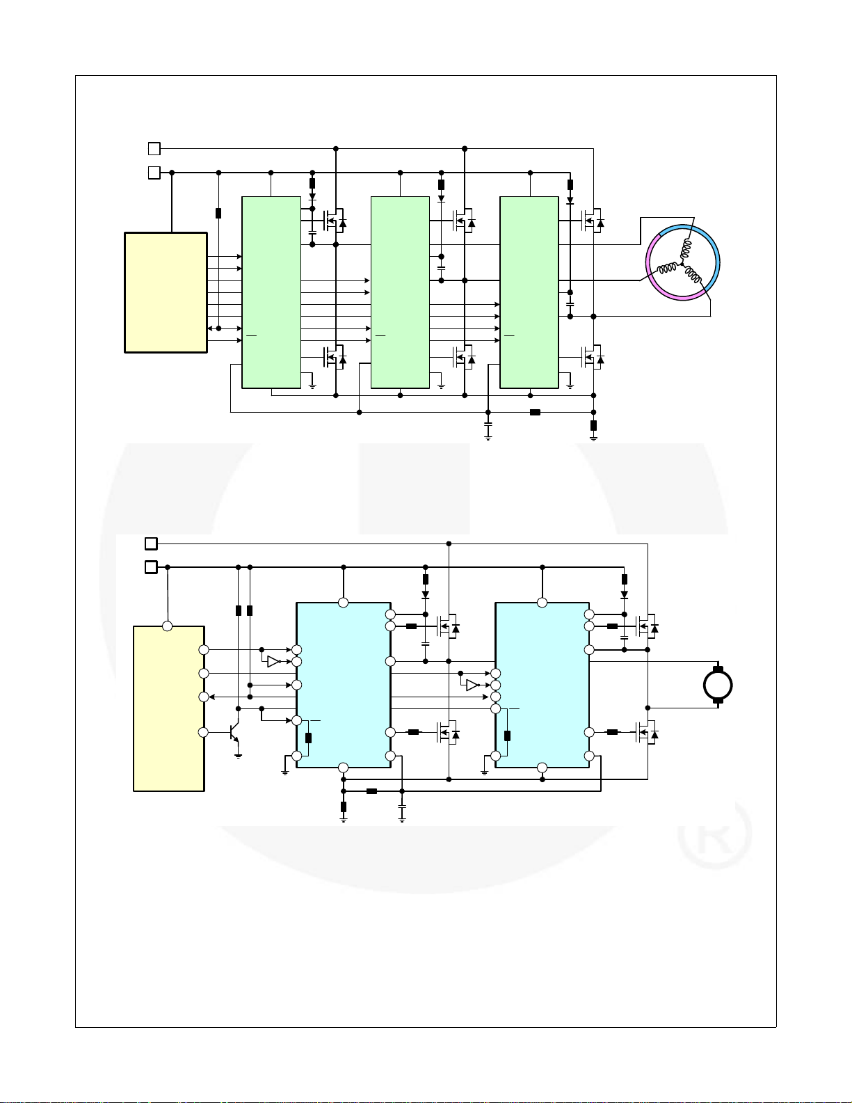
Figure 1. 3-Phase Motor Drive Application
FAN7384 — Half-Bridge Gate-Drive IC
© 2006 Fairchild Semiconductor Corporation www.fairchildsemi.com
FAN7384 Rev. 1.0.8 2
Figure 2. DC Motor Drive Application
Page 3
Internal Block Diagram
3
CSC
V
B
HO
HS(ON/OFF)
LS(ON/OFF)
1
5
2SD
SCHMITT
TRIGGER INPUT
SHOOT-THROUGH
PREVENTION
CONTROL LOGIC
6
0.5V
PULSE
GENERATOR
NOISE
CANCELLER
UVLO
14
12
R
R
S
Q
DRIVER
V
S
DRIVER
DELAY
SOFT-OFF
FAULT
LOGIC
8
4
9
13
7
V
DD
LO
V
SL
FO
GND
LIN
HIN
I
SOFT
GND/V
SL
LEVEL SHIFTER
UVLO
V
DD
_UVLO
V
DD
_UVLO
ONE-SHOT
TRIGGER
ONE-SHOT
TRIGGER
FAN7384 Rev.03
FAN7384 — Half-Bridge Gate-Drive IC
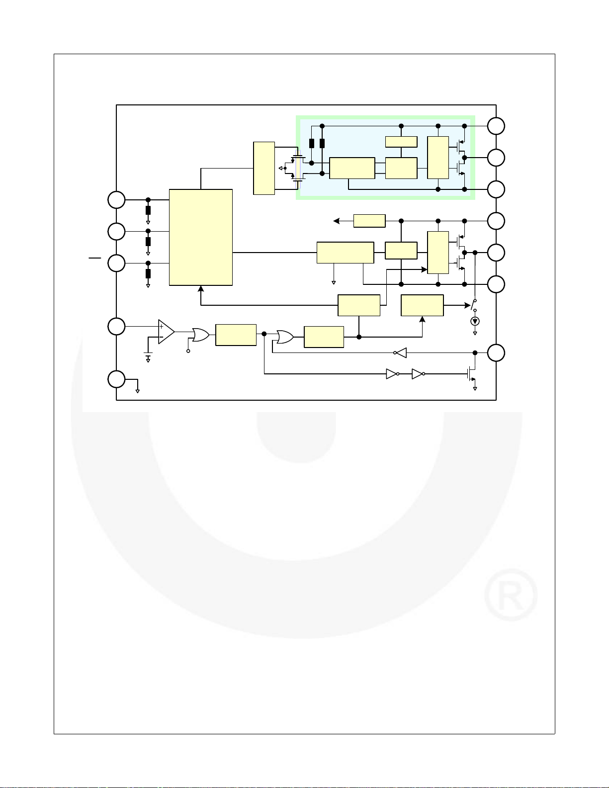
Figure 3. Functional Block Diagram
© 2006 Fairchild Semiconductor Corporation www.fairchildsemi.com
FAN7384 Rev. 1.0.8 3
Page 4
Pin Configuration
FAN7384 Rev.00
CSC
FO
GND
LO
NC
FAN7384
LIN
V
DD
V
S
HO
V
B
HIN
V
SL
NC
1
2
3
4
5
6
7
14
13
12
11
10
9
8
SD
FAN7384 — Half-Bridge Gate-Drive IC
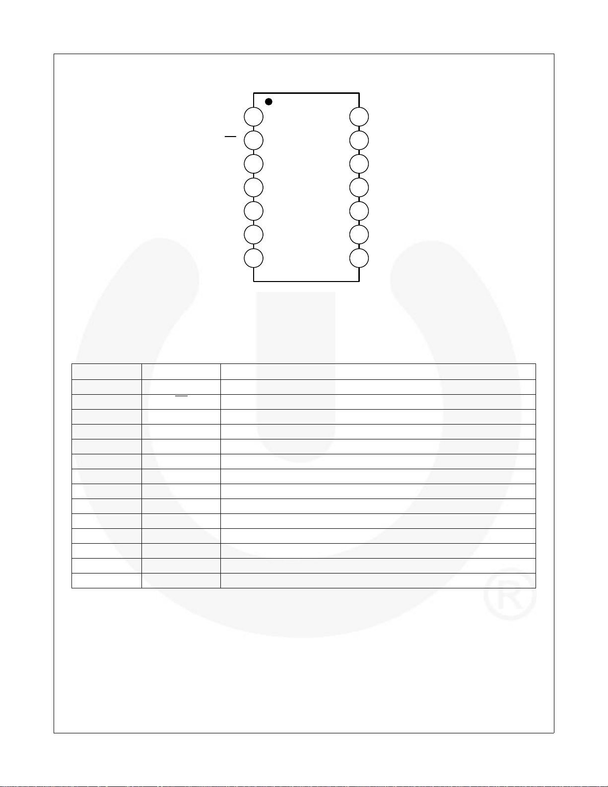
Figure 4. Pin Configuration (Top View)
Pin Definitions
Pin # Name Description
1 LIN Logic Input for low-side gate driver
2SD
3 HIN Logic Input for high-side gate driver
4V
DD
5 FO Bi-direction fault pin with open drain
6 CSC Short-circuit current detection input
7 GND Ground
8V
SL
9 LO Low-side gate driver output
10 NC Not connection
11 NC Not connection
12 V
S
13 HO High-side gate driver output
14 V
B
Shutdown control input with active low
Low-side power supply voltage
Low-side supply offset voltage
High-side floating supply offset voltage
High-side floating supply voltage
© 2006 Fairchild Semiconductor Corporation www.fairchildsemi.com
FAN7384 Rev. 1.0.8 4
Page 5
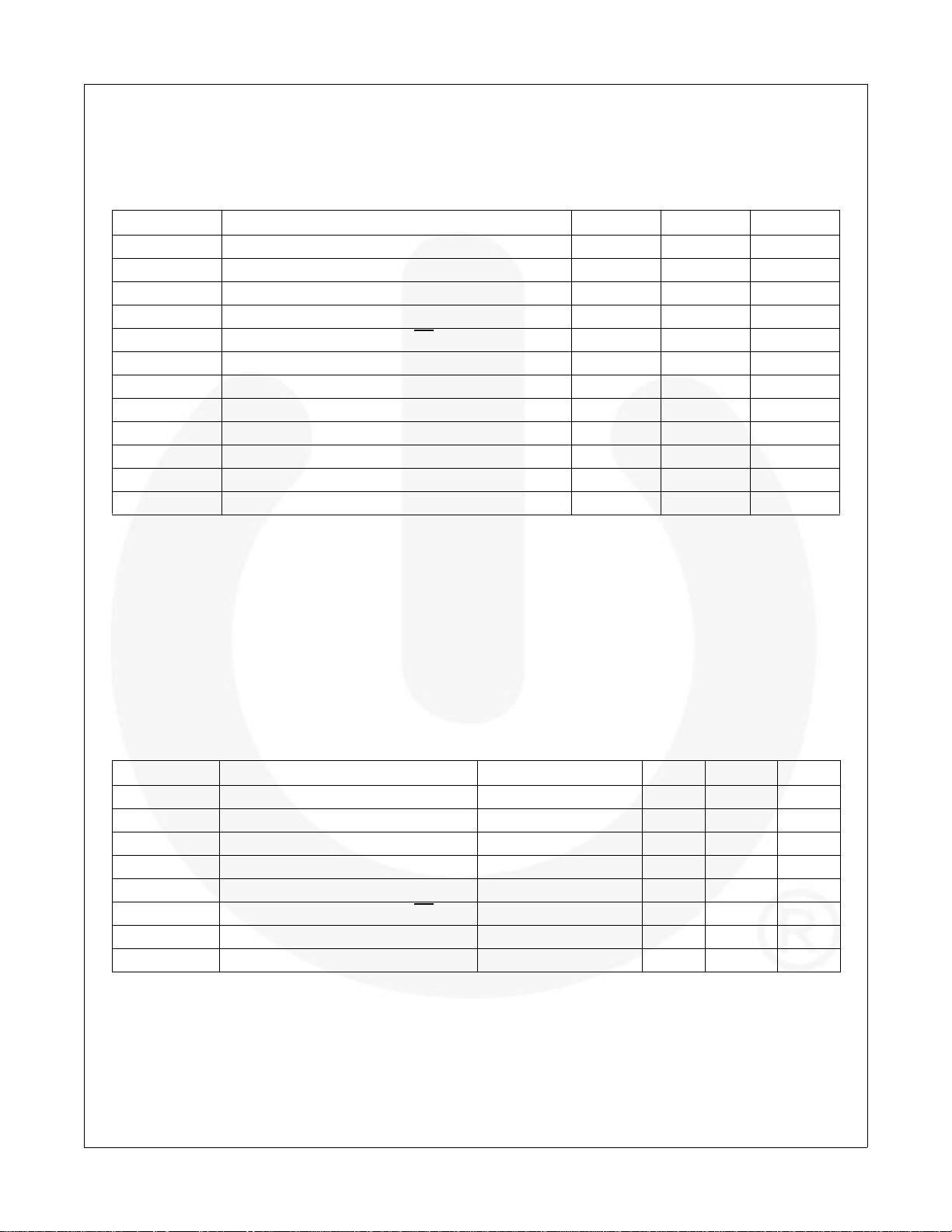
Absolute Maximum Ratings
Stresses exceeding the absolute maximum ratings may damage the device. The device may not function or be operable above the recommended operating conditions and stressing the parts to these levels is not recommended. In addition, extended exposure to stresses above the recommended operating cond itions may affect device reliability. The
absolute maximum ratings are stress ratings only. T
Symbol Parameter Min. Max. Unit
V
S
V
B
V
HO
V
DD
V
IN
V
CSC
V
FO
/dt Allowable offset voltage slew rate 50 V/ns
dV
S
(2)(3)(4)
P
D
JA
T
J
T
S
Notes:
2. Mounted on 76.2 x 114.3 x 1.6mm PCB (FR-4 glass epoxy material).
3. Refer to the following standards:
JESD51-2: Integral circuits thermal test method environmental conditions - natural convection
JESD51-3: Low effective thermal conductivity test board for leaded surface mount packages
4. Do not exceed P
High-side offset voltage V
S
High-side floating supply voltage V
High-side floating output voltage VS-0.3 VB+0.3 V
Low-side and logic-fixed supply voltage -0.3 25 V
Logic input voltage (HIN, LIN, SD)-0.3V
Current sense input voltage -0.3 VDD+0.3 V
Fault output voltage -0.3 VDD+0.3 V
Power dissipation 1.0 W
Thermal resistance, junction-to-ambient 110 C/W
Junction temperature +150 °C
Storage temperature -55 +150 °C
under any circumstances.
D
=25°C, unless otherwise specified.
A
VB-25 VB+0.3 V
B
-0.3 625 V
+0.3 V
DD
FAN7384 — Half-Bridge Gate-Drive IC
Recommended Operating Conditions
The Recommended Operating Conditions table defines the conditions for actual device operation. Recommended
operating conditions are specified to ensure optimal perfor mance to the datasheet specifications. Fairchild does not
recommend exceeding them or designing to Absolute Maximum Ratings.
Symbol Parameter Condition Min. Max. Unit
V
B
V
S
V
DD
V
HO
V
LO
V
IN
V
FO
T
A
High-side floating supply voltage VS+13 VS+20 V
High-side floating supply offset voltage 6-V
DD
600 V
Supply voltage 13 20 V
High-side output voltage VS VBV
Low-side output voltage GND V
Logic input voltage (HIN, LIN, SD)GND V
DD
DD
V
V
Fault output voltage -0.3 VDD+0.3 V
Ambient temperature -40 +125 °C
© 2006 Fairchild Semiconductor Corporation www.fairchildsemi.com
FAN7384 Rev. 1.0.8 5
Page 6
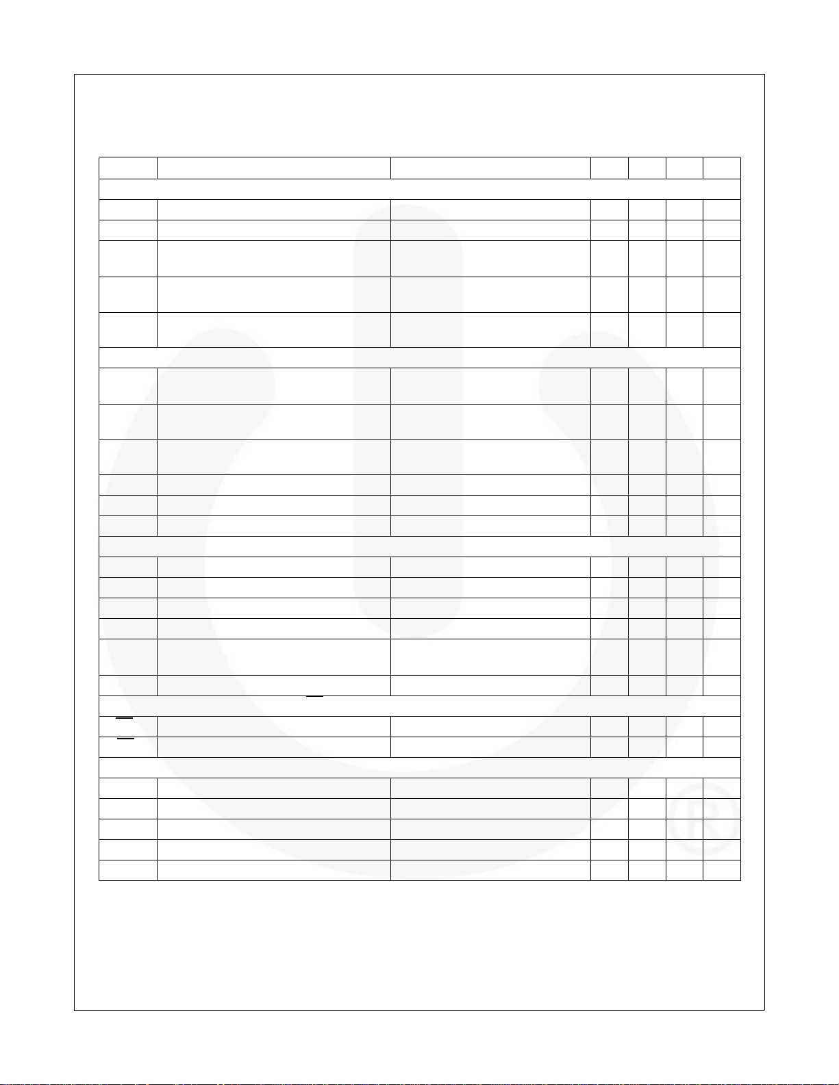
Electrical Characteristics
V
BIAS (VDD
The VO and IO parameters are referenced to VS and GND and are applicable to the respective outputs HO and LO.
Symbol Characteristics Condition Min. Typ. Max. Unit
LOW SIDE POWER SUPPLY SECTION
I
I
V
DDUV+
V
DDUV-
V
DDHYS
BOOTSTRAPPED POWER SUPPLY SECTION
V
BSUV+
V
BSUV-
V
BSHYS
I
I
GATE DRIVER OUTPUT SECTION
V
V
V
SL
SHUTDOWN CONTROL SECTION (SD
SD
SD
LOGIC INPUT SECTION (HIN, LIN)
V
INHYS
, VBS) = 15.0V, TA = 25C, unless otherwise specified. The VIN and IIN parameters are referenced to GND.
QDD
PDD
Quiescent VDD supply current V
Operating VDD supply current f
VDD supply under-voltage positive going
threshold
VDD supply under-voltage negative going
threshold
VDD supply under-voltage lockout
hysteresis
VBS supply under-voltage positive going
threshold
VBS supply under-voltage negative going
threshold
VBS supply under-voltage lockout
hysteresis
I
QBS
PBS
I
I
V
Offset supply leakage current VB=VS=600V 10 A
LK
Quiescent VBS supply current V
Operating VBS supply current f
High-level output voltage, V
OH
Low-level output voltage, V
OL
Output HIGH short-circuit pulse current VO=0V, VIN=5V with PW<10µs 200 250 mA
O+
Output LOW short-circuit pulsed current VO=15V, VIN=0V with PW<10µs 420 500 mA
O-
Allowable negative VS pin voltage for IN
S
signal propagation to H
-GND VSL-GND/GND-V
BIAS-VO
O
O
voltage endurability -7.0 7.0 V
SL
=0V or 5V 600 800 A
LIN
=20kHz, rms value 9 50 1300 A
LIN
V
=Sweep 10.9 11.9 12.9 V
DD
=Sweep 10.4 11.4 12.4 V
V
DD
=Sweep 0.5 V
V
DD
V
=Sweep 10.6 11.5 12.4 V
BS
=Sweep 10.1 11.0 11.9 V
V
BS
=Sweep 0.5 V
V
BS
=0V or 5V 50 90 A
HIN
=20kHz, rms value 400 600 A
HIN
IO=0mA (No Load) 100 mV
IO=0mA (No Load) 100 mV
-9.8 -7.0 V
)
+ Shutdown "1" input voltage 1.2 V
- Shutdown "0" input voltage 2.5 V
V
V
Logic "1" input voltage 2.5 V
IH
Logic "0" input voltage 1.2 V
IL
Logic input hysteresis voltage 0.5 V
I
I
IN+
Logic "1" input bias current VIN=5V 101520A
Logic "0" input bias current VIN=0V 2.0 A
IN-
FAN7384 — Half-Bridge Gate-Drive IC
© 2006 Fairchild Semiconductor Corporation www.fairchildsemi.com
FAN7384 Rev. 1.0.8 6
Page 7
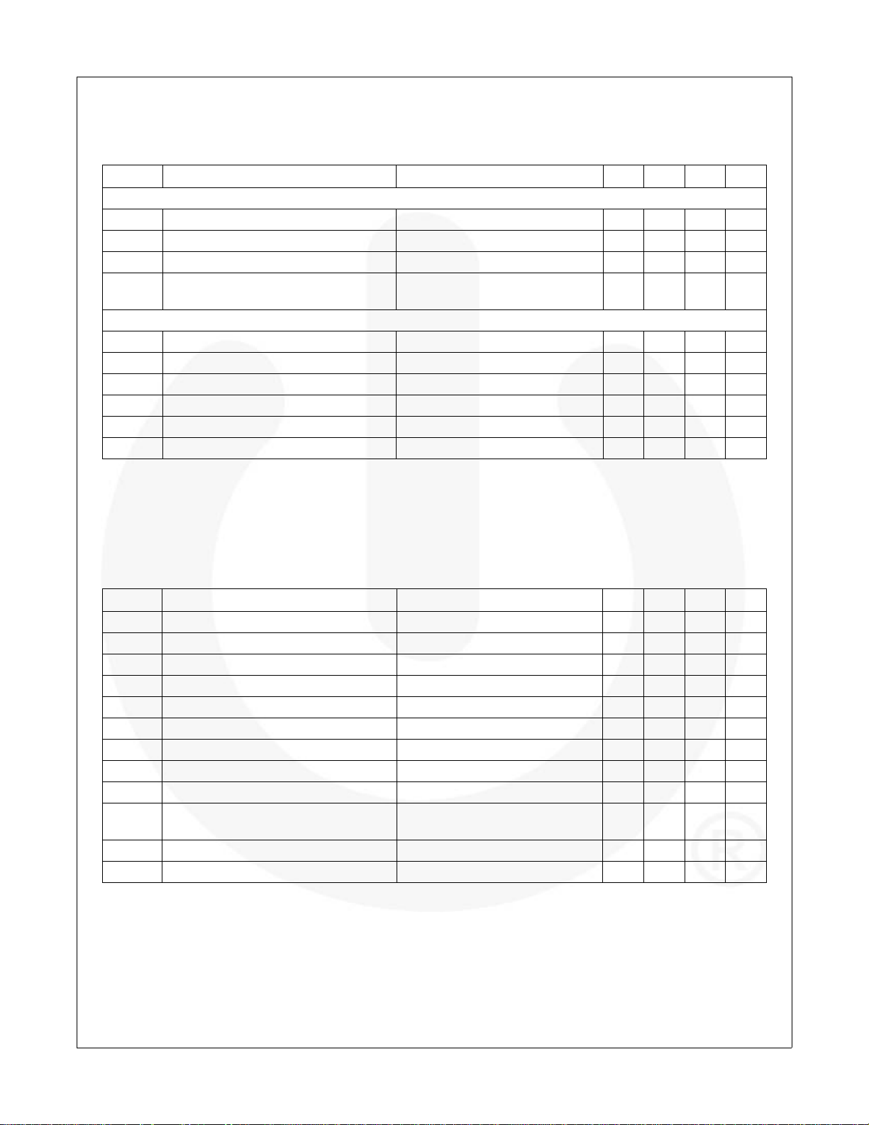
Electrical Characteristics (Continued)
V
BIAS (VDD
The V
Symbol Characteristics Condition Min. Typ. Max. Unit
SHORT-CIRCUIT PROTECTION
V
CSCREF
I
CSCIN
I
SOFT
-V
FAULT DETECTION SECTION
V
V
V
FINHYS
V
V
Note:
5. These parameters guaranteed by design.
, VBS) = 15.0V, TA = 25C, unless otherwise specified. The VIN and IIN parameters are referenced to GND.
and IO parameters are referenced to GND and VS is applicable to HO and LO.
O
Short-circuit detector reference voltage 0.47 0.50 0.53 V
Short-circuit input current V
CSCIN
=1V, R
=100K 51015A
CSCIN
Soft turn-off source current VDD=15V 5 10 15 mA
CSC
FINH
FINL
FOH
FOL
t
FO
Negative CSC pin immunity
(5)
Fault input high level voltage 2.5 V
Fault input low level voltage 1.2 V
Fault input hysteresis voltage
(5)
Fault output high level voltage V
Fault output low level voltage V
Fault output pulse width V
Voltage on CSC pin up to -12V,
Time<2s
0.5 V
=0V, R
CSC
CSC
CSCIN
PULL-UP
=1V, IFO=2mA 0.8 V
=1V 60 100 µs
=4.7K 4.7 V
-20 V
FAN7384 — Half-Bridge Gate-Drive IC
Dynamic Electrical Characteristics
TA=25C, V
BIAS (VDD
Symbol Parameter Conditions Min. Typ. Max. Unit
t
t
MT Delay matching 50 ns
DT Dead-time 80 120 170 ns
t
UVFLT
t
CSCFLT
t
CSCFO
t
CSCLO
t
SDFO
t
SDOFF
Note:
5. These parameters guaranteed by design.
Turn-on propagation delay VS=0V 180 260 ns
on
Turn-off propagation delay VS=0V or 600V
off
Turn-on rise time 50 100 ns
t
r
Turn-off fall time 30 80 ns
t
f
Under-voltage filtering time
CSC pin filtering time
Time from CSC triggering to FO
Time from CSC triggering to low-side
gate output
Shutdown to FO propagation delay
Shutdown to HIGH/LOW-side gate off
, VBS) = 15.0V, VS = GND, C
(5)
(5)
(5)
(5)
(5)
= 1000pF unless otherwise specified.
Load
(5)
From V
=1V to starting gate
CSC
turn-off
(5)
170 240 ns
16 µs
300 ns
350 ns
600 ns
60
100
ns
ns
© 2006 Fairchild Semiconductor Corporation www.fairchildsemi.com
FAN7384 Rev. 1.0.8 7
Page 8
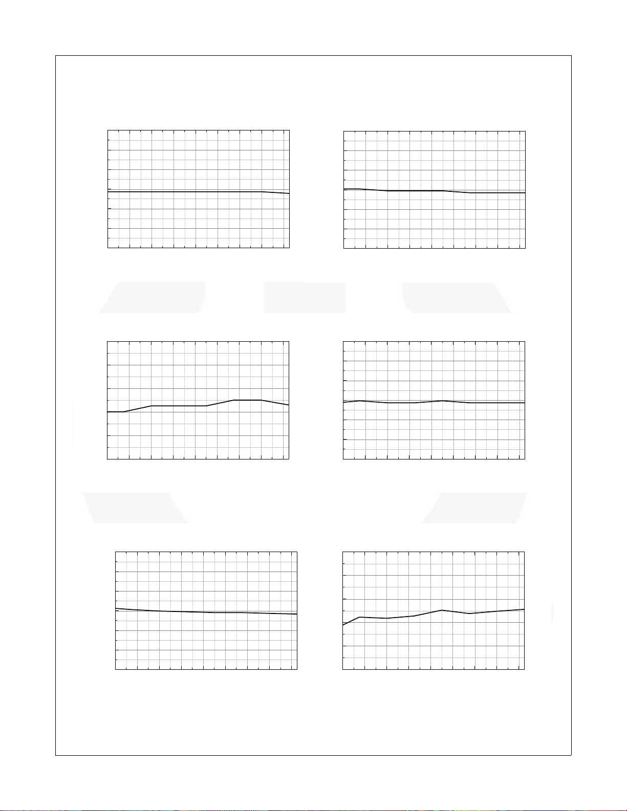
Typical Characteristics
-40 -20 0 20 40 60 80 100 120
10.5
11.0
11.5
12.0
12.5
13.0
13.5
V
DDUV
+ [V]
Temperature [°C]
-40 -20 0 20 40 60 80 100 120
10.0
10.5
11.0
11.5
12.0
12.5
13.0
V
DDUV
- [V]
Temperature [°C]
-40-200 20406080100120
0.0
0.2
0.4
0.6
0.8
1.0
V
DDHYS
[V]
Temperature [°C]
-40 -20 0 20 40 60 80 100 120
10.0
10.5
11.0
11.5
12.0
12.5
13.0
V
BSUV
+ [V]
Temperature [°C]
-40 -20 0 20 40 60 80 100 120
9.5
10.0
10.5
11.0
11.5
12.0
12.5
V
BSUV
- [V]
Temperature [°C]
-40-200 20406080100120
0.0
0.2
0.4
0.6
0.8
1.0
V
BSHYS
[V]
Temperature [°C]
Figure 5. VDD UVLO (+) vs. Temperature Figure 6. VDD UVLO (-) vs. Temperature
FAN7384 — Half-Bridge Gate-Drive IC
Figure 7. V
© 2006 Fairchild Semiconductor Corporation www.fairchildsemi.com
FAN7384 Rev. 1.0.8 8
Figure 9. V
UVLO Hysteresis vs. Temperature Figure 8. VBS UVLO (+) vs. Temperature
DD
UVLO (-) vs. Temperature Figure 10. VBS UVLO Hysteresis vs. Temperature
BS
Page 9
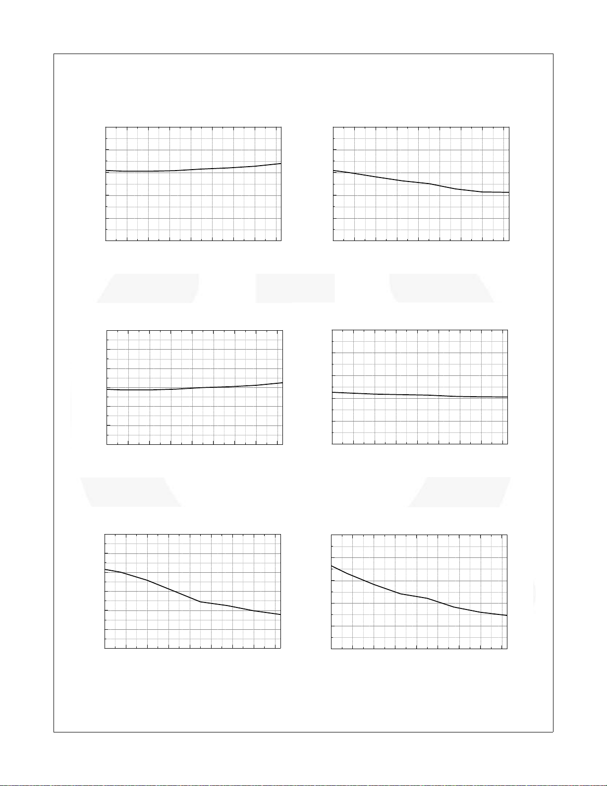
Typical Characteristics (Continued)
-40 -20 0 20 40 60 80 100 120
0
200
400
600
800
1000
I
QDD
[A]
Temperature [°C]
-40-200 20406080100120
0
20
40
60
80
100
I
QBS
[A]
Temperature [°C]
-40 -20 0 20 40 60 80 100 120
400
600
800
1000
1200
1400
1600
I
PDD
[A]
Temperature [°C]
-40-200 20406080100120
0
200
400
600
800
1000
I
PBS
[A]
Temperature [°C]
-40-200 20406080100120
0
5
10
15
20
25
30
I
IN
+ [A]
Temperature [°C]
-40 -20 0 20 40 60 80 100 120
0
4
8
12
16
20
I
CSCIN
[A]
Temperature [°C]
Figure 11. VDD Quiescent Current vs. Temperature Figure 12. VBS Quiescent Current vs. Temperature
FAN7384 — Half-Bridge Gate-Drive IC
Figure 13. V
© 2006 Fairchild Semiconductor Corporation www.fairchildsemi.com
FAN7384 Rev. 1.0.8 9
Figure 15. Logic Input Current vs. Temperature Figure 16. I
Operating Current vs. Temperature Figure 14. VBS Operating Current vs. Temperature
DD
vs. Temperature
CSCIN
Page 10

Typical Characteristics (Continued)
-40 -20 0 20 40 60 80 100 120
0
5
10
15
20
I
SOFT
[mA]
Temperature [°C]
-40-200 20406080100120
0
20
40
60
80
100
120
t
r
[nsec]
Temperature [°C]
-40-200 20406080100120
0
20
40
60
80
100
t
f
[nsec]
Temperature [°C]
-40-200 20406080100120
0
50
100
150
200
250
300
t
on
[nsec]
Temperature [°C]
-40-200 20406080100120
0
50
100
150
200
250
300
t
off
[nsec]
Temperature [°C]
-40-200 20406080100120
0.0
0.5
1.0
1.5
2.0
2.5
3.0
V
IH
[V]
Temperature [°C]
FAN7384 — Half-Bridge Gate-Drive IC
Figure 17. I
vs. Temperature Figure 18. Turn-on Rising Time vs. Temperature
SOFT
Figure 19. Turn-off Falling Time vs. Temperature Figure 20. Turn-on Delay Time vs. Temperature
© 2006 Fairchild Semiconductor Corporation www.fairchildsemi.com
FAN7384 Rev. 1.0.8 10
Figure 21. Turn-off Delay Time vs. Temperature Figure 22. Logic Input High Voltage vs. Temperature
Page 11
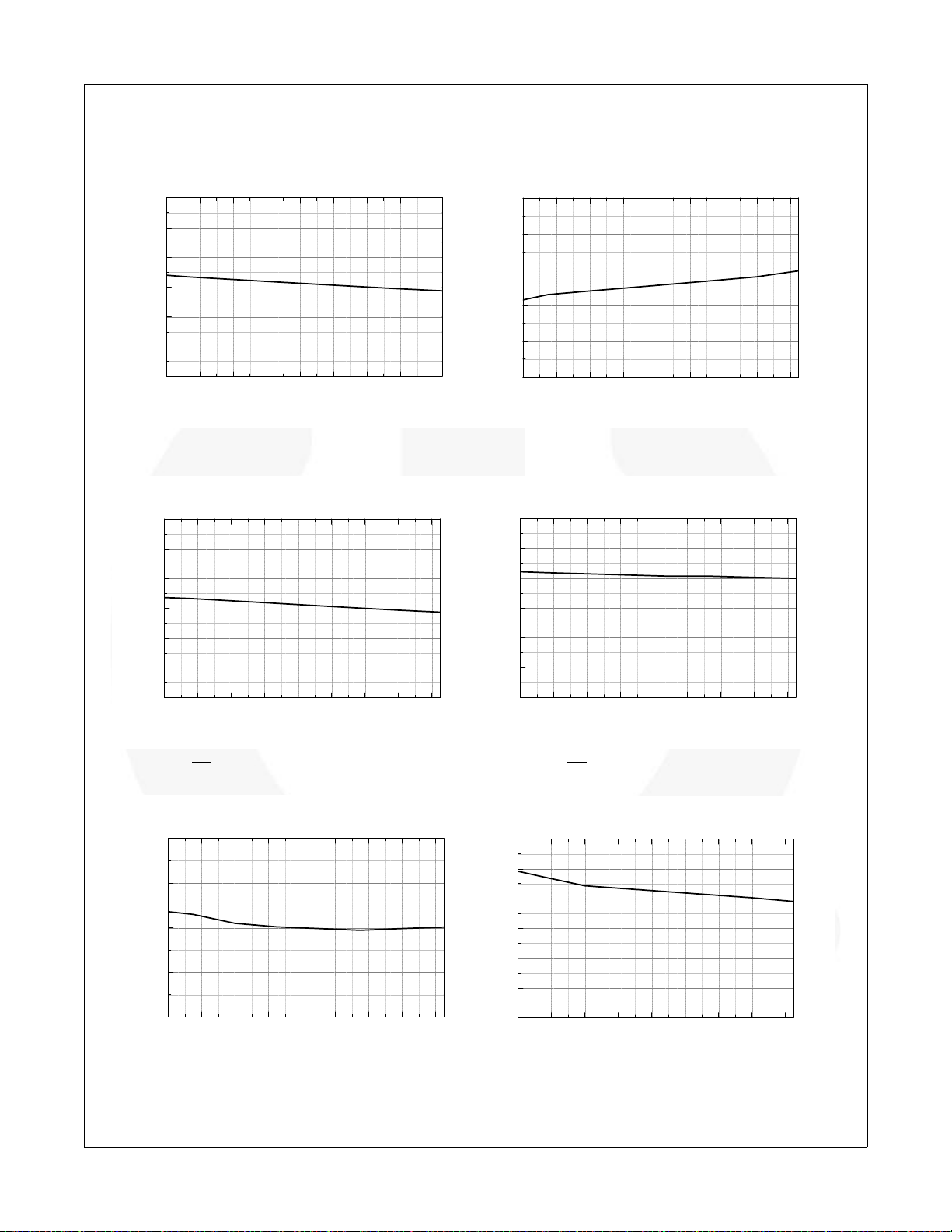
Typical Characteristics (Continued)
-40-200 20406080100120
0.0
0.5
1.0
1.5
2.0
2.5
3.0
V
IL
[V]
Temperature [°C]
-40-200 20406080100120
0.0
0.2
0.4
0.6
0.8
1.0
V
INHYS
[V]
Temperature [°C]
-40-200 20406080100120
0.0
0.5
1.0
1.5
2.0
2.5
3.0
SD
BAR
+ [V]
Temperature [°C]
-40-200 20406080100120
0.0
0.5
1.0
1.5
2.0
2.5
3.0
SD
BAR
- [V]
Temperature [°C]
-40 -20 0 20 40 60 80 100 120
0.40
0.45
0.50
0.55
0.60
V
CSCREF
[V]
Temperature [°C]
-40-200 20406080100120
0.0
0.4
0.8
1.2
1.6
2.0
2.4
V
FINH
[V]
Temperature [°C]
Figure 23. Logic Input Low Voltage vs. Temperature Figure 24. Logic Input Hysteresis vs. Temperature
FAN7384 — Half-Bridge Gate-Drive IC
Figure 25. SD
© 2006 Fairchild Semiconductor Corporation www.fairchildsemi.com
FAN7384 Rev. 1.0.8 11
Positive Threshold vs. Temperature F igure 26. SD Negative Threshold vs. Temperature
Figure 27. V
CSCREF
vs. Temperature Figure 28. Fault Input High Voltage vs. Temperature
Page 12
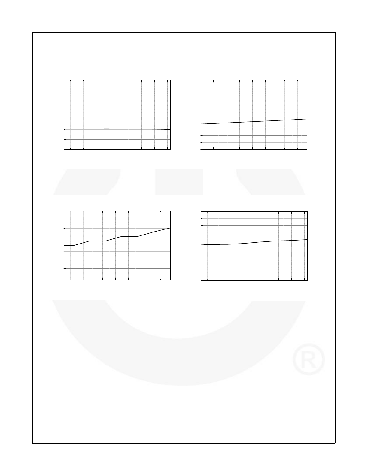
Typical Characteristics (Continued)
-40 -20 0 20 40 60 80 100 120
4.8
5.2
5.6
6.0
V
FOH
[V]
Temperature [°C]
-40-200 20406080100120
0.0
0.2
0.4
0.6
0.8
1.0
V
FOL
[V]
Temperature [°C]
-40 -20 0 20 40 60 80 100 120
-13
-12
-11
-10
-9
-8
-7
V
S
[V]
Temperature [°C]
-40-200 20406080100120
0
40
80
120
160
200
DT [nsec]
Temperature [°C]
FAN7384 — Half-Bridge Gate-Drive IC
Figure 29. Fault Output High Voltage vs.
Temperature
Figure 31. Allowable Negative V
Voltage for Signal
S
Propagation to High Side vs. Temperature
Figure 30. Fault Output Low Voltage vs. Temperature
Figure 32. Dead Time vs. Temperature
© 2006 Fairchild Semiconductor Corporation www.fairchildsemi.com
FAN7384 Rev. 1.0.8 12
Page 13

Switching Time Definitions
LIN
V
DD
LO
FO
SD
t
UVFLT
t
FO
t
FO
Under-Voltage
Detection Point
Shutdown
Enable Point
Short-Circuit
Detection Point
UVLO-
Soft-Off
Operating
Soft-Off
Operating
Shutdown
Disable Point
Shutdown
Disable Skip
0.5V
t
CSCLO
t
CSCFO
t
CSCLO
t
CSCFO
Low-Side Output
Disable
Low-Side Output
Disable
V
CSC
FAN7384 Rev.03
The overall switching timing waveforms definition of FAN7384 as shown Figure 33.
FAN7384 — Half-Bridge Gate-Drive IC
Figure 33. Switching Timing Waveforms Definition
© 2006 Fairchild Semiconductor Corporation www.fairchildsemi.com
FAN7384 Rev. 1.0.8 13
Page 14

Typical Application Information
t
UVFLT
t
CSCLO
UVLO+
90%
LIN
V
DD
LO
FO
UVLO-
t
FO
FAN7384 Rev.01
t
CSCFO
t
1
t
2t3
After DT
HIN/LIN
LIN/HIN
LO/HO
HO/LO
After DT
Shoot-Through Prevent
FAN7384 Rev.01
HIN/LIN
LIN/HIN
LO/HO
HO/LO
After DT
Shoot-Through Prevent
FAN7384 Rev.01
(1)
CSCREF
CS
CS
V
R
t
FO
Short-Circuit
Detection Point
Soft-Off
Operating
t
CSCLO
t
CSCFO
Low-SideOutput
Disable
0.5V
LIN
LO
FO
V
CSC
FAN7384 Rev.03
1. Protection Function
1.1 Under-Voltage Lockout (UVLO)
The high- and low-side drivers include under-voltage
lockout (UVLO) protection circuitry that monitors the
supply voltage (VDD) and bootstrap capacitor voltage
) independently. It can be designed to prevent
(V
BS
malfunction when V
specified threshold voltage. Moreover, the UVLO
hysteresis prevents chattering during power supply
transitions. If the supply voltage (V
under-voltage condition over under-voltage filtering times
(typically 16µs), the fault and soft-off circuits are
activated, as shown Figure 34.
Figure 34. Waveforms for Under-Voltage Lockout
and VBS are lower than the
DD
) maintains an
DD
Figure 36. Waveforms for Shoot-Through Prevention
1.3 Over-Current Protection Function
The FAN7384 has over-current detection circuitry that
monitors the current-by-current sensing resistor connected from the low-side switch source (V
) to ground.
SL
It is a built-in time-filler from the over-current event to
prevent malfunction from a noise source, such as leading-edge pulse in inductive load application, as shown
Figure 37.
The sensing current is calculated as follows:
I[A]
FAN7384 — Half-Bridge Gate-Drive IC
1.2 Shoot-Through Prevention Function
The FAN7384 has a shoot-through prevention circuitry
that monitors the high- and low-side inputs. It can be
designed to prevent outputs of high- and low-side turning
on at same time, as shown Figure 35 and 36.
Figure 35. Wav eforms for Shoot-Throu gh Prevention
© 2006 Fairchild Semiconductor Corporation www.fairchildsemi.com
FAN7384 Rev. 1.0.8 14
where,
V
: Reference voltage of current sense
CSCREF
comparator
RCS: Current sensing resistor
Figure 37. Waveforms for Short-Circuit Protection
Page 15

FAN7384 — Half-Bridge Gate-Drive IC
2. Layout Considerations
For optimum performance, considerations must be taken
during printed circuit board (PCB) layout.
2.1 Supply Capacitors
If the output stages are able to quickly turn on a switching device with a high value of current, the suppl y cap a citors must be placed as close as possible to the device
pins (V
VS for the floating supply) to minimize parasitic inductance and resistance.
and GND for the ground-tied supply, VB and
DD
2.2 Gate-Drive Loop
Current loops behave like antennae, able to receive and
transmit noise. To reduce the noise coupling/emission
and improve the power switch turn-on and off performance, gate-drive loops must be reduced as much as
possible.
2.3 Ground Plane
To minimize noise coupling, the ground plane should not
be placed under or near the high-voltage floating side.
© 2006 Fairchild Semiconductor Corporation www.fairchildsemi.com
FAN7384 Rev. 1.0.8 15
Page 16

Package Dimensions
FAN7384 — Half-Bridge Gate-Drive IC
Figure 38. 14-Lead, Small Outline Integrated Circuit (SOIC), Non-JEDEC, .150 Inch Narrow Body, 225SOP
Package drawings are provided as a service to customers considering Fairchild co mponents. Drawings may change in any manner
without notice. Please note the revision and/or date on the drawing and contact a Fairchild Semiconductor r epresentative to ver ify or
obtain the most recent revision. Package specifications do not expand the terms of Fairchild’s worldwide terms and conditions,
specifically the warranty therein, which covers Fairchild products.
Always visit Fairchild Semiconductor’s online packaging area for the most recent package drawings:
http://www.fairchildsemi.com/packaging/
© 2006 Fairchild Semiconductor Corporation www.fairchildsemi.com
FAN7384 Rev. 1.0.8 16
Page 17

FAN7384 — Half-Bridge Gate-Drive IC
© 2006 Fairchild Semiconductor Corporation www.fairchildsemi.com
FAN7384 Rev. 1.0.8 17
 Loading...