

Page 1
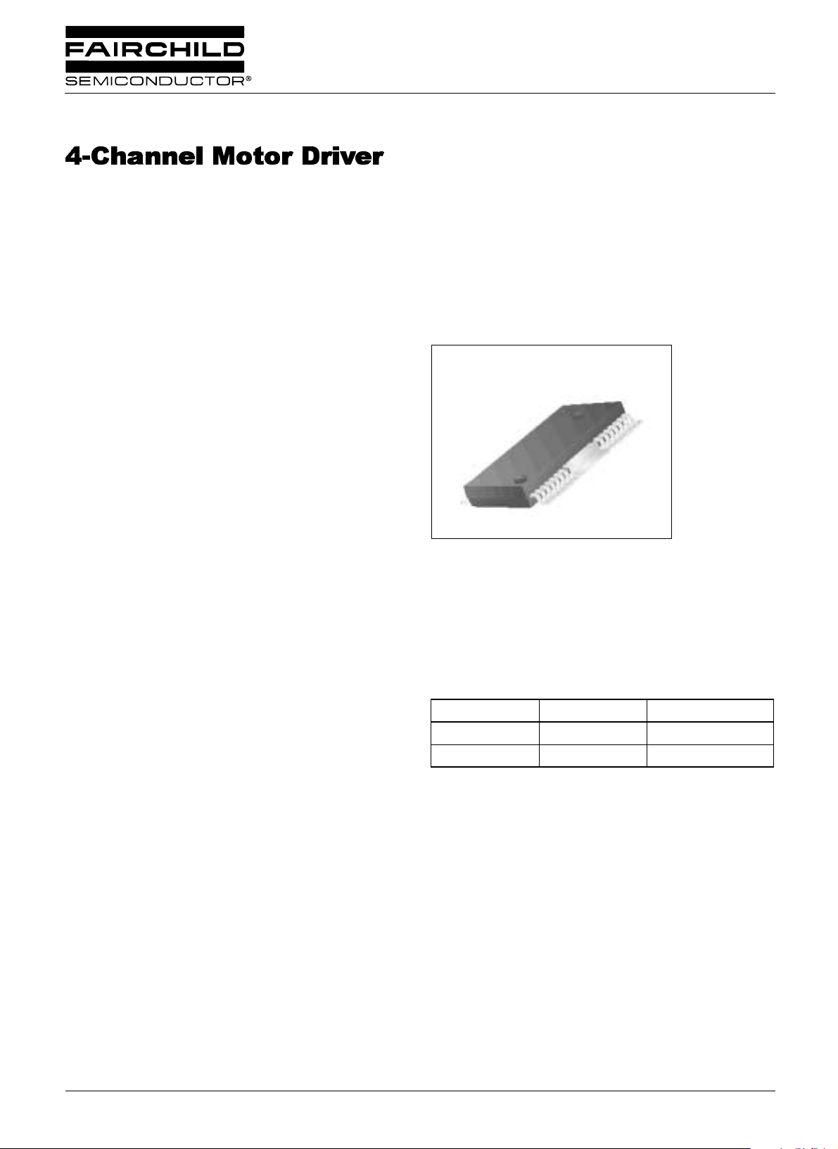
FAN8024BD
4-Channel Motor Driver
www.fairchildsemi.com
Features
• 2-Channel BTL driver with current feedback
• 2-C hann el BT L DC motor d r iver
• Built-in thermal shutdown circuit
• Built-in mute circuit
• Operating supply voltage: 4.5~13.2V
Description
The FAN8024BD is a monolithic IC, suitable for 2-ch BTL
DC motor drivers and 2-ch motor driv ers with current
feedback which drive the focus and tracking actuators of a
CD- media system.
28-SSOPH-375
Typical Applications
• Compac t disk RO M (CD- ROM)
• Compact disk RW (C D - RW)
• Digital video disk ROM (DVD-ROM)
• Digital video disk RAM (DVD-RAM)
• Digital video disk player (DVDP)
• Other compact disk media
Ordering Information
Device Package Operating Temp.
FAN8024BD 28-SSOPH-375 -25 °C ~ 85 °C
FAN8024BDTF 28-SSOPH-375 -25 °C ~ 85 °C
Rev . 1.0.1
©2002 Fairchild Semiconductor Corporation
Page 2
FAN8024BD
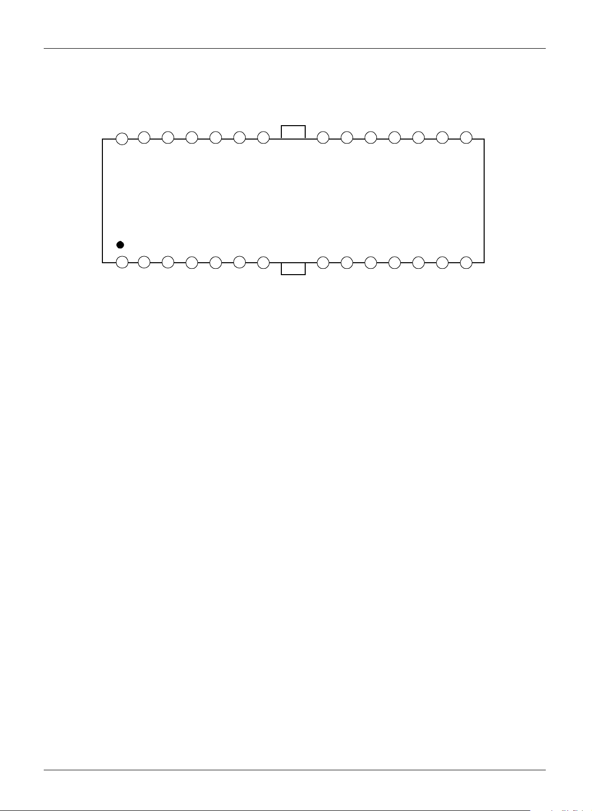
Pin Ass ign m e n ts
STBY
REF
27 26 25 24 23 22 21 20 19 18 17 16 15
28
(GND)
FIN
IN4
CAP4.1
CAP4.2
IN3
VCCGND
PVCC2
FB4
PGND2
DO3−DO3+
DO4−DO4+
FAN8024BD
123
IN1
CAP1.2
CAP1.1
45
IN2.1
IN2.2
7
6
FIN
FB1
OUT2
(GND)
89
VCC
PVCC1
10 11
PGND1
−
DO2
12
DO2+
13 14
−
DO1
DO1+
2
Page 3

Pin Defi ni ti o n s
Pin Number Pin Name I/O Pin Function Description
1 IN1 I CH1 input 2 CAP1.1 - Connection with capacitor 3 CAP1.2 - for CH1 4 IN2.1 I OP-AMP CH2 input(+) 5 IN2.2 I OP-AMP CH2 input(-) 6 OUT2 O OP-AMP CH2 output 7 FB1 I Feedback for CH1 8 VCC - Signal Vcc
9 PVCC1 - Power Supply 1 10 PGND1 - P ower Groun d 1 11 DO2 12 DO2 + O Drive2 Out put (+ ) 13 DO1 14 DO1 + O Drive1 Out put (+ ) 15 DO4 + O Drive4 Out put (+ ) 16 DO4 17 DO3 + O Drive3 Out put (+ ) 18 DO3 19 PGND2 - P ower Groun d 2 20 FB4 - Feedback for CH4 21 PVCC2 - Power Supply 2 22 VCCGND - Vcc ground 23 IN3 I CH3 input 24 CAP4.2 - Connection with capacitor 25 CAP4.1 - for CH4 26 IN4 I CH4 input 27 REF I B ias voltage input 28 STBY I Stand-by input
−
−
−
−
O Drive2 Output (-)
O Drive1 Output (-)
O Drive4 Output (-)
O Drive3 Output (-)
FAN8024BD
3
Page 4
FAN8024BD
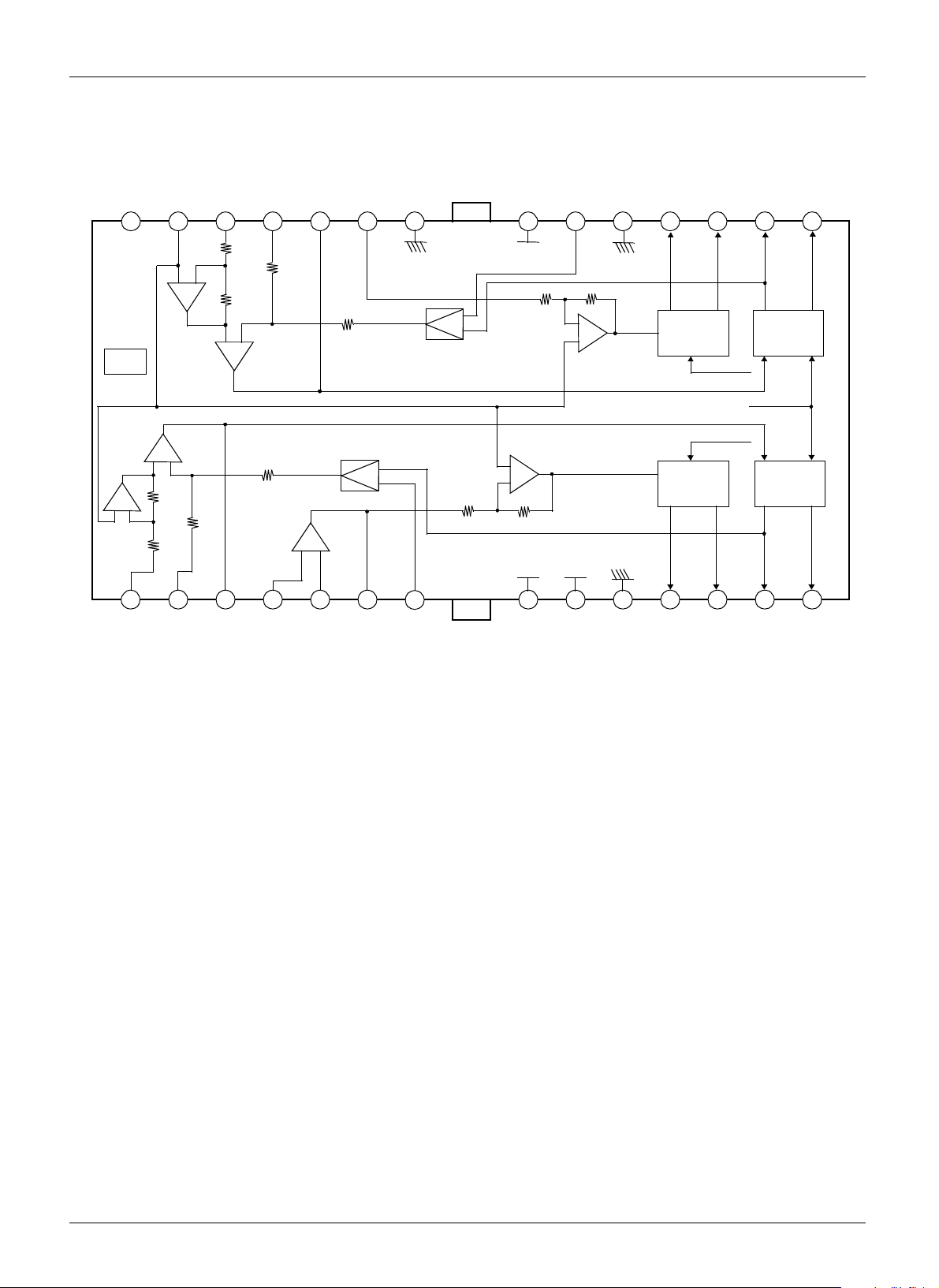
Internal Bl oc k Diag r am
STBY
REF
28 27 26 25 24 23 22 21 20 19 18 17 16 15
+
S
T
D
-
+
K
0
-
+
2
K
0
1
12345
IN1
CAP1.1
IN4
-
+
K
5
.
7
CAP1.2
CAP4.1
K
0
1
K
0
2
-
7
.
5
K
IN2.1
CAP4.2
IN3
K
5
.
7
7
5
.
K
X
2
-
+
67
IN2.2
OUT2
VCCGND
X
2
FB1
GND
1
0
GND
PVCC2
V
P
C
C
1
+
-
K
2
5
K
V
C
C
89
VCC
FB4
PGND2
2
1
5
0
K
K
-
+
1
C
C
V
P
10 11
PGND1
PVCC1
DO3−DO3+
Loading
Driver
Sled
Driver
−
DO2
12
P
P
V
C
V
C
V
DO2+
DO4−DO4+
Actuator
Driver
C
1
2
C
C
C
Actuator
Driver
13 14
−
DO1
DO1+
4
Page 5
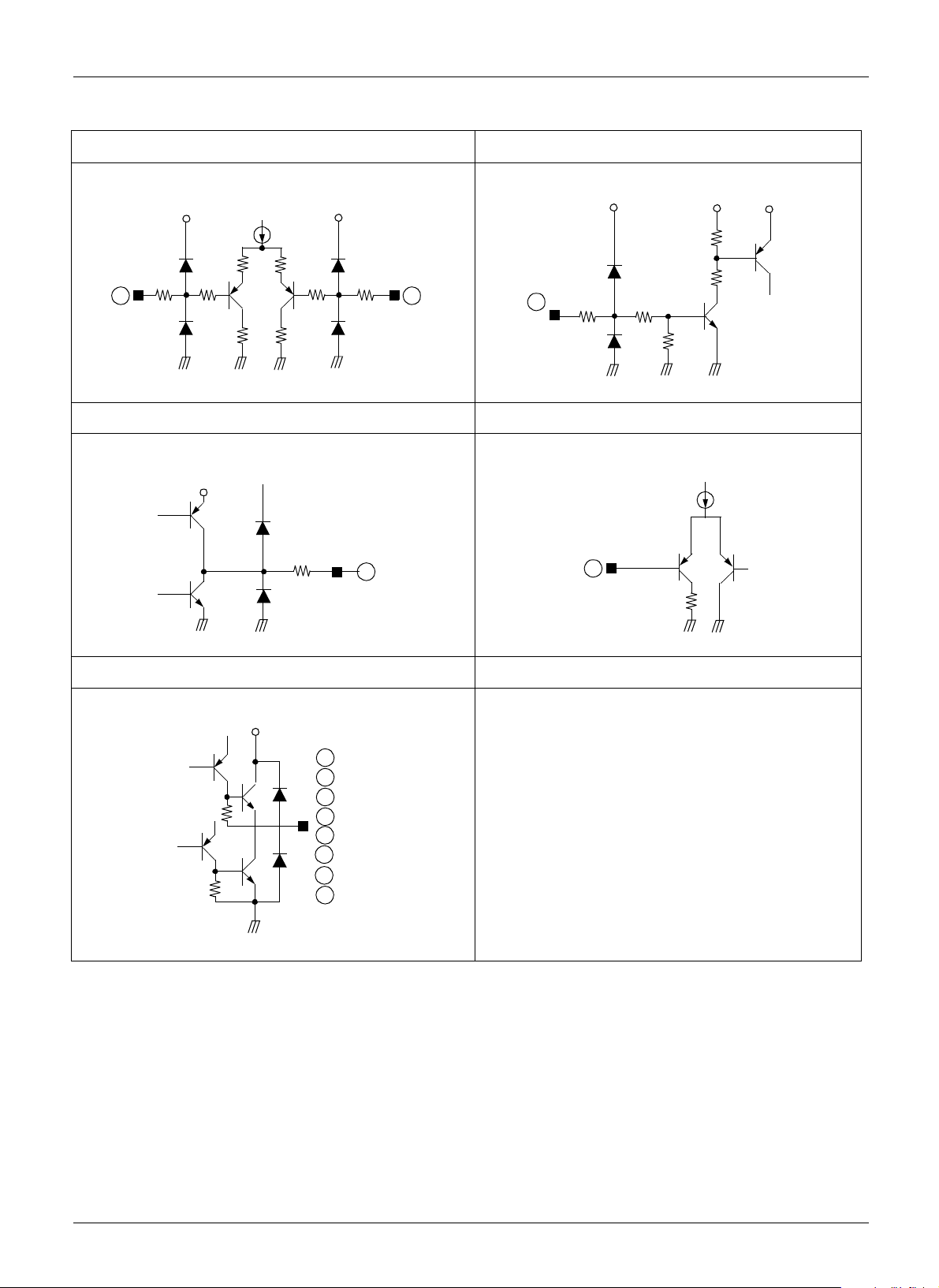
Equivalent Circuits
ERROR AMP INPUT STAND-BY INPUT
FAN8024BD
3KΩ
1KΩ
3KΩ
2KΩ2KΩ
1KΩ
54
28
50Ω
ERROR AMP OUTPUT SIGNAL REFERENCE INPUT
50Ω
6
27
50ΚΩ
POWER AMP OUTPUT
11
12
13
14
15
16
17
18
5
Page 6
FAN8024BD
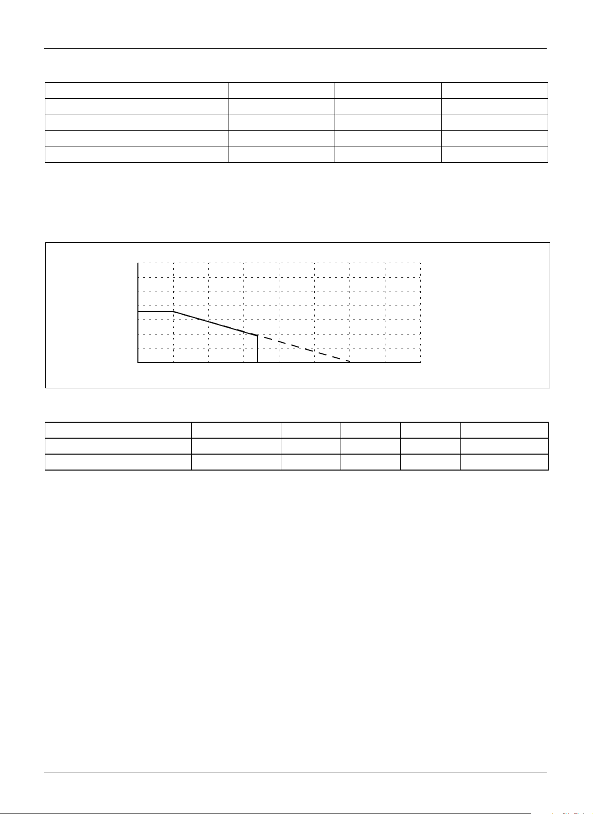
Absolute Maximum Ratings (Ta = 25°C)
Parameter Symbol Value Unit
Maximum supply voltage V
Power dissipation P
Operating temperature range T
Storage temperature range T
NOTE:
1. When mounted on a 50mm × 50mm × 1mm PCB (Phenolic resin material).
2. Power dissipation is reduced by -13.6mW/°C above Ta = 25°C
3. Should not exeed Pd(Po wer di ssipation) and SOA(Safe operating area).
CCmax
D
OPR
STG
15 V
note
1.7
-25 ~ +85 °C
-55 ~ +150 °C
Power Dissipation Curve
Pd [mW]
3,000
2,000
W
1,000
0
0
SOA
85
Recommended Operating Conditions (Ta = 25°C)
Parameter Symbol Min. Typ. Max. Unit
Supply Voltage V
Supply Voltage PV
CC1,PVCC2
CC
4.5 - 13.2 V
-VCC-V
175150125100755025
Ambient Temperature, Ta [°C]
6
Page 7
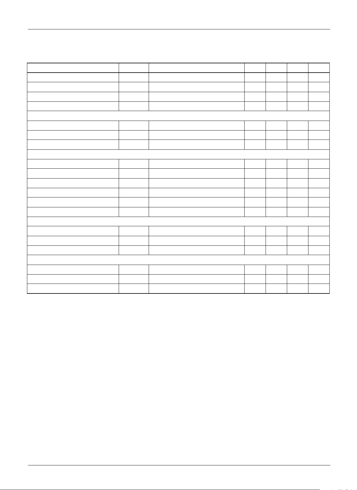
Electrical Characteristics
(Unless otherwise specified, Ta = 25 °C, VCC = 12V, PVCC1,2 = 5V)
Parameter Symbol Conditions Min. Typ. Max. Unit
Quiescent Current1 I
Quiescent Current1 I
Stand-by On Voltage V
Stand-by Off Voltage V
ACTUATOR DRIVE CIRCUIT
Output Offset Current I
OO1,4
Maximum Output Voltage1 V
Transconductance G
PRE OP
AMP (SLED DRIVER)
Common mode Input Range* V
Inpu t B i a s Curre n t I
Low Level Output Voltage V
High Level Output Voltage V
Output Source Current I
SOURCE
Output Sink Current I
SLED DRIVE CIRCUIT
Output Offset voltage2 V
Maximum Output Voltage2 V
Closed loop Voltage Gain1 G
Loading DRIVE CIRCUIT
Output Offset Voltage1 V
Maximum Output Voltage 3 V
Closed loop Voltage Gain 2 G
CC1
CC2
STon
SToff
OM1,4
M1,4
OOM
B
OL
OH
SINK
OF2
OM2
VLO2
OF3
OM3
VLO3
Stand-by off - 18 27 mA
Stand-by on - - 0.5 mA
---0.5V
-2.0--V
--60+6mA
-3.64.0-V
VIN = 100mVp-p, f=1kHz 1.5 1.7 1.9 A/V
-0-11.0V
- -300 -30 - nA
--0.10.3V
- 10 10.9 - V
-14-mA
-510-mA
- -100 0 +100 mV
- 10.0 10.9 - V
VIN = 100mVp-p, f=1kHz 18.0 20.0 22.0 dB
--50050mV
-3.64.0-V
VIN = 100mVp-p, f=1KHz 13.5 15.5 17.5 dB
FAN8024BD
* : Guaranteed design value
7
Page 8

FAN8024BD
Application Information
1. Reference Input & Stand-by Function
• Reference input (PIN 27)
The applied voltage at the reference input pin must be between 0.8V and 6.5V, when V
• Stand-by input (PIN 28)
The following inpu t conditions must be satisfied for the normal st and-by function.
CC
=8.5V.
Stand-by input voltage Below 0.5V or OPEN
Stand-by function is activated so the bias block and the
power block are disabled
Stand-by input voltage Above 2.0V Normal operation
2. Protection Function
Thermal shutdo wn (TSD)
If the chip temperature rises above 175°C, the t herm al shutdown (TSD) circuit is activated and the output circuit is in the mute
state, that is off state. The TSD circuit has a temperature hysteresis of 25°C
3. Separation Of Power Supply
•PV
•PV
•V
(PIN 9)
CC1
PV
is the power supply for loading driver. The range is between 5V ~ 12V.
CC1
(PIN 21)
CC2
PV
is the power supply for actuat or drivers that include focus and tracking actua tors. The range is between 5V ~ 12V
CC2
(PIN 8)
CC
V
pin supplies power for sled driver and signal logic part. The voltage applied to VCC must be higher than PV
CC
and PV
at least 1V
CC2
cc1
8
Page 9
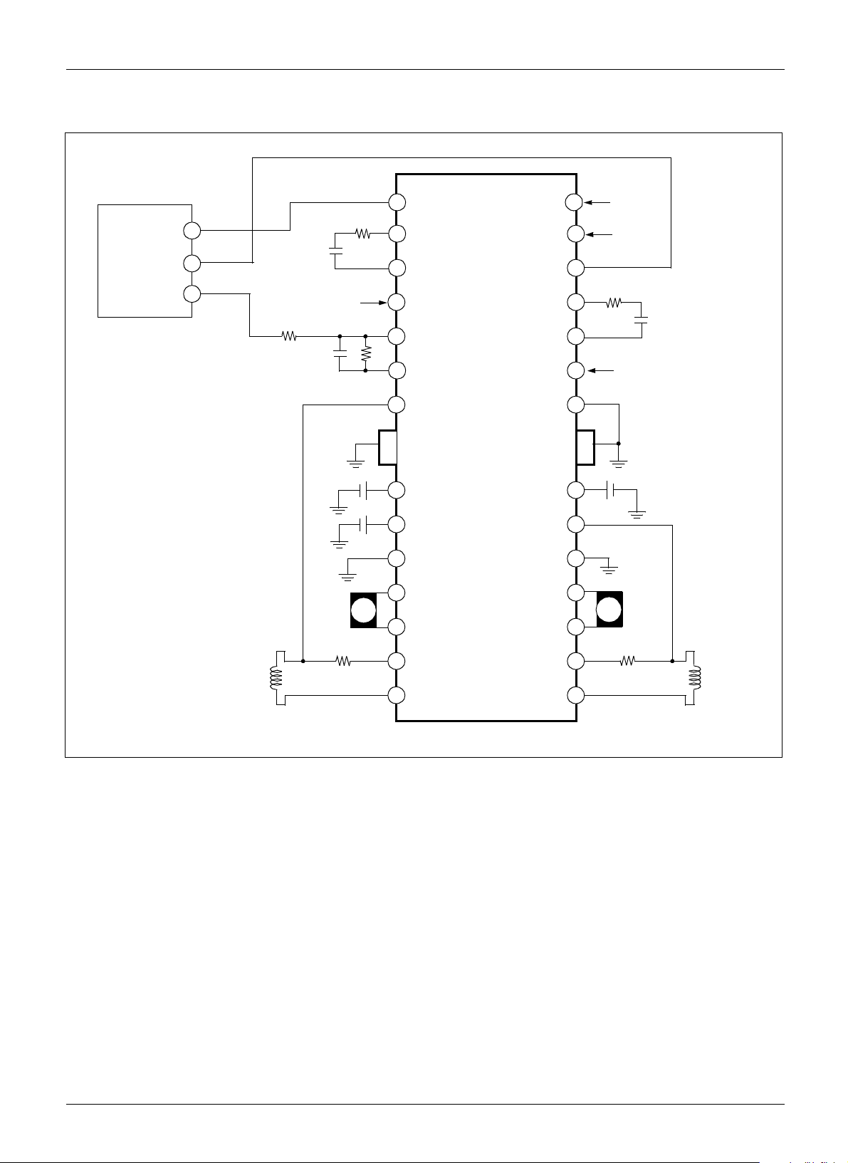
Typical Application Circuits
FAN8024BD
SERVO
AMP
FOCUS
TRACKING
SLED
SLED
MOTOR
REF
12V
5V or 12V
10
11
12
1
2
3
4
5
6
7
8
9
IN1
CAP1.1
CAP1.2
IN2.1
IN2.2
OUT2
FB1
VCC
PVCC1
PGND
DO2−
DO2+
FAN8024BD
STBY
REF
IN4
CAP4.1
CAP4.2
IN3
VCCGND
PVCC2
FB4
PGND
DO3−
DO3+
28
27
26
25
24
23
22
21
20
19
18
17
Stand by
REF
TRAY CONTROL IN
5V or 12V
TRAY
MOTOR
FOCUS
ACTUATOR
DO1−
R
D
13
14
DO1+
DO4−
DO4+
16
15
R
D
TRACKING
ACTUATOR
9
Page 10

FAN8024BD
DISCLAIMER
FAIRCHILD SEMICONDUCTOR RESERVES THE RIGHT TO MAKE CHANGES WITHOUT FURTHER NOTICE TO ANY
PRODUCTS HEREIN TO IMPROVE RELIABILITY, FUNCTION OR DESIGN. FAIRCHILD DOES NOT ASSUME ANY
LIABILITY ARISING OUT OF THE APPLICATION OR USE OF ANY PRODUCT OR CIRCUIT DESCRIBED HEREIN; NEITHER
DOES IT CONVEY ANY LICENSE UNDER ITS PATENT RIGHTS, NOR THE RIGHTS OF OTHERS.
LIFE SUPPORT POLICY
FAIRCHILD’S PRODUCTS ARE NOT AUTHORIZED FOR USE AS CRITICAL COMPONENTS IN LIFE SUPPORT DEVICES
OR SYSTEMS WITHOUT THE EXPRESS WRITTEN APPROVAL OF THE PRESIDENT OF FAIRCHILD SEMICONDUCTOR
CORPORATION. As used herein:
1. Life support devices or systems are devices or systems
which, (a) are inte nded for surgical implant into the body,
or (b) support or sustain life, and (c) whose fail ure to
perform when proper ly used in accordance with
2. A critical component in any component of a life support
device or system whose failure to perform can be
reasonably exp ected to c ause t he failure of the l ife suppo rt
device or system, or to aff ect its safety or effectiveness.
instruct ions for use provided in the labeling, can be
reasonably expected to result in a signi ficant injury of the
user.
www.fairchildsemi.com
10/1/02 0.0m 001
2002 Fairchild Semiconductor Corporation
Stock#DSxxxxxxxx
 Loading...