

Datasheet dsPIC33FJ64GP206, dsPIC33FJ64GP306, dsPIC33FJ64GP310, dsPIC33FJ64GP706, dsPIC33FJ64GP708 Datasheet
...
dsPIC33FJXXXGPX06/X08/X10
Data Sheet
High-Performance,
16-Bit Digital Signal Controllers
© 2009 Microchip Technology Inc. DS70286C
Note the following details of the code protection feature on Microchip devices:
• Microchip products meet the specification contained in their particular Microchip Data Sheet.
• Microchip believes that its family of products is one of the most secure families of its kind on the market today, when used in the
intended manner and under normal conditions.
• There are dishonest and possibly illegal methods used to breach the code protection feature. All of these methods, to our
knowledge, require using the Microchip products in a manner outside the operating specifications contained in Microchip’s Data
Sheets. Most likely, the person doing so is engaged in theft of intellectual property.
• Microchip is willing to work with the customer who is concerned about the integrity of their code.
• Neither Microchip nor any other semiconductor manufacturer can guarantee the security of their code. Code protection does not
mean that we are guaranteeing the product as “unbreakable.”
Code protection is constantly evolving. We at Microchip are committed to continuously improving the code protection features of our
products. Attempts to break Microchip’s code protection feature may be a violation of the Digital Millennium Copyright Act. If such acts
allow unauthorized access to your software or other copyrighted work, you may have a right to sue for relief under that Act.
Information contained in this publication regarding device
applications and the like is provided only for your convenience
and may be superseded by updates. It is your responsibility to
ensure that your application meets with your specifications.
MICROCHIP MAKES NO REPRESENTATIONS OR
WARRANTIES OF ANY KIND WHETHER EXPRESS OR
IMPLIED, WRITTEN OR ORAL, STATUTORY OR
OTHERWISE, RELATED TO THE INFORMATION,
INCLUDING BUT NOT LIMITED TO ITS CONDITION,
QUALITY, PERFORMANCE, MERCHANTABILITY OR
FITNESS FOR PURPOSE. Microchip disclaims all liability
arising from this information and its use. Use of Microchip
devices in life support and/or safety applications is entirely at
the buyer’s risk, and the buyer agrees to defend, indemnify and
hold harmless Microchip from any and all damages, claims,
suits, or expenses resulting from such use. No licenses are
conveyed, implicitly or otherwise, under any Microchip
intellectual property rights.
Trademarks
The Microchip name and logo, the Microchip logo, Accuron,
dsPIC, K
EELOQ, KEELOQ logo, MPLAB, PIC, PICmicro,
PICSTART, rfPIC, SmartShunt and UNI/O are registered
trademarks of Microchip Technology Incorporated in the
U.S.A. and other countries.
FilterLab, Linear Active Thermistor, MXDEV, MXLAB,
SEEVAL, SmartSensor and The Embedded Control Solutions
Company are registered trademarks of Microchip Technology
Incorporated in the U.S.A.
Analog-for-the-Digital Age, Application Maestro, CodeGuard,
dsPICDEM, dsPICDEM.net, dsPICworks, dsSPEAK, ECAN,
ECONOMONITOR, FanSense, In-Circuit Serial
Programming, ICSP, ICEPIC, Mindi, MiWi, MPASM, MPLAB
Certified logo, MPLIB, MPLINK, mTouch, nanoWatt XLP,
PICkit, PICDEM, PICDEM.net, PICtail, PIC
32
logo, PowerCal,
PowerInfo, PowerMate, PowerTool, REAL ICE, rfLAB, Select
Mode, Total Endurance, TSHARC, WiperLock and ZENA are
trademarks of Microchip Technology Incorporated in the
U.S.A. and other countries.
SQTP is a service mark of Microchip Technology Incorporated
in the U.S.A.
All other trademarks mentioned herein are property of their
respective companies.
© 2009, Microchip Technology Incorporated, Printed in the
U.S.A., All Rights Reserved.
Printed on recycled paper.
Microchip received ISO/TS-16949:2002 certification for its worldwide
headquarters, design and wafer fabrication facilities in Chandler and
Tempe, Arizona; Gresham, Oregon and design centers in California
and India. The Company’s quality system processes and procedures
are for its PIC
devices, Serial EEPROMs, microperipherals, nonvolatile memory and
analog products. In addition, Microchip’s quality system for the design
and manufacture of development systems is ISO 9001:2000 certified.
®
MCUs and dsPIC® DSCs, KEELOQ
®
code hopping
DS70286C-page ii © 2009 Microchip Technology Inc.

dsPIC33FJXXXGPX06/X08/X10
High-Performance, 16-Bit Digital Signal Controllers
Operating Range:
• Up to 40 MIPS operation (at 3.0-3.6V):
- Industrial temperature range
(-40°C to +85°C)
High-Performance DSC CPU:
• Modified Harvard architecture
• C compiler optimized instruction set
• 16-bit wide data path
• 24-bit wide instructions
• Linear program memory addressing up to 4M
instruction words
• Linear data memory addressing up to 64 Kbytes
• 83 base instructions: mostly 1 word/1 cycle
• Sixteen 16-bit General Purpose Registers
• Two 40-bit accumulators:
- With rounding and saturation options
• Flexible and powerful addressing modes:
- Indirect, Modulo and Bit-Reversed
• Software stack
• 16 x 16 fractional/integer multiply operations
• 32/16 and 16/16 divide operations
• Single-cycle multiply and accumulate:
- Accumulator write back for DSP operations
- Dual data fetch
• Up to ±16-bit shifts for up to 40-bit data
Direct Memory Access (DMA):
• 8-channel hardware DMA:
• 2 Kbytes dual ported DMA buffer area
(DMA RAM) to store data transferred via DMA:
- Allows data transfer between RAM and a
peripheral while CPU is executing code
(no cycle stealing)
• Most peripherals support DMA
Interrupt Controller:
• 5-cycle latency
• Up to 63 available interrupt sources
• Up to five external interrupts
• Seven programmable priority levels
• Five processor exceptions
Digital I/O:
• Up to 85 programmable digital I/O pins
• Wake-up/Interrupt-on-Change on up to 24 pins
• Output pins can drive from 3.0V to 3.6V
• All digital input pins are 5V tolerant
• 4 mA sink on all I/O pins
On-Chip Flash and SRAM:
• Flash program memory, up to 256 Kbytes
• Data SRAM, up to 30 Kbytes (includes 2 Kbytes
of DMA RAM):
System Management:
• Flexible clock options:
- External, crystal, resonator, internal RC
- Fully integrated PLL
- Extremely low jitter PLL
• Power-up Timer
• Oscillator Start-up Timer/Stabilizer
• Watchdog Timer with its own RC oscillator
• Fail-Safe Clock Monitor
• Reset by multiple sources
Power Management:
• On-chip 2.5V voltage regulator
• Switch between clock sources in real time
• Idle, Sleep and Doze modes with fast wake-up
Timers/Capture/Compare/PWM:
• Timer/Counters, up to nine 16-bit timers:
- Can pair up to make four 32-bit timers
- 1 timer runs as Real-Time Clock with external
32.768 kHz oscillator
- Programmable prescaler
• Input Capture (up to eight channels):
- Capture on up, down or both edges
- 16-bit capture input functions
- 4-deep FIFO on each capture
• Output Compare (up to eight channels):
- Single or Dual 16-Bit Compare mode
- 16-bit Glitchless PWM mode
© 2009 Microchip Technology Inc. DS70286C-page 1

dsPIC33FJXXXGPX06/X08/X10
Communication Modules:
• 3-wire SPI (up to two modules):
- Framing supports I/O interface to simple
codecs
- Supports 8-bit and 16-bit data
- Supports all serial clock formats and
sampling modes
2
C™ (up to two modules):
•I
- Full Multi-Master Slave mode support
- 7-bit and 10-bit addressing
- Bus collision detection and arbitration
- Integrated signal conditioning
- Slave address masking
• UART (up to two modules):
- Interrupt on address bit detect
- Interrupt on UART error
- Wake-up on Start bit from Sleep mode
- 4-character TX and RX FIFO buffers
- LIN bus support
®
-IrDA
- High-Speed Baud mode
- Hardware Flow Control with CTS and RTS
• Data Converter Interface (DCI) module:
- Codec interface
- Supports I
- Up to 16-bit data words, up to 16 words per
- 4-word deep TX and RX buffers
• Enhanced CAN (ECAN™ module) 2.0B active
(up to 2 modules):
- Up to eight transmit and up to 32 receive buffers
- 16 receive filters and three masks
- Loopback, Listen Only and Listen All
- Wake-up on CAN message
- Automatic processing of Remote
- FIFO mode using DMA
- DeviceNet™ addressing support
encoding and decoding in hardware
2
S and AC’97 protocols
frame
Messages modes for diagnostics and bus
monitoring
Transmission Requests
Analog-to-Digital Converters (ADCs):
• Up to two ADC modules in a device
• 10-bit, 1.1 Msps or 12-bit, 500 ksps conversion:
- Two, four or eight simultaneous samples
- Up to 32 input channels with auto-scanning
- Conversion start can be manual or
synchronized with one of four trigger sources
- Conversion possible in Sleep mode
- ±1 LSb max integral nonlinearity
- ±1 LSb max differential nonlinearity
CMOS Flash Technology:
• Low-power, high-speed Flash technology
• Fully static design
• 3.3V (±10%) operating voltage
• Industrial temperature
• Low-power consumption
Packaging:
• 100-pin TQFP (14x14x1 mm and 12x12x1 mm)
• 80-pin TQFP (12x12x1 mm)
• 64-pin TQFP (10x10x1 mm)
Note: See the device variant tables for exact
peripheral features per device.
DS70286C-page 2 © 2009 Microchip Technology Inc.

dsPIC33FJXXXGPX06/X08/X10
dsPIC33F PRODUCT FAMILIES
The device names, pin counts, memory sizes and
peripheral availability of each family are listed below,
The dsPIC33F General Purpose Family of devices
followed by their pinout diagrams.
are ideal for a wide variety of 16-bit MCU embedded
applications. The controllers with codec interfaces are
well-suited for speech and audio processing
applications.
dsPIC33F General Purpose Family Controllers
(2)
Program
Device Pins
dsPIC33FJ64GP206 64 64 8 9 8 8 1 1 ADC, 18 ch221 053 PT
dsPIC33FJ64GP306 64 64 16 9 8 8 1 1 ADC, 18 ch222 053 PT
dsPIC33FJ64GP310 100 64 16 9 8 8 1 1 ADC, 32 ch222 085PF, PT
dsPIC33FJ64GP706 64 64 16 9 8 8 1 2 ADC, 18 ch222 253 PT
dsPIC33FJ64GP708 80 64 16 9 8 8 1 2 ADC, 24 ch222 269 PT
dsPIC33FJ64GP710 100 64 16 9 8 8 1 2 ADC, 32 ch222 285PF, PT
Flash
Memory
(Kbyte)
RAM
(Kbyte)
(1)
16-bit Timer
Input Capture
Output Compare
Codec
Interface
Std. PWM
ADC
UART
SPI
2
C™
I
Enhanced
Packages
CAN™
I/O Pins (Max)
dsPIC33FJ128GP206 64 128 8 9 8 8 1 1 ADC, 18 ch221 053 PT
dsPIC33FJ128GP306 64 128 16 9 8 8 1 1 ADC, 18 ch222 053 PT
dsPIC33FJ128GP310 100 128 16 9 8 8 1 1 ADC, 32 ch222 085PF, PT
dsPIC33FJ128GP706 64 128 16 9 8 8 1 2 ADC, 18 ch222 253 PT
dsPIC33FJ128GP708 80 128 16 9 8 8 1 2 ADC, 24 ch222 269 PT
dsPIC33FJ128GP710 100 128 16 9 8 8 1 2 ADC, 32 ch222 285PF, PT
dsPIC33FJ256GP506 64 256 16 9 8 8 1 1 ADC, 18 ch222 153 PT
dsPIC33FJ256GP510 100 256 16 9 8 8 1 1 ADC, 32 ch222 185PF, PT
dsPIC33FJ256GP710 100 256 30 9 8 8 1 2 ADC, 32 ch222 285PF, PT
Note 1: RAM size is inclusive of 2 Kbytes DMA RAM.
2: Maximum I/O pin count includes pins shared by the peripheral functions.
© 2009 Microchip Technology Inc. DS70286C-page 3
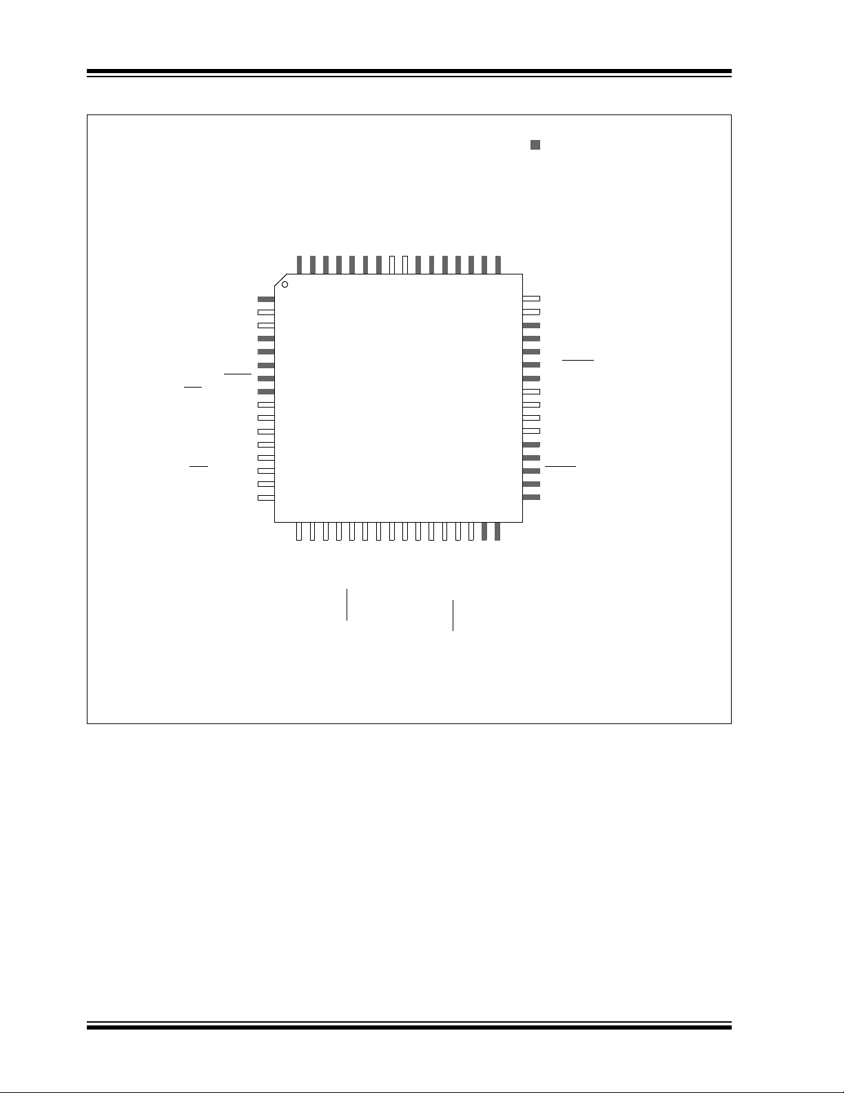
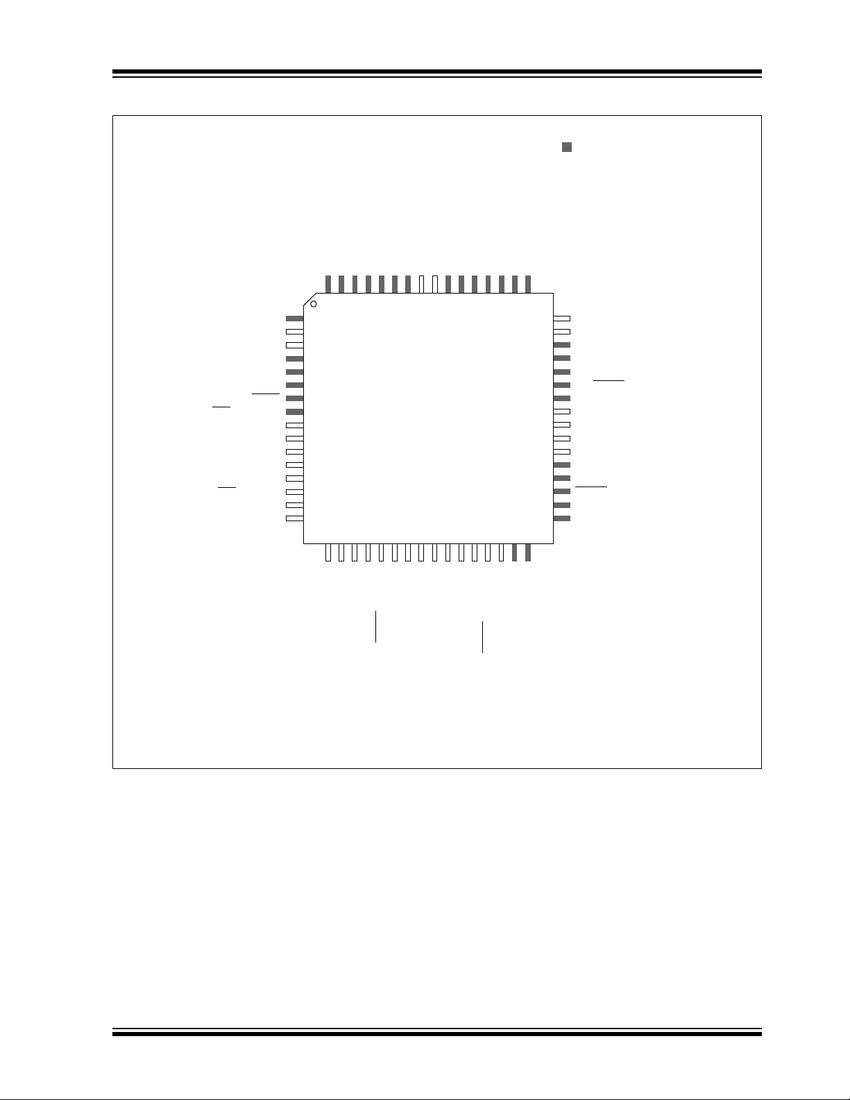
dsPIC33FJXXXGPX06/X08/X10
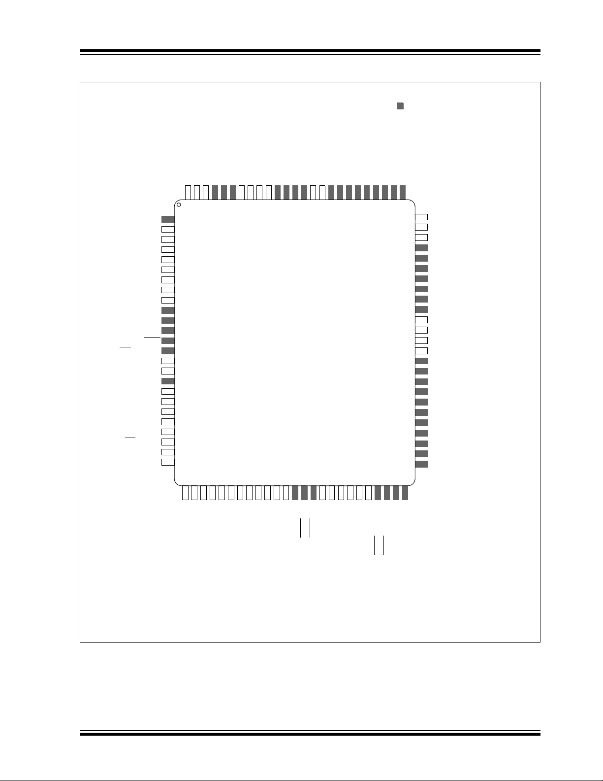
64-Pin TQFP
1
2
3
4
5
6
7
8
9
10
11
12
13
36
35
34
33
32
31
30
29
28
27
26
646362616059585756
14
15
16
171819202122232425
PGEC2/SOSCO/T1CK/CN0/RC14
PGED2/SOSCI/T4CK/CN1/RC13
OC1/RD0
IC4/INT4/RD11
IC2/U1CTS
/INT2/RD9
IC1/INT1/RD8
V
SS
OSC2/CLKO/RC15
OSC1/CLKIN/RC12
V
DD
SCL1/RG2
U1RTS
/SCK1/INT0/RF6
U1RX/SDI1/RF2
U1TX/SDO1/RF3
COFS/RG15
AN16/T2CK/T7CK/RC1
AN17/T3CK/T6CK/RC2
SCK2/CN8/RG6
SDI2/CN9/RG7
SDO2/CN10/RG8
MCLR
VSS
VDD
AN3/CN5/RB3
AN2/SS1
/CN4/RB2
PGEC3/AN1/V
REF-/CN3/RB1
PGED3/AN0/V
REF+/CN2/RB0
OC8/CN16/RD7
CSDO/RG13
CSDI/RG12
CSCK/RG14
V
CAP/VDDCORE
RG1
RF1
RG0
OC2/RD1
OC3/RD2
PGEC1/AN6/OCFA/RB6
PGED1/AN7/RB7
AVDD
AVSS
U2CTS/AN8/RB8
AN9/RB9
TMS/AN10/RB10
TDO/AN11/RB11
V
SS
VDD
TCK/AN12/RB12
TDI/AN13/RB13
U2RTS
/AN14/RB14
AN15/OCFB/CN12/RB15
U2TX/CN18/RF5
U2RX/CN17/RF4
SDA1/RG3
43
42
41
40
39
38
37
44
48
47
46
504951
545352
55
45
SS2
/CN11/RG9
AN5/IC8/CN7/RB5
AN4/IC7/CN6/RB4
IC3/INT3/RD10
VDD
RF0
OC4/RD3
OC7/CN15/RD6
OC6/IC6/CN14/RD5
OC5/IC5/CN13/RD4
dsPIC33FJ64GP206
dsPIC33FJ128GP206
= Pins are up to 5V tolerant
Pin Diagrams
DS70286C-page 4 © 2009 Microchip Technology Inc.
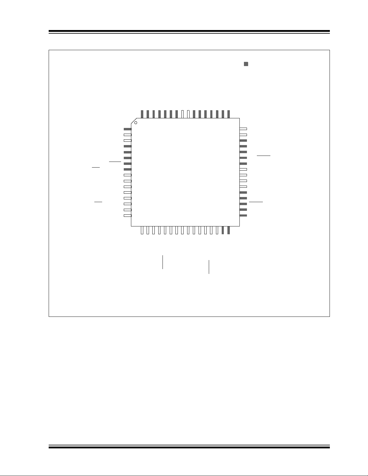
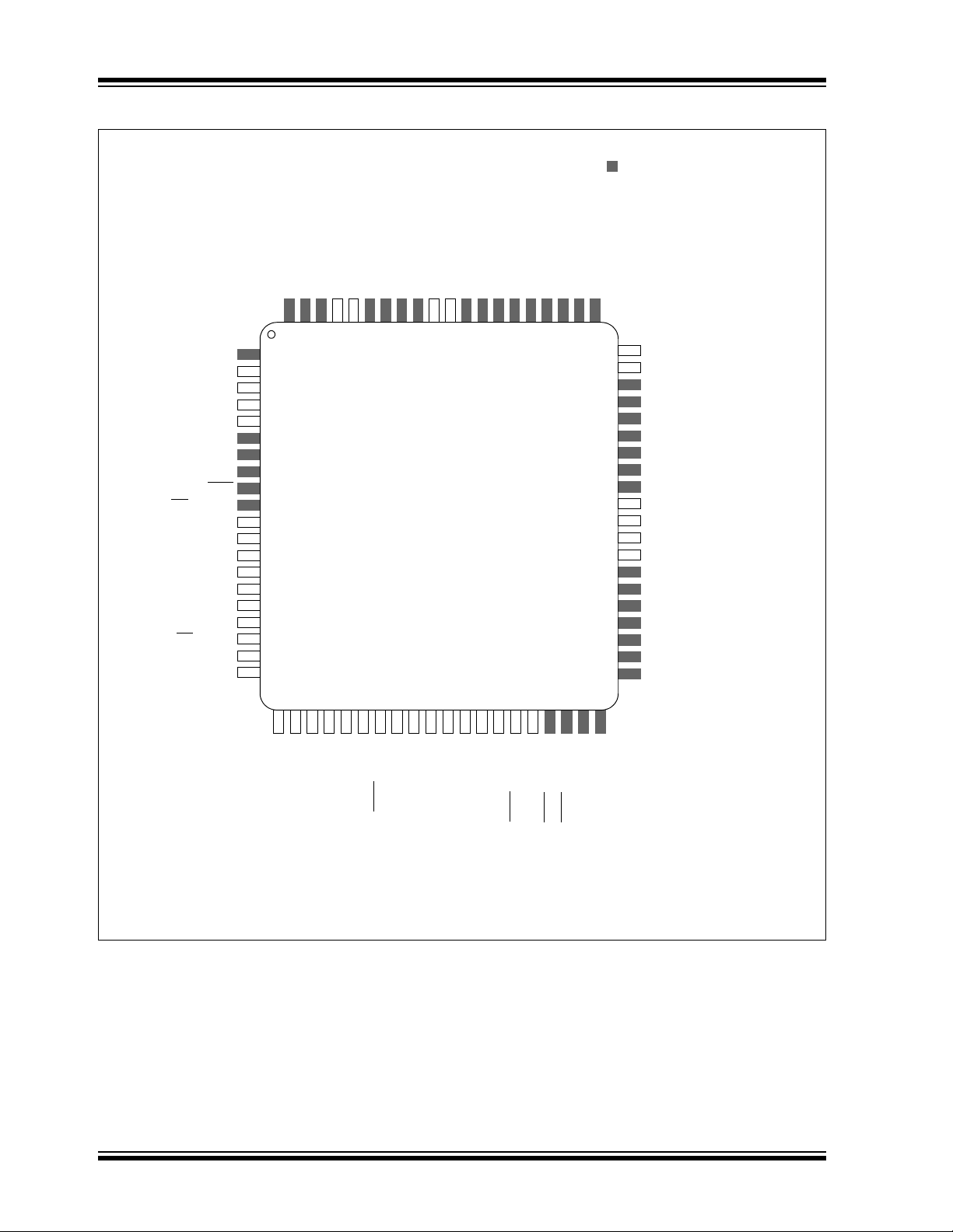
Pin Diagrams (Continued)
64-Pin TQFP
1
2
3
4
5
6
7
8
9
10
11
12
13
36
35
34
33
32
31
30
29
28
27
26
646362616059585756
14
15
16
171819202122232425
PGEC2/SOSCO/T1CK/CN0/RC14
PGED2/SOSCI/T4CK/CN1/RC13
OC1/RD0
IC4/INT4/RD11
IC2/U1CTS
/INT2/RD9
IC1/INT1/RD8
V
SS
OSC2/CLKO/RC15
OSC1/CLKIN/RC12
V
DD
SCL1/RG2
U1RTS
/SCK1/INT0/RF6
U1RX/SDI1/RF2
U1TX/SDO1/RF3
COFS/RG15
AN16/T2CK/T7CK/RC1
AN17/T3CK/T6CK/RC2
SCK2/CN8/RG6
SDI2/CN9/RG7
SDO2/CN10/RG8
MCLR
VSS
VDD
AN3/CN5/RB3
AN2/SS1
/CN4/RB2
PGEC3/AN1/V
REF-/CN3/RB1
PGED3/AN0/V
REF+/CN2/RB0
OC8/CN16/RD7
CSDO/RG13
CSDI/RG12
CSCK/RG14
V
CAP/VDDCORE
RG1
RF1
RG0
OC2/RD1
OC3/RD2
PGEC1/AN6/OCFA/RB6
PGED1/AN7/RB7
AVDD
AVSS
U2CTS/AN8/RB8
AN9/RB9
TMS/AN10/RB10
TDO/AN11/RB11
V
SS
VDD
TCK/AN12/RB12
TDI/AN13/RB13
U2RTS
/AN14/RB14
AN15/OCFB/CN12/RB15
U2TX/SCL2/CN18/RF5
U2RX/SDA2/CN17/RF4
SDA1/RG3
43
42
41
40
39
38
37
44
48
47
46
504951
545352
55
45
SS2
/CN11/RG9
AN5/IC8/CN7/RB5
AN4/IC7/CN6/RB4
IC3/INT3/RD10
VDD
RF0
OC4/RD3
OC7/CN15/RD6
OC6/IC6/CN14/RD5
OC5/IC5/CN13/RD4
dsPIC33FJ64GP306
dsPIC33FJ128GP306
= Pins are up to 5V tolerant
dsPIC33FJXXXGPX06/X08/X10
© 2009 Microchip Technology Inc. DS70286C-page 5

dsPIC33FJXXXGPX06/X08/X10
64-Pin TQFP
1
2
3
4
5
6
7
8
9
10
11
12
13
36
35
34
33
32
31
30
29
28
27
26
646362616059585756
14
15
16
171819202122232425
PGEC2/SOSCO/T1CK/CN0/RC14
PGED2/SOSCI/T4CK/CN1/RC13
OC1/RD0
IC4/INT4/RD11
IC2/U1CTS
/INT2/RD9
IC1/INT1/RD8
V
SS
OSC2/CLKO/RC15
OSC1/CLKIN/RC12
V
DD
SCL1/RG2
U1RTS
/SCK1/INT0/RF6
U1RX/SDI1/RF2
U1TX/SDO1/RF3
COFS/RG15
AN16/T2CK/T7CK/RC1
AN17/T3CK/T6CK/RC2
SCK2/CN8/RG6
SDI2/CN9/RG7
SDO2/CN10/RG8
MCLR
VSS
VDD
AN3/CN5/RB3
AN2/SS1
/CN4/RB2
PGEC3/AN1/V
REF-/CN3/RB1
PGED3/AN0/V
REF+/CN2/RB0
OC8/CN16/RD7
CSDO/RG13
CSDI/RG12
CSCK/RG14
V
CAP/VDDCORE
RG1
C1TX/RF1
RG0
OC2/RD1
OC3/RD2
PGEC1/AN6/OCFA/RB6
PGED1/AN7/RB7
AVDD
AVSS
U2CTS/AN8/RB8
AN9/RB9
TMS/AN10/RB10
TDO/AN11/RB11
V
SS
VDD
TCK/AN12/RB12
TDI/AN13/RB13
U2RTS
/AN14/RB14
AN15/OCFB/CN12/RB15
U2TX/SCL2/CN18/RF5
U2RX/SDA2/CN17/RF4
SDA1/RG3
43
42
41
40
39
38
37
44
48
47
46
504951
545352
55
45
SS2
/CN11/RG9
AN5/IC8/CN7/RB5
AN4/IC7/CN6/RB4
IC3/INT3/RD10
VDD
C1RX/RF0
OC4/RD3
OC7/CN15/RD6
OC6/IC6/CN14/RD5
OC5/IC5/CN13/RD4
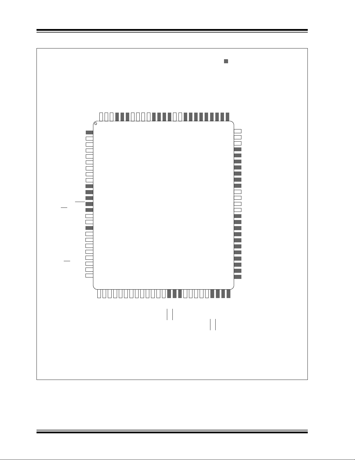
dsPIC33FJ256GP506
= Pins are up to 5V tolerant
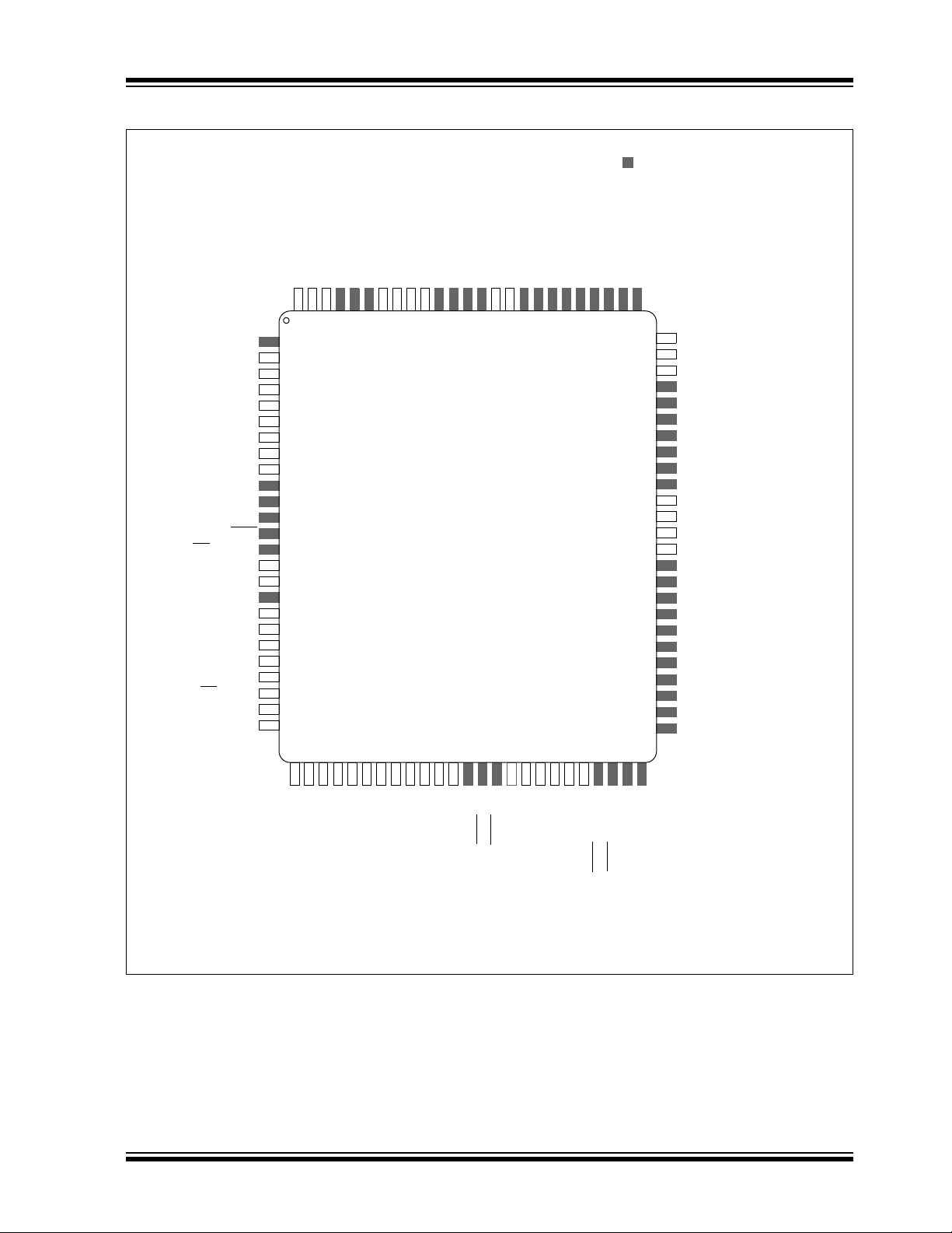
Pin Diagrams (Continued)
DS70286C-page 6 © 2009 Microchip Technology Inc.
Pin Diagrams (Continued)
64-Pin TQFP
1
2
3
4
5
6
7
8
9
10
11
12
13
36
35
34
33
32
31
30
29
28
27
26
646362616059585756
14
15
16
171819202122232425
PGEC2/SOSCO/T1CK/CN0/RC14
PGED2/SOSCI/T4CK/CN1/RC13
OC1/RD0
IC4/INT4/RD11
IC2/U1CTS
/INT2/RD9
IC1/INT1/RD8
V
SS
OSC2/CLKO/RC15
OSC1/CLKIN/RC12
V
DD
SCL1/RG2
U1RTS
/SCK1/INT0/RF6
U1RX/SDI1/RF2
U1TX/SDO1/RF3
COFS/RG15
AN16/T2CK/T7CK/RC1
AN17/T3CK/T6CK/RC2
SCK2/CN8/RG6
SDI2/CN9/RG7
SDO2/CN10/RG8
MCLR
VSS
VDD
AN3/CN5/RB3
AN2/SS1
/CN4/RB2
PGEC3/AN1/V
REF-/CN3/RB1
PGED3/AN0/V
REF+/CN2/RB0
OC8/CN16/RD7
CSDO/RG13
CSDI/RG12
CSCK/RG14
V
CAP/VDDCORE
C2TX/RG1
C1TX/RF1
C2RX/RG0
OC2/RD1
OC3/RD2
PGEC1/AN6/OCFA/RB6
PGED1/AN7/RB7
AVDD
AVSS
U2CTS/AN8/RB8
AN9/RB9
TMS/AN10/RB10
TDO/AN11/RB11
V
SS
VDD
TCK/AN12/RB12
TDI/AN13/RB13
U2RTS
/AN14/RB14
AN15/OCFB/CN12/RB15
U2TX/SCL2/CN18/RF5
U2RX/SDA2/CN17/RF4
SDA1/RG3
43
42
41
40
39
38
37
44
48
47
46
504951
545352
55
45
SS2
/CN11/RG9
AN5/IC8/CN7/RB5
AN4/IC7/CN6/RB4
IC3/INT3/RD10
VDD
C1RX/RF0
OC4/RD3
OC7/CN15/RD6
OC6/IC6/CN14/RD5
OC5/IC5/CN13/RD4
dsPIC33FJ64GP706
dsPIC33FJ128GP706
= Pins are up to 5V tolerant
dsPIC33FJXXXGPX06/X08/X10
© 2009 Microchip Technology Inc. DS70286C-page 7
dsPIC33FJXXXGPX06/X08/X10
80-Pin TQFP
727473
7170696867666564636261
20
2
3
4
5
6
7
8
9
10
11
12
13
14
15
16
50
49
48
47
46
45
44
21
41
40
39
38
37
36
35
34
2324252627282930313233
dsPIC33FJ64GP708
17
18
19
75
1
57
56
55
54
53
52
51
60
59
58
43
42
767877
792280
IC5/RD12
OC4/RD3
OC3/RD2
OC2/RD1
CSCK/RG14
AN23/CN23/RA7
AN22/CN22/RA6
C2RX/RG0
C2TX/RG1
C1TX/RF1
C1RX/RF0
CSDO/RG13
CSDI/RG12
OC8/CN16/RD7
OC6/CN14/RD5
OC1/RD0
IC4/RD11
IC2/RD9
IC1/RD8
IC3/RD10
V
SS
OSC1/CLKIN/RC12
V
DD
SCL1/RG2
U1RX/RF2
U1TX/RF3
PGEC2/SOSCO/T1CK/CN0/RC14
PGED2/SOSCI/CN1/RC13
V
REF
+/RA10
V
REF
-/RA9
AV
DD
AV
SS
U2CTS/AN8/RB8
AN9/RB9
AN10/RB10
AN11/RB11
V
DD
U2RX/CN17/RF4
IC8/U1RTS
/CN21/RD15
U2TX/CN18/RF5
PGEC1/AN6/OCFA/RB6
PGED1/AN7/RB7
AN17/T3CK/T6CK/RC2
AN18/T4CK/T9CK/RC3
AN19/T5CK/T8CK/RC4
SCK2/CN8/RG6
SDI2/CN9/RG7
SDO2/CN10/RG8
MCLR
SS2/CN11/RG9
AN4/CN6/RB4
AN3/CN5/RB3
AN2/SS1
/CN4/RB2
PGEC3/AN1/CN3/RB1
PGED3/AN0/CN2/RB0
V
SS
V
DD
COFS/RG15
AN16/T2CK/T7CK/RC1
TDO/AN21/INT2/RA13
TMS/AN20/INT1/RA12
TCK/AN12/RB12
TDI/AN13/RB13
U2RTS
/AN14/RB14
AN15/OCFB/CN12/RB15
V
DDVCAP
/V
DDCORE
OC5/CN13/RD4
IC6/CN19/RD13
SDA1/RG3
SDI1/RF7
SDO1/RF8
AN5/CN7/RB5
V
SS
OSC2/CLKO/RC15
OC7/CN15/RD6
SCK1/INT0/RF6
IC7/U1CTS/CN20/RD14
SDA2/INT4/RA3
SCL2/INT3/RA2
dsPIC33FJ128GP708
= Pins are up to 5V tolerant
Pin Diagrams (Continued)
DS70286C-page 8 © 2009 Microchip Technology Inc.
Pin Diagrams (Continued)
9294939190898887868584838281807978
20
2
3
4
5
6
7
8
9
10
11
12
13
14
15
16
65
64
63
62
61
60
59
26
56
45
44
43
42
41
40
39
2829303132333435363738
17
18
19
21
22
95
1
76
77
72
71
70
69
68
67
66
75
74
73
58
57
24
23
25
969897
99
27
4647484950
55
54
53
52
51
OC6/CN14/RD5
OC5/CN13/RD4
IC6/CN19/RD13
IC5/RD12
OC4/RD3
OC3/RD2
OC2/RD1
AN23/CN23/RA7
AN22/CN22/RA6
AN26/RE2
CSDO/RG13
CSDI/RG12
CSCK/RG14
AN25/RE1
AN24/RE0
RG0
AN28/RE4
AN27/RE3
RF0
V
CAP
/V
DDCORE
PGED2/SOSCI/CN1/RC13
OC1/RD0
IC3/RD10
IC2/RD9
IC1/RD8
IC4/RD11
SDA2/RA3
SCL2/RA2
OSC2/CLKO/RC15
OSC1/CLKIN/RC12
V
DD
SCL1/RG2
SCK1/INT0/RF6
SDI1/RF7
SDO1/RF8
SDA1/RG3
U1RX/RF2
U1TX/RF3
V
SS
PGEC2/SOSCO/T1CK/CN0/RC14
V
REF
+/RA10
V
REF
-/RA9
AV
DD
AV
SS
AN8/RB8
AN9/RB9
AN10/RB10
AN11/RB11
V
DD
U2CTS/RF12
U2RTS
/RF13
IC7/U1CTS
/CN20/RD14
IC8/U1RTS
/CN21/RD15
V
DD
V
SS
PGEC1/AN6/OCFA/RB6
PGED1/AN7/RB7
U2TX/CN18/RF5
U2RX/CN17/RF4
AN29/RE5
AN30/RE6
AN31/RE7
AN16/T2CK/T7CK/RC1
AN17/T3CK/T6CK/RC2
AN18/T4CK/T9CK/RC3
AN19/T5CK/T8CK/RC4
SCK2/CN8/RG6
V
DD
TMS/RA0
AN20/INT1/RA12
AN21/INT2/RA13
AN5/CN7/RB5
AN4/CN6/RB4
AN3/CN5/RB3
AN2/SS1
/CN4/RB2
SDI2/CN9/RG7
SDO2/CN10/RG8
PGEC3/AN1/CN3/RB1
PGED3/AN0/CN2/RB0
COFS/RG15
V
DD
SS2/CN11/RG9
MCLR
AN12/RB12
AN13/RB13
AN14/RB14
AN15/OCFB/CN12/RB15
RG1
RF1
OC8/CN16/RD7
OC7/CN15/RD6
TDO/RA5
INT4/RA15
INT3/RA14
V
SS
V
SS
V
SS
V
DD
TDI/RA4
TCK/RA1
100-Pin TQFP
dsPIC33FJ64GP310
dsPIC33FJ128GP310
100
= Pins are up to 5V tolerant
dsPIC33FJXXXGPX06/X08/X10
© 2009 Microchip Technology Inc. DS70286C-page 9
dsPIC33FJXXXGPX06/X08/X10
9294939190898887868584838281807978
20
2
3
4
5
6
7
8
9
10
11
12
13
14
15
16
65
64
63
62
61
60
59
26
56
45
44
43
42
41
40
39
2829303132333435363738
17
18
19
21
22
95
1
76
77
72
71
70
69
68
67
66
75
74
73
58
57
24
23
25
969897
99
27
4647484950
55
54
53
52
51
OC6/CN14/RD5
OC5/CN13/RD4
IC6/CN19/RD13
IC5/RD12
OC4/RD3
OC3/RD2
OC2/RD1
AN23/CN23/RA7
AN22/CN22/RA6
AN26/RE2
CSDO/RG13
CSDI/RG12
CSCK/RG14
AN25/RE1
AN24/RE0
RG0
AN28/RE4
AN27/RE3
C1RX/RF0
V
CAP
/V
DDCORE
PGED2/SOSCI/CN1/RC13
OC1/RD0
IC3/RD10
IC2/RD9
IC1/RD8
IC4/RD11
SDA2/RA3
SCL2/RA2
OSC2/CLKO/RC15
OSC1/CLKIN/RC12
V
DD
SCL1/RG2
SCK1/INT0/RF6
SDI1/RF7
SDO1/RF8
SDA1/RG3
U1RX/RF2
U1TX/RF3
V
SS
PGEC2/SOSCO/T1CK/CN0/RC14
V
REF
+/RA10
V
REF
-/RA9
AV
DD
AV
SS
AN8/RB8
AN9/RB9
AN10/RB10
AN11/RB11
V
DD
U2CTS/RF12
U2RTS
/RF13
IC7/U1CTS
/CN20/RD14
IC8/U1RTS
/CN21/RD15
V
DD
V
SS
PGEC1/AN6/OCFA/RB6
PGED1/AN7/RB7
U2TX/CN18/RF5
U2RX/CN17/RF4
AN29/RE5
AN30/RE6
AN31/RE7
AN16/T2CK/T7CK/RC1
AN17/T3CK/T6CK/RC2
AN18/T4CK/T9CK/RC3
AN19/T5CK/T8CK/RC4
SCK2/CN8/RG6
V
DD
TMS/RA0
AN20/INT1/RA12
AN21/INT2/RA13
AN5/CN7/RB5
AN4/CN6/RB4
AN3/CN5/RB3
AN2/SS1
/CN4/RB2
SDI2/CN9/RG7
SDO2/CN10/RG8
PGEC3/AN1/CN3/RB1
PGED3/AN0/CN2/RB0
COFS/RG15
V
DD
SS2/CN11/RG9
MCLR
AN12/RB12
AN13/RB13
AN14/RB14
AN15/OCFB/CN12/RB15
RG1
C1TX/RF1
OC8/CN16/RD7
OC7/CN15/RD6
TDO/RA5
INT4/RA15
INT3/RA14
V
SS
V
SS
V
SS
V
DD
TDI/RA4
TCK/RA1
100-Pin TQFP
dsPIC33FJ256GP510
100
= Pins are up to 5V tolerant
Pin Diagrams (Continued)
DS70286C-page 10 © 2009 Microchip Technology Inc.
Pin Diagrams (Continued)
9294939190898887868584838281807978
20
2
3
4
5
6
7
8
9
10
11
12
13
14
15
16
65
64
63
62
61
60
59
26
56
45
44
43
42
41
40
39
2829303132333435363738
17
18
19
21
22
95
1
76
77
72
71
70
69
68
67
66
75
74
73
58
57
24
23
25
969897
99
27
4647484950
55
54
53
52
51
OC6/CN14/RD5
OC5/CN13/RD4
IC6/CN19/RD13
IC5/RD12
OC4/RD3
OC3/RD2
OC2/RD1
AN23/CN23/RA7
AN22/CN22/RA6
AN26/RE2
CSDO/RG13
CSDI/RG12
CSCK/RG14
AN25/RE1
AN24/RE0
C2RX/RG0
AN28/RE4
AN27/RE3
C1RX/RF0
V
CAP
/V
DDCORE
PGED2/SOSCI/CN1/RC13
OC1/RD0
IC3/RD10
IC2/RD9
IC1/RD8
IC4/RD11
SDA2/RA3
SCL2/RA2
OSC2/CLKO/RC15
OSC1/CLKIN/RC12
V
DD
SCL1/RG2
SCK1/INT0/RF6
SDI1/RF7
SDO1/RF8
SDA1/RG3
U1RX/RF2
U1TX/RF3
V
SS
PGEC2/SOSCO/T1CK/CN0/RC14
V
REF
+/RA10
V
REF
-/RA9
AV
DD
AV
SS
AN8/RB8
AN9/RB9
AN10/RB10
AN11/RB11
V
DD
U2CTS/RF12
U2RTS
/RF13
IC7/U1CTS
/CN20/RD14
IC8/U1RTS
/CN21/RD15
V
DD
V
SS
PGEC1/AN6/OCFA/RB6
PGED1/AN7/RB7
U2TX/CN18/RF5
U2RX/CN17/RF4
AN29/RE5
AN30/RE6
AN31/RE7
AN16/T2CK/T7CK/RC1
AN17/T3CK/T6CK/RC2
AN18/T4CK/T9CK/RC3
AN19/T5CK/T8CK/RC4
SCK2/CN8/RG6
V
DD
TMS/RA0
AN20/INT1/RA12
AN21/INT2/RA13
AN5/CN7/RB5
AN4/CN6/RB4
AN3/CN5/RB3
AN2/SS1
/CN4/RB2
SDI2/CN9/RG7
SDO2/CN10/RG8
PGEC3/AN1/CN3/RB1
PGED3/AN0/CN2/RB0
COFS/RG15
V
DD
SS2/CN11/RG9
MCLR
AN12/RB12
AN13/RB13
AN14/RB14
AN15/OCFB/CN12/RB15
C2TX/RG1
C1TX/RF1
OC8/CN16/RD7
OC7/CN15/RD6
TDO/RA5
INT4/RA15
INT3/RA14
V
SS
V
SS
V
SS
V
DD
TDI/RA4
TCK/RA1
100-Pin TQFP
dsPIC33FJ128GP710
100
dsPIC33FJ256GP710
dsPIC33FJ64GP710
= Pins are up to 5V tolerant
dsPIC33FJXXXGPX06/X08/X10
© 2009 Microchip Technology Inc. DS70286C-page 11

dsPIC33FJXXXGPX06/X08/X10
Table of Contents
dsPIC33F Product Families ................................................................................................................................................................... 3
1.0 Device Overview ........................................................................................................................................................................ 13
2.0 Guidelines for Getting Started with 16-Bit Digital Signal Controllers .......................................................................................... 17
3.0 CPU............................................................................................................................................................................................ 21
4.0 Memory Organization ................................................................................................................................................................. 33
5.0 Flash Program Memory.............................................................................................................................................................. 71
6.0 Reset ......................................................................................................................................................................................... 77
7.0 Interrupt Controller ..................................................................................................................................................................... 81
8.0 Direct Memory Access (DMA) .................................................................................................................................................. 127
9.0 Oscillator Configuration ............................................................................................................................................................ 137
10.0 Power-Saving Features ............................................................................................................................................................ 147
11.0 I/O Ports ................................................................................................................................................................................... 155
12.0 Timer1 ...................................................................................................................................................................................... 157
13.0 Timer2/3, Timer4/5, Timer6/7 and Timer8/9 ............................................................................................................................ 159
14.0 Input Capture............................................................................................................................................................................ 165
15.0 Output Compare ....................................................................................................................................................................... 167
16.0 Serial Peripheral Interface (SPI)............................................................................................................................................... 171
17.0 Inter-Integrated Circuit™ (I
18.0 Universal Asynchronous Receiver Transmitter (UART) ........................................................................................................... 185
19.0 Enhanced CAN (ECAN™) Module ........................................................................................................................................... 191
20.0 Data Converter Interface (DCI) Module.................................................................................................................................... 217
21.0 10-Bit/12-Bit Analog-to-Digital Converter (ADC) ...................................................................................................................... 225
22.0 Special Features ...................................................................................................................................................................... 237
23.0 Instruction Set Summary .......................................................................................................................................................... 245
24.0 Development Support............................................................................................................................................................... 253
25.0 Electrical Characteristics .......................................................................................................................................................... 257
26.0 Packaging Information.............................................................................................................................................................. 297
Appendix A: Revision History............................................................................................................................................................. 307
Index ................................................................................................................................................................................................. 313
The Microchip Web Site ..................................................................................................................................................................... 317
Customer Change Notification Service .............................................................................................................................................. 317
Customer Support .............................................................................................................................................................................. 317
Reader Response .............................................................................................................................................................................. 318
Product Identification System............................................................................................................................................................. 319
2
C™).............................................................................................................................................. 177
TO OUR VALUED CUSTOMERS
It is our intention to provide our valued customers with the best documentation possible to ensure successful use of your Microchip
products. To this end, we will continue to improve our publications to better suit your needs. Our publications will be refined and
enhanced as new volumes and updates are introduced.
If you have any questions or comments regarding this publication, please contact the Marketing Communications Department via
E-mail at docerrors@microchip.com or fax the Reader Response Form in the back of this data sheet to (480) 792-4150. We
welcome your feedback.
Most Current Data Sheet
To obtain the most up-to-date version of this data sheet, please register at our Worldwide Web site at:
http://www.microchip.com
You can determine the version of a data sheet by examining its literature number found on the bottom outside corner of any page.
The last character of the literature number is the version number, (e.g., DS30000A is version A of document DS30000).
Errata
An errata sheet, describing minor operational differences from the data sheet and recommended workarounds, may exist for current
devices. As device/documentation issues become known to us, we will publish an errata sheet. The errata will specify the revision
of silicon and revision of document to which it applies.
To determine if an errata sheet exists for a particular device, please check with one of the following:
• Microchip’s Worldwide Web site; http://www.microchip.com
• Your local Microchip sales office (see last page)
When contacting a sales office, please specify which device, revision of silicon and data sheet (include literature number) you are
using.
Customer Notification System
Register on our web site at www.microchip.com to receive the most current information on all of our products.
DS70286C-page 12 © 2009 Microchip Technology Inc.

dsPIC33FJXXXGPX06/X08/X10
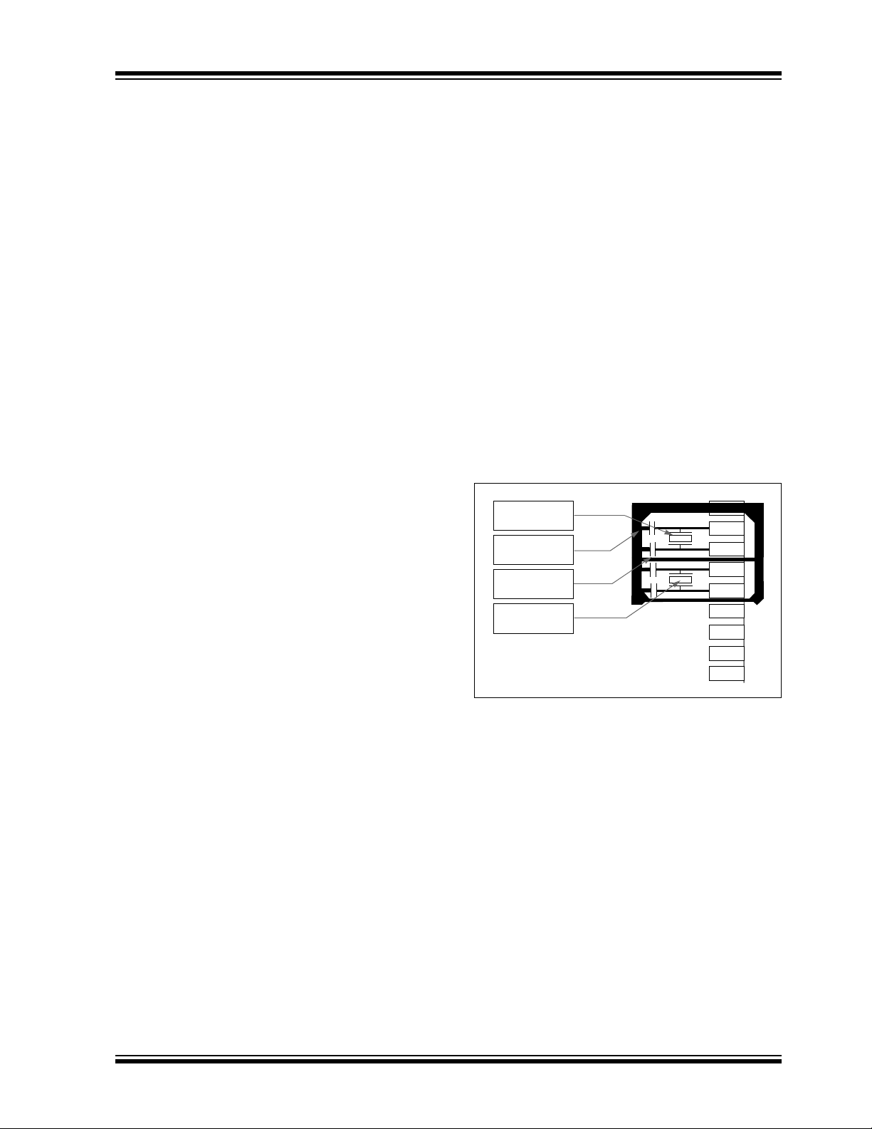
1.0 DEVICE OVERVIEW
Note: This data sheet summarizes the features
of the dsPIC33FJXXXGPX06/X08/X10
family of devices. However, it is not
intended to be a comprehensive reference
source. To complement the information in
this data sheet, refer to the latest family
reference sections of the “dsPIC33F
Family Reference Manual”, which is
available from the Microchip web site
(www.microchip.com).
This document contains device specific information for
the following devices:
• dsPIC33FJ64GP206
• dsPIC33FJ64GP306
• dsPIC33FJ64GP310
• dsPIC33FJ64GP706
• dsPIC33FJ64GP708
• dsPIC33FJ64GP710
• dsPIC33FJ128GP206
• dsPIC33FJ128GP306
• dsPIC33FJ128GP310
• dsPIC33FJ128GP706
• dsPIC33FJ128GP708
• dsPIC33FJ128GP710
• dsPIC33FJ256GP506
• dsPIC33FJ256GP510
• dsPIC33FJ256GP710
The dsPIC33FJXXXGPX06/X08/X10 General Purpose
Family of device includes devices with a wide range of
pin counts (64, 80 and 100), different program memory
sizes (64 Kbytes, 128 Kbytes and 256 Kbytes) and
different RAM sizes (8 Kbytes, 16 Kbytes and
30 Kbytes).
This feature makes the family suitable for a wide variety
of high-performance digital signal control applications.
The device is pin compatible with the PIC24H family of
devices, and also share a very high degree of
compatibility with the dsPIC30F family devices. This
allows for easy migration between device families as may
be necessitated by the specific functionality,
computational resource and system cost requirements of
the application.
The dsPIC33FJXXXGPX06/X08/X10 device family
employs a powerful 16-bit architecture that seamlessly
integrates the control features of a Microcontroller
(MCU) with the computational capabilities of a Digital
Signal Processor (DSP). The resulting functionality is
ideal for applications that rely on high-speed, repetitive
computations, as well as control.
The DSP engine, dual 40-bit accumulators, hardware
support for division operations, barrel shifter, 17 x 17
multiplier, a large array of 16-bit working registers and
a wide variety of data addressing modes, together
provide the dsPIC33FJXXXGPX06/X08/X10 Central
Processing Unit (CPU) with extensive mathematical
processing capability. Flexible and deterministic
interrupt handling, coupled with a powerful array of
peripherals, renders the
dsPIC33FJXXXGPX06/X08/X10 devices suitable for
control applications. Further, Direct Memory Access
(DMA) enables overhead-free transfer of data between
several peripherals and a dedicated DMA RAM.
Reliable, field programmable Flash program memory
ensures scalability of applications that use
dsPIC33FJXXXGPX06/X08/X10 devices.
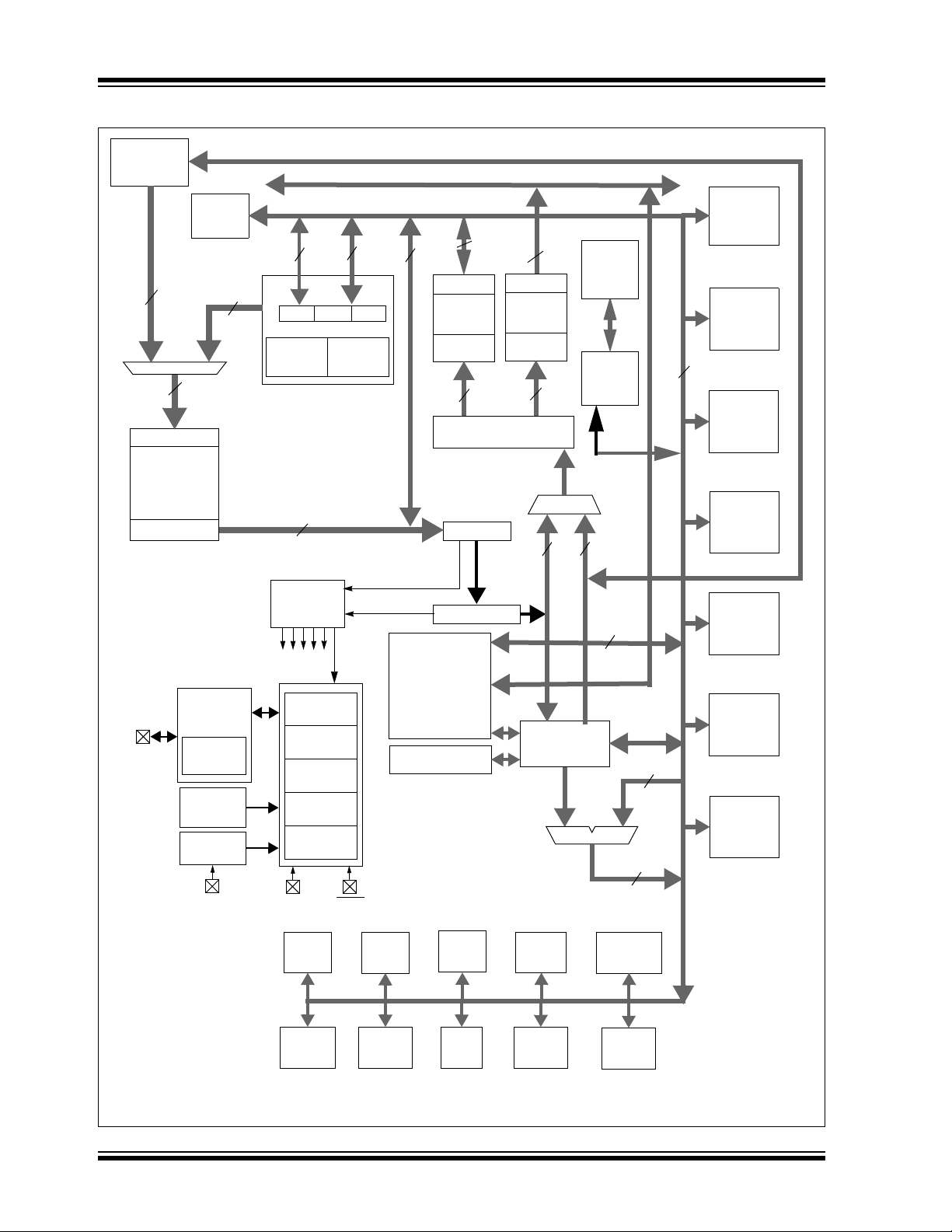
Figure 1-1 illustrates a general block diagram of the
various core and peripheral modules in the
dsPIC33FJXXXGPX06/X08/X10 family of devices.
Table 1-1 provides the functions of the various pins
illustrated in the pinout diagrams.
© 2009 Microchip Technology Inc. DS70286C-page 13
16
OSC1/CLKI
OSC2/CLKO
V
DD, VSS
Timing
Generation
MCLR
Power-up
Timer
Oscillator
Star t- up Timer
Power-on
Reset
Watchdog
Timer
Brown-out
Reset
Precision
Reference
Band Gap
FRC/LPRC
Oscillators
Regulator
Voltage
VCAP/VDDCORE
UART1,2
ECAN1,2
DCI
IC1-8
SPI1,2
I2C1,2
OC/
PORTA
Note: Not all pins or features are implemented on all device pinout configurations. See pinout diagrams for the specific pins
and features present on each device.
PWM1-8
CN1-23
Instruction
Decode and
Control
PCH PCL
16
Program Counter
16-bit ALU
23
23
24
23
Instruction Reg
PCU
16 x 16
W Register Array
ROM Latch
16
EA MUX
16
16
8
Interrupt
Controller
PSV and Table
Data Access
Control Block
Stac k
Control
Logic
Loop
Control
Logic
Data Latch
Address
Latch
Address Latch
Program Memory
Data Latch
Literal Data
16
16
16
16
Data Latch
Address
Latch
16
X RAM
Y RAM
16
Y Data Bus
X Data Bus
DSP Engine
Divide Support
16
DMA
RAM
DMA
Controller
Control Signals
to Various Blocks
ADC1,2
Timers
PORTB
PORTC
PORTD
PORTE
PORTF
PORTG
Address Generator Units
1-9
dsPIC33FJXXXGPX06/X08/X10
FIGURE 1-1: dsPIC33FJXXXGPX06/X08/X10 GENERAL BLOCK DIAGRAM
DS70286C-page 14 © 2009 Microchip Technology Inc.

dsPIC33FJXXXGPX06/X08/X10
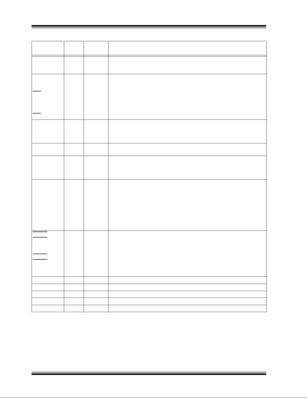
TABLE 1-1: PINOUT I/O DESCRIPTIONS
Pin Name
AN0-AN31 I Analog Analog input channels.
DD P P Positive supply for analog modules. This pin must be connected at all times.
AV
AV
SS P P Ground reference for analog modules.
CLKI
CLKO
CN0-CN23 I ST Input change notification inputs.
COFS
CSCK
CSDI
CSDO
C1RX
C1TX
C2RX
C2TX
PGED1
PGEC1
PGED2
PGEC2
PGED3
PGEC3
IC1-IC8 I ST Capture inputs 1 through 8.
INT0
INT1
INT2
INT3
INT4
MCLR
OCFA
OCFB
OC1-OC8
OSC1
OSC2
RA0-RA7
RA9-RA10
RA12-RA15
RB0-RB15 I/O ST PORTB is a bidirectional I/O port.
RC1-RC4
RC12-RC15
RD0-RD15 I/O ST PORTD is a bidirectional I/O port.
RE0-RE7 I/O ST PORTE is a bidirectional I/O port.
RF0-RF8
RF12-RF13
Legend: CMOS = CMOS compatible input or output; Analog = Analog input; P = Power
ST = Schmitt Trigger input with CMOS levels; O = Output; I = Input
Pin
Type
I
O
I/O
I/O
I
O
I
O
I
O
I/O
I
I/O
I
I/O
I
I
I
I
I
I
I/P ST Master Clear (Reset) input. This pin is an active-low Reset to the device.
I
I
O
I
I/O
I/O
I/O
I/O
I/O
I/O
I/O
I/O
Buffer
Typ e
ST/CMOS—External clock source input. Always associated with OSC1 pin function.
Oscillator crystal output. Connects to crystal or resonator in Crystal Oscillator
mode. Optionally functions as CLKO in RC and EC modes. Always associated
with OSC2 pin function.
Can be software programmed for internal weak pull-ups on all inputs.
ST
ST
ST
—
ST
—
ST
—
ST
ST
ST
ST
ST
ST
ST
ST
ST
ST
ST
ST
ST
—
ST/CMOS—Oscillator crystal input. ST buffer when configured in RC mode;
ST
ST
ST
ST
ST
ST
ST
Data Converter Interface frame synchronization pin.
Data Converter Interface serial clock input/output pin.
Data Converter Interface serial data input pin.
Data Converter Interface serial data output pin.
ECAN1 bus receive pin.
ECAN1 bus transmit pin.
ECAN2 bus receive pin.
ECAN2 bus transmit pin.
Data I/O pin for programming/debugging communication channel 1.
Clock input pin for programming/debugging communication channel 1.
Data I/O pin for programming/debugging communication channel 2.
Clock input pin for programming/debugging communication channel 2.
Data I/O pin for programming/debugging communication channel 3.
Clock input pin for programming/debugging communication channel 3.
External interrupt 0.
External interrupt 1.
External interrupt 2.
External interrupt 3.
External interrupt 4.
Compare Fault A input (for Compare Channels 1, 2, 3 and 4).
Compare Fault B input (for Compare Channels 5, 6, 7 and 8).
Compare outputs 1 through 8.
CMOS otherwise.
Oscillator crystal output. Connects to crystal or resonator in Crystal Oscillator
mode. Optionally functions as CLKO in RC and EC modes.
PORTA is a bidirectional I/O port.
PORTC is a bidirectional I/O port.
PORTF is a bidirectional I/O port.
Description
© 2009 Microchip Technology Inc. DS70286C-page 15
dsPIC33FJXXXGPX06/X08/X10
TABLE 1-1: PINOUT I/O DESCRIPTIONS (CONTINUED)
Pin Name
RG0-RG3
RG6-RG9
RG12-RG15
SCK1
SDI1
SDO1
SS1
SCK2
SDI2
SDO2
SS2
SCL1
SDA1
SCL2
SDA2
SOSCI
SOSCO
TMS
TCK
TDI
TDO
T1CK
T2CK
T3CK
T4CK
T5CK
T6CK
T7CK
T8CK
T9CK
U1CTS
U1RTS
U1RX
U1TX
U2CTS
U2RTS
U2RX
U2TX
DD P — Positive supply for peripheral logic and I/O pins.
V
V
CAP/VDDCORE P — CPU logic filter capacitor connection.
VSS P — Ground reference for logic and I/O pins.
V
REF+ I Analog Analog voltage reference (high) input.
V
REF- I Analog Analog voltage reference (low) input.
Legend: CMOS = CMOS compatible input or output; Analog = Analog input; P = Power
ST = Schmitt Trigger input with CMOS levels; O = Output; I = Input
Pin
Type
I/O
I/O
I/O
I/O
I
O
I/O
I/O
I
O
I/O
I/O
I/O
I/O
I/O
I
O
I
I
I
O
I
I
I
I
I
I
I
I
I
I
O
I
O
I
O
I
O
Buffer
Typ e
ST
ST
ST
ST
ST
—
ST
ST
ST
—
ST
ST
ST
ST
ST
ST/CMOS—32.768 kHz low-power oscillator crystal input; CMOS otherwise.
ST
ST
ST
—
ST
ST
ST
ST
ST
ST
ST
ST
ST
ST
—
ST
—
ST
—
ST
—
PORTG is a bidirectional I/O port.
Synchronous serial clock input/output for SPI1.
SPI1 data in.
SPI1 data out.
SPI1 slave synchronization or frame pulse I/O.
Synchronous serial clock input/output for SPI2.
SPI2 data in.
SPI2 data out.
SPI2 slave synchronization or frame pulse I/O.
Synchronous serial clock input/output for I2C1.
Synchronous serial data input/output for I2C1.
Synchronous serial clock input/output for I2C2.
Synchronous serial data input/output for I2C2.
32.768 kHz low-power oscillator crystal output.
JTAG Test mode select pin.
JTAG test clock input pin.
JTAG test data input pin.
JTAG test data output pin.
Timer1 external clock input.
Timer2 external clock input.
Timer3 external clock input.
Timer4 external clock input.
Timer5 external clock input.
Timer6 external clock input.
Timer7 external clock input.
Timer8 external clock input.
Timer9 external clock input.
UART1 clear to send.
UART1 ready to send.
UART1 receive.
UART1 transmit.
UART2 clear to send.
UART2 ready to send.
UART2 receive.
UART2 transmit.
Description
DS70286C-page 16 © 2009 Microchip Technology Inc.

dsPIC33FJXXXGPX06/X08/X10
2.0 GUIDELINES FOR GETTING STARTED WITH 16-BIT DIGITAL SIGNAL CONTROLLERS
Note: This data sheet summarizes the features
of the dsPIC33FJXXXGPX06/X08/X10
family of devices. It is not intended to be a
comprehensive reference source. To
complement the information in this data
sheet, refer to the “dsPIC33F Family
Reference Manual”, which is available
from the Microchip website
(www.microchip.com).
2.1 Basic Connection Requirements
Getting started with the
dsPIC33FJXXXGPX06/X08/X10 family of 16-bit Digital
Signal Controllers (DSCs) requires attention to a
minimal set of device pin connections before
proceeding with development. The following is a list of
pin names, which must always be connected:
DD and VSS pins
• All V
(see Section 2.2 “Decoupling Capacitors”)
• All AV
•V
•MCLR
• PGECx/PGEDx pins used for In-Circuit Serial
• OSC1 and OSC2 pins when external oscillator
Additionally, the following pins may be required:
•V
DD and AVSS pins (regardless if ADC module
is not used)
(see Section 2.2 “Decoupling Capacitors”)
CAP/VDDCORE
(see Section 2.3 “Capacitor on Internal Voltage
Regulator (V
(see Section 2.4 “Master Clear (MCLR) Pin”)
Programming™ (ICSP™) and debugging purposes
(see Section 2.5 “ICSP Pins”)
source is used
(see Section 2.6 “External Oscillator Pins”)
REF+/VREF- pins used when external voltage
reference for ADC module is implemented
Note: The AVDD and AVSS pins must be
CAP/VDDCORE)”)
pin
connected independent of the ADC
voltage reference source.
2.2 Decoupling Capacitors
The use of decoupling capacitors on every pair of
power supply pins, such as V
AVSS is required.
Consider the following criteria when using decoupling
capacitors:
• Value and type of capacitor: Recommendation
of 0.1 µF (100 nF), 10-20V. This capacitor should
be a low-ESR and have resonance frequency in
the range of 20 MHz and higher. It is
recommended that ceramic capacitors be used.
• Placement on the printed circuit board: The
decoupling capacitors should be placed as close
to the pins as possible. It is recommended to
place the capacitors on the same side of the
board as the device. If space is constricted, the
capacitor can be placed on another layer on the
PCB using a via; however, ensure that the trace
length from the pin to the capacitor is within
one-quarter inch (6 mm) in length.
• Handling high frequency noise: If the board is
experiencing high frequency noise, upward of
tens of MHz, add a second ceramic-type capacitor
in parallel to the above described decoupling
capacitor. The value of the second capacitor can
be in the range of 0.01 µF to 0.001 µF. Place this
second capacitor next to the primary decoupling
capacitor. In high-speed circuit designs, consider
implementing a decade pair of capacitances as
close to the power and ground pins as possible.
For example, 0.1 µF in parallel with 0.001 µF.
• Maximizing performance: On the board layout
from the power supply circuit, run the power and
return traces to the decoupling capacitors first,
and then to the device pins. This ensures that the
decoupling capacitors are first in the power chain.
Equally important is to keep the trace length
between the capacitor and the power pins to a
minimum thereby reducing PCB track inductance.
DD, VSS, AVDD and
© 2009 Microchip Technology Inc. DS70286C-page 17
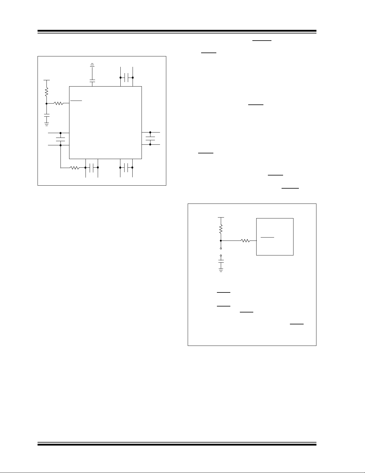
dsPIC33FJXXXGPX06/X08/X10
dsPIC33F
VDD
VSS
VDD
VSS
VSS
VDD
AVDD
AVSS
VDD
VSS
0.1 µF
Ceramic
0.1 µF
Ceramic
0.1 µF
Ceramic
0.1 µF
Ceramic
C
R
V
DD
MCLR
0.1 µF
Ceramic
VCAP/VDDCORE
10 Ω
R1
Note 1: R ≤ 10 kΩ is recommended. A suggested
starting value is 10 kΩ. Ensure that the
MCLR
pin VIH and VIL specifications are met.
2: R1 ≤ 470Ω will limit any current flowing into
MCLR
from the external capacitor C, in the
event of MCLR
pin breakdown, due to
Electrostatic Discharge (ESD) or Electrical
Overstress (EOS). Ensure that the MCLR
pin
V
IH and VIL specifications are met.
C
R1
R
V
DD
MCLR
dsPIC33F
JP
FIGURE 2-1: RECOMMENDED
MINIMUM CONNECTION
2.2.1 TANK CAPACITORS
On boards with power traces running longer than six
inches in length, it is suggested to use a tank capacitor
for integrated circuits including DSCs to supply a local
power source. The value of the tank capacitor should
be determined based on the trace resistance that connects the power supply source to the device, and the
maximum current drawn by the device in the application. In other words, select the tank capacitor so that it
meets the acceptable voltage sag at the device. Typical
values range from 4.7 µF to 47 µF.
2.4 Master Clear (MCLR) Pin
The MCLR pin provides for two specific device
functions:
• Device Reset
• Device programming and debugging
During device programming and debugging, the
resistance and capacitance that can be added to the
pin must be considered. Device programmers and
debuggers drive the MCLR
specific voltage levels (VIH and VIL) and fast signal
transitions must not be adversely affected. Therefore,
specific values of R and C will need to be adjusted
based on the application and PCB requirements.
For example, as shown in Figure 2-2, it is
recommended that the capacitor C, be isolated from
the MCLR
pin during programming and debugging
operations.
Place the components shown in Figure 2-2 within
one-quarter inch (6 mm) from the MCLR
FIGURE 2-2: EXAMPLE OF MCLR PIN
CONNECTIONS
pin. Consequently,
pin.
2.3 Capacitor on Internal Voltage
Regulator (V
A low-ESR (< 5 Ohms) capacitor is required on the
CAP/VDDCORE pin, which is used to stabilize the
V
voltage regulator output voltage. The V
pin must not be connected to VDD, and must have a
capacitor between 4.7 µF and 10 µF, 16V connected to
ground. The type can be ceramic or tantalum. Refer to
Section 25.0 “Electrical Characteristics” for
additional information.
The placement of this capacitor should be close to the
CAP/VDDCORE. It is recommended that the trace
V
length not exceed one-quarter inch (6 mm). Refer to
Section 22.2 “On-Chip Voltage Regulator” for
details.
DS70286C-page 18 © 2009 Microchip Technology Inc.
CAP/VDDCORE)
CAP/VDDCORE
dsPIC33FJXXXGPX06/X08/X10
13
Main Oscillator
Guard Ring
Guard Trace
Secondary
Oscillator
14
15
16
17
18
19
20
2.5 ICSP Pins
The PGECx and PGEDx pins are used for In-Circuit
Serial Programming™ (ICSP™) and debugging purposes. It is recommended to keep the trace length
between the ICSP connector and the ICSP pins on the
device as short as possible. If the ICSP connector is
expected to experience an ESD event, a series resistor
is recommended, with the value in the range of a few
tens of Ohms, not to exceed 100 Ohms.
Pull-up resistors, series diodes, and capacitors on the
PGECx and PGEDx pins are not recommended as they
will interfere with the programmer/debugger communications to the device. If such discrete components are
an application requirement, they should be removed
from the circuit during programming and debugging.
Alternatively, refer to the AC/DC characteristics and
timing requirements information in the respective
device Flash programming specification for information
on capacitive loading limits and pin input voltage high
IH) and input low (VIL) requirements.
(V
Ensure that the “Communication Channel Select” (i.e.,
PGECx/PGEDx pins) programmed into the device
matches the physical connections for the ICSP to
®
MPLAB
ICE™.
For more information on ICD 2, ICD 3 and REAL ICE
connection requirements, refer to the following
documents that are available on the Microchip website.
• “MPLAB
• “Using MPLAB
• “MPLAB
• “Using MPLAB
• “MPLAB
• “MPLAB
• “Using MPLAB
ICD 2, MPLAB ICD 3, or MPLAB REAL
®
ICD 2 In-Circuit Debugger User’s
Guide” DS51331
®
®
ICD 2” (poster) DS51265
ICD 2 Design Advisory” DS51566
®
ICD 3 In-Circuit Debugger”
(poster) DS51765
®
ICD 3 Design Advisory” DS51764
®
REAL ICE™ In-Circuit Emulator User’s
Guide” DS51616
®
REAL ICE™” (poster) DS51749
2.6 External Oscillator Pins
Many DSCs have options for at least two oscillators: a
high-frequency primary oscillator and a low-frequency
secondary oscillator (refer to Section 9.0 “Oscillator
Configuration” for details).
The oscillator circuit should be placed on the same
side of the board as the device. Also, place the
oscillator circuit close to the respective oscillator pins,
not exceeding one-half inch (12 mm) distance
between them. The load capacitors should be placed
next to the oscillator itself, on the same side of the
board. Use a grounded copper pour around the
oscillator circuit to isolate them from surrounding
circuits. The grounded copper pour should be routed
directly to the MCU ground. Do not run any signal
traces or power traces inside the ground pour. Also, if
using a two-sided board, avoid any traces on the
other side of the board where the crystal is placed. A
suggested layout is shown in Figure 2-3.
FIGURE 2-3: SUGGESTED PLACEMENT
OF THE OSCILLATOR
CIRCUIT
© 2009 Microchip Technology Inc. DS70286C-page 19

dsPIC33FJXXXGPX06/X08/X10
2.7 Oscillator Value Conditions on Device Start-up
If the PLL of the target device is enabled and
configured for the device start-up oscillator, the
maximum oscillator source frequency must be limited
to 4 MHz < F
start-up conditions. This means that if the external
oscillator frequency is outside this range, the
application must start-up in the FRC mode first. The
default PLL settings after a POR with an oscillator
frequency outside this range will violate the device
operating speed.
Once the device powers up, the application firmware
can initialize the PLL SFRs, CLKDIV and PLLDBF to a
suitable value, and then perform a clock switch to the
Oscillator + PLL clock source. Note that clock switching
must be enabled in the device Configuration word.
2.8 Configuration of Analog and
IN < 8 MHz to comply with device PLL
Digital Pins During ICSP
Operations
If MPLAB ICD 2, ICD 3 or REAL ICE is selected as a
debugger, it automatically initializes all of the A/D input
pins (ANx) as “digital” pins, by setting all bits in the
ADPCFG and ADPCFG2 registers.
The bits in the registers that correspond to the A/D pins
that are initialized by MPLAB ICD 2, ICD 3, or REAL
ICE, must not be cleared by the user application
firmware; otherwise, communication errors will result
between the debugger and the device.
If your application needs to use certain A/D pins as
analog input pins during the debug session, the user
application must clear the corresponding bits in the
ADPCFG and ADPCFG2 registers during initialization
of the ADC module.
When MPLAB ICD 2, ICD 3 or REAL ICE is used as a
programmer, the user application firmware must
correctly configure the ADPCFG and ADPCFG2
registers. Automatic initialization of these registers is
only done during debugger operation. Failure to
correctly configure the register(s) will result in all A/D
pins being recognized as analog input pins, resulting in
the port value being read as a logic ‘0’, which may
affect user application functionality.
2.9 Unused I/Os
Unused I/O pins should be configured as outputs and
driven to a logic-low state.
Alternatively, connect a 1k to 10k resistor to V
unused pins and drive the output to logic low.
DS70286C-page 20 © 2009 Microchip Technology Inc.
SS on

dsPIC33FJXXXGPX06/X08/X10
3.0 CPU
Note: This data sheet summarizes the features
of the dsPIC33FJXXXGPX06/X08/X10
family of devices. However, it is not
intended to be a comprehensive reference
source. To complement the information in
this data sheet, refer to Section 2. “CPU”
(DS70204) in the “dsPIC33F Family Ref-
erence Manual”, which is available from
the Microchip web site
(www.microchip.com).
The dsPIC33FJXXXGPX06/X08/X10 CPU module has a
16-bit (data) modified Harvard architecture with an
enhanced instruction set, including significant support for
DSP. The CPU has a 24-bit instruction word with a variable
length opcode field. The Program Counter (PC) is 23 bits
wide and addresses up to 4M x 24 bits of user program
memory space. The actual amount of program memory
implemented varies by device. A single-cycle instruction
prefetch mechanism is used to help maintain throughput
and provides predictable execution. All instructions execute
in a single cycle, with the exception of instructions that
MOV.D
DO
)
and
change the program flow, the double word move (
instruction and the table instructions. Overhead-free program loop constructs are supported using the
REPEAT
point.
The dsPIC33FJXXXGPX06/X08/X10 devices have sixteen,
16-bit working registers in the programmer’s model. Each of
the working registers can serve as a data, address or
address offset register. The 16th working register (W15)
operates as a software Stack Pointer (SP) for interrupts and
calls.
The dsPIC33FJXXXGPX06/X08/X10 instruction set has
two classes of instructions: MCU and DSP. These two
instruction classes are seamlessly integrated into a single
CPU. The instruction set includes many addressing modes
and is designed for optimum C compiler efficiency. For most
instructions, the dsPIC33FJXXXGPX06/X08/X10 is capable of executing a data (or program data) memory read, a
working register (data) read, a data memory write and a
program (instruction) memory read per instruction cycle. As
a result, three parameter instructions can be supported,
allowing A + B = C operations to be executed in a single
cycle.
A block diagram of the CPU is shown in Figure 3-1. The
programmer’s model for the
dsPIC33FJXXXGPX06/X08/X10 is shown in Figure 3-2.
instructions, both of which are interruptible at any
3.1 Data Addressing Overview
The data space can be addressed as 32K words or
64 Kbytes and is split into two blocks, referred to as X and
Y data memory. Each memory block has its own independent Address Generation Unit (AGU). The MCU class of
instructions operates solely through the X memory AGU,
which accesses the entire memory map as one linear data
space. Certain DSP instructions operate through the X and
Y AGUs to support dual operand reads, which splits the
data address space into two parts. The X and Y data space
boundary is device-specific.
Overhead-free circular buffers (Modulo Addressing mode)
are supported in both X and Y address spaces. The Modulo
Addressing removes the software boundary checking overhead for DSP algorithms. Furthermore, the X AGU circular
addressing can be used with any of the MCU class of
instructions. The X AGU also supports Bit-Reversed
Addressing to greatly simplify input or output data
reordering for radix-2 FFT algorithms.
The upper 32 Kbytes of the data space memory map can
optionally be mapped into program space at any 16K program word boundary defined by the 8-bit Program Space
Visibility Page (PSVPAG) register. The program to data
space mapping feature lets any instruction access program
space as if it were data space. The data space also includes
2 Kbytes of DMA RAM, which is primarily used for DMA
data transfers, but may be used as general purpose RAM.
3.2 DSP Engine Overview
The DSP engine features a high-speed, 17-bit by 17-bit
multiplier, a 40-bit ALU, two 40-bit saturating accumulators and a 40-bit bidirectional barrel shifter. The barrel
shifter is capable of shifting a 40-bit value, up to 16 bits
right or left, in a single cycle. The DSP instructions operate
seamlessly with all other instructions and have been
designed for optimal real-time performance. The
instruction and other associated instructions can concurrently fetch two data operands from memory while multiplying two W registers and accumulating and optionally
saturating the result in the same cycle. This instruction
functionality requires that the RAM memory data space be
split for these instructions and linear for all others. Data
space partitioning is achieved in a transparent and flexible
manner through dedicating certain working registers to
each address space.
MAC
3.3 Special MCU Features
The dsPIC33FJXXXGPX06/X08/X10 features a 17-bit by
17-bit, single-cycle multiplier that is shared by both the
MCU ALU and DSP engine. The multiplier can perform
signed, unsigned and mixed-sign multiplication. Using a
17-bit by 17-bit multiplier for 16-bit by 16-bit multiplication
not only allows you to perform mixed-sign multiplication, it
also achieves accurate results for special operations,
such as (-1.0) x (-1.0).
The dsPIC33FJXXXGPX06/X08/X10 supports 16/16 and
32/16 divide operations, both fractional and integer. All
divide instructions are iterative operations. They must be
executed within a
tion time of 19 instruction cycles. The divide operation can
be interrupted during any of those 19 cycles without loss
of data.
A 40-bit barrel shifter is used to perform up to a 16-bit, left
or right shift in a single cycle. The barrel shifter can be used
by both MCU and DSP instructions.
REPEAT
loop, resulting in a total execu-
© 2009 Microchip Technology Inc. DS70286C-page 21
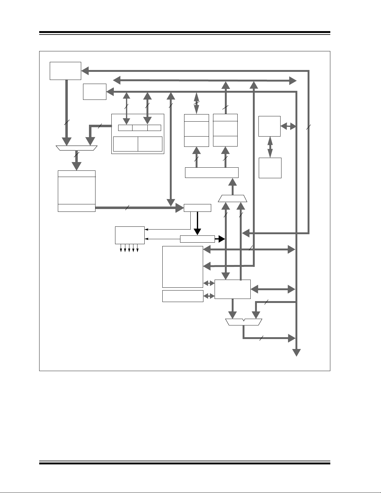
Instruction
Decode and
Control
PCH PCL
Program Counter
16-bit ALU
24
23
Instruction Reg
PCU
16 x 16
W Register Array
ROM Latch
EA MUX
Interrupt
Controller
Stac k
Control
Logic
Loop
Control
Logic
Data Latch
Address
Latch
Control Signals
to Various Blocks
Literal Data
16
16
16
To Peripheral Modules
Data Latch
Address
Latch
16
X RAM
Y RAM
Address Generator Units
16
Y Data Bus
X Data Bus
DMA
Controller
DMA
RAM
DSP Engine
Divide Support
16
16
23
23
16
8
PSV and Table
Data Access
Control Block
16
16
16
16
Program Memory
Data Latch
Address Latch
dsPIC33FJXXXGPX06/X08/X10
FIGURE 3-1: dsPIC33FJXXXGPX06/X08/X10 CPU CORE BLOCK DIAGRAM
DS70286C-page 22 © 2009 Microchip Technology Inc.
dsPIC33FJXXXGPX06/X08/X10
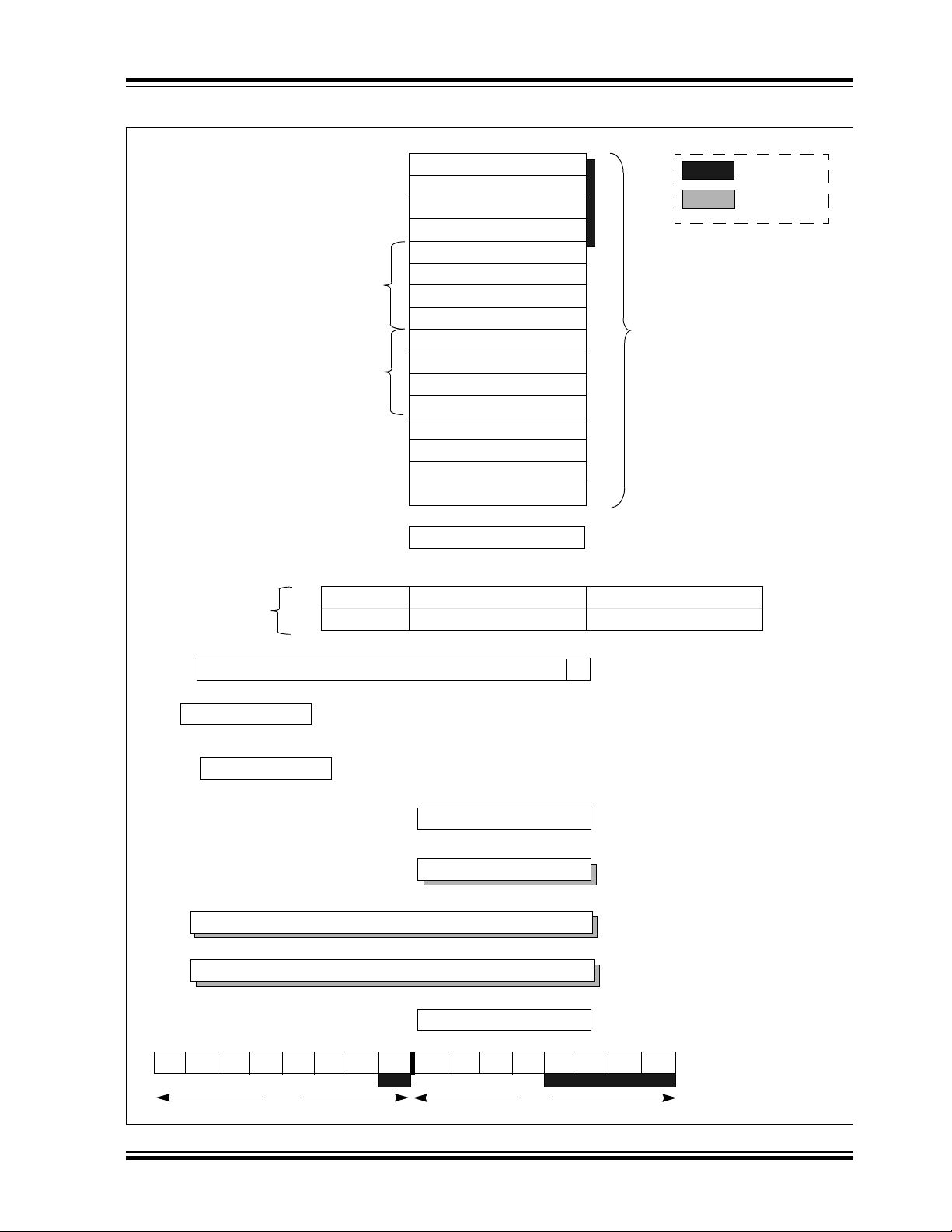
PC22
PC0
7
0
D0D15
Program Counter
Data Table Page Address
STATUS Register
Working Registers
DSP Operand
Registers
W1
W2
W3
W4
W5
W6
W7
W8
W9
W10
W11
W12/DSP Offset
W13/DSP Write Back
W14/Frame Pointer
W15/Stack Pointer
DSP Address
Registers
AD39 AD0AD31
DSP
Accumulators
AccA
AccB
7
0
Program Space Visibility Page Address
Z
0
OA OB SA SB
RCOUNT
15
0
REPEAT Loop Counter
DCOUNT
15
0
DO Loop Counter
DOSTART
22
0
DO Loop Start Address
IPL2 IPL1
SPLIM
Stack Pointer Limit Register
AD15
SRL
PUSH.S Shadow
DO Shadow
OAB SAB
15
0
Core Configuration Register
Legend
CORCON
DA DC
RA
N
TBLPAG
PSVPAG
IPL0 OV
W0/WREG
SRH
DO Loop End Address
DOEND
22
C
FIGURE 3-2: dsPIC33FJXXXGPX06/X08/X10 PROGRAMMER’S MODEL
© 2009 Microchip Technology Inc. DS70286C-page 23
dsPIC33FJXXXGPX06/X08/X10
3.4 CPU Control Registers
CPU control registers include:
• SR: CPU STATUS REGISTER
• CORCON: CORE CONTROL REGISTER
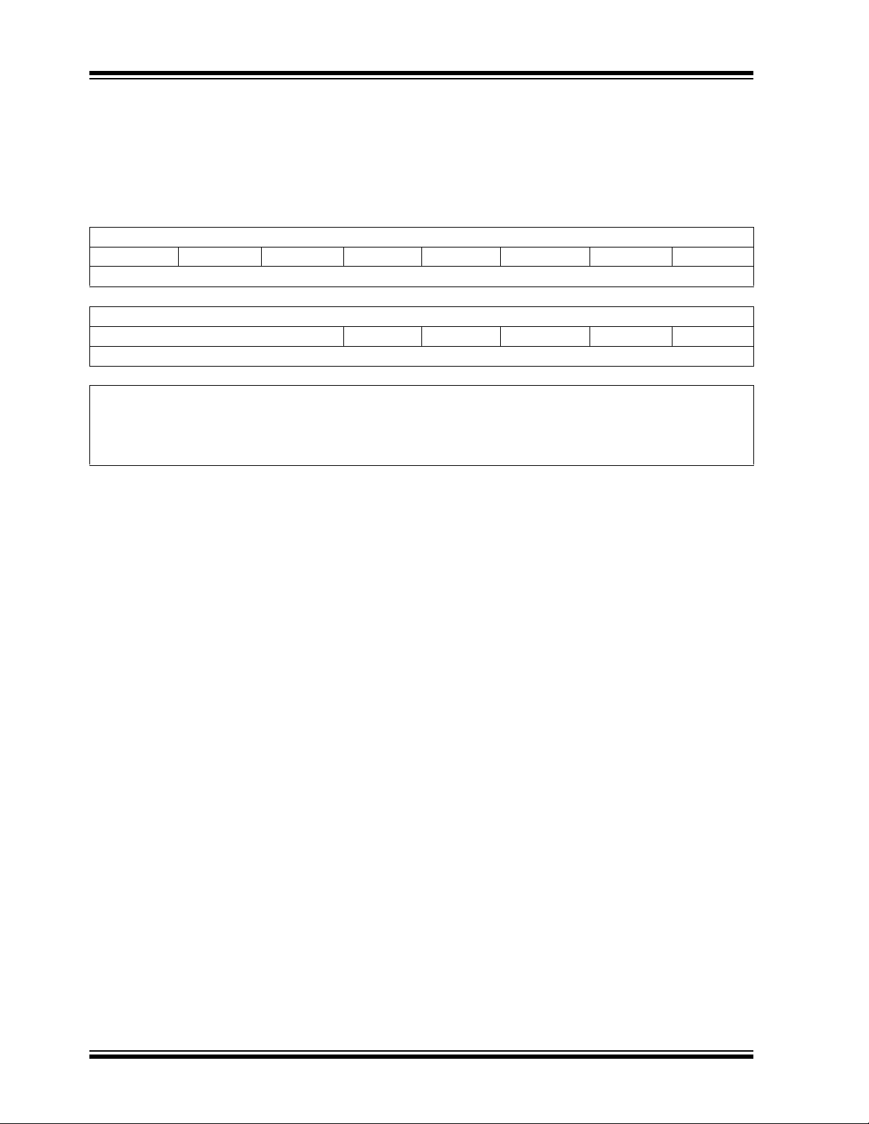
REGISTER 3-1: SR: CPU STATUS REGISTER
R-0 R-0 R/C-0 R/C-0 R-0 R/C-0 R -0 R/W-0
OA OB SA
(1)
bit 15 bit 8
SB
(1)
OAB SAB DA DC
R/W-0
(2)
IPL<2:0>
R/W-0
(3)
(2)
R/W-0
(3)
R-0 R/W-0 R/W-0 R/W-0 R/W-0
RA N OV Z C
bit 7 bit 0
Legend:
C = Clear only bit R = Readable bit U = Unimplemented bit, read as ‘0’
S = Set only bit W = Writable bit -n = Value at POR
‘1’ = Bit is set ‘0’ = Bit is cleared x = Bit is unknown
bit 15 OA: Accumulator A Overflow Status bit
1 = Accumulator A overflowed
0 = Accumulator A has not overflowed
bit 14 OB: Accumulator B Overflow Status bit
1 = Accumulator B overflowed
0 = Accumulator B has not overflowed
bit 13 SA: Accumulator A Saturation ‘Sticky’ Status bit
(1)
1 = Accumulator A is saturated or has been saturated at some time
0 = Accumulator A is not saturated
bit 12 SB: Accumulator B Saturation ‘Sticky’ Status bit
(1)
1 = Accumulator B is saturated or has been saturated at some time
0 = Accumulator B is not saturated
bit 11 OAB: OA || OB Combined Accumulator Overflow Status bit
1 = Accumulators A or B have overflowed
0 = Neither Accumulators A or B have overflowed
bit 10 SAB: SA || SB Combined Accumulator ‘Sticky’ Status bit
1 = Accumulators A or B are saturated or have been saturated at some time in the past
0 = Neither Accumulator A or B are saturated
Note: This bit may be read or cleared (not set). Clearing this bit will clear SA and SB.
bit 9 DA: DO Loop Active bit
1 = DO loop in progress
0 = DO loop not in progress
Note 1: This bit may be read or cleared (not set).
2: The IPL<2:0> bits are concatenated with the IPL<3> bit (CORCON<3>) to form the CPU Interrupt Priority
Level. The value in parentheses indicates the IPL if IPL<3> = 1. User interrupts are disabled when
IPL<3> = 1.
3: The IPL<2:0> Status bits are read only when NSTDIS = 1 (INTCON1<15>).
DS70286C-page 24 © 2009 Microchip Technology Inc.

dsPIC33FJXXXGPX06/X08/X10
REGISTER 3-1: SR: CPU STATUS REGISTER (CONTINUED)
bit 8 DC: MCU ALU Half Carry/Borrow bit
1 = A carry-out from the 4th low-order bit (for byte sized data) or 8th low-order bit (for word sized data)
of the result occurred
0 = No carry-out from the 4th low-order bit (for byte sized data) or 8th low-order bit (for word sized
data) of the result occurred
bit 7-5 IPL<2:0>: CPU Interrupt Priority Level Status bits
111 = CPU Interrupt Priority Level is 7 (15), user interrupts disabled
110 = CPU Interrupt Priority Level is 6 (14)
101 = CPU Interrupt Priority Level is 5 (13)
100 = CPU Interrupt Priority Level is 4 (12)
011 = CPU Interrupt Priority Level is 3 (11)
010 = CPU Interrupt Priority Level is 2 (10)
001 = CPU Interrupt Priority Level is 1 (9)
000 = CPU Interrupt Priority Level is 0 (8)
bit 4 RA: REPEAT Loop Active bit
1 = REPEAT loop in progress
0 = REPEAT loop not in progress
bit 3 N: MCU ALU Negative bit
1 = Result was negative
0 = Result was non-negative (zero or positive)
bit 2 OV: MCU ALU Overflow bit
This bit is used for signed arithmetic (2’s complement). It indicates an overflow of the magnitude which
causes the sign bit to change state.
1 = Overflow occurred for signed arithmetic (in this arithmetic operation)
0 = No overflow occurred
bit 1 Z: MCU ALU Zero bit
1 = An operation which affects the Z bit has set it at some time in the past
0 = The most recent operation which affects the Z bit has cleared it (i.e., a non-zero result)
bit 0 C: MCU ALU Carry/Borrow
1 = A carry-out from the Most Significant bit of the result occurred
0 = No carry-out from the Most Significant bit of the result occurred
Note 1: This bit may be read or cleared (not set).
2: The IPL<2:0> bits are concatenated with the IPL<3> bit (CORCON<3>) to form the CPU Interrupt Priority
Level. The value in parentheses indicates the IPL if IPL<3> = 1. User interrupts are disabled when
IPL<3> = 1.
3: The IPL<2:0> Status bits are read only when NSTDIS = 1 (INTCON1<15>).
bit
(2)
© 2009 Microchip Technology Inc. DS70286C-page 25
dsPIC33FJXXXGPX06/X08/X10
REGISTER 3-2: CORCON: CORE CONTROL REGISTER
U-0 U-0 U-0 R/W-0 R/W-0 R-0 R-0 R-0
— — —USEDT
(1)
DL<2:0>
bit 15 bit 8
R/W-0 R/W-0 R/W-1 R/W-0 R/C-0 R/W-0 R/W-0 R/W-0
SATA SATB SATDW ACCSAT IPL3
(2)
PSV RND IF
bit 7 bit 0
Legend: C = Clear only bit
R = Readable bit W = Writable bit -n = Value at POR ‘1’ = Bit is set
0’ = Bit is cleared ‘x = Bit is unknown U = Unimplemented bit, read as ‘0’
bit 15-13 Unimplemented: Read as ‘0’
bit 12 US: DSP Multiply Unsigned/Signed Control bit
1 = DSP engine multiplies are unsigned
0 = DSP engine multiplies are signed
bit 11 EDT: Early DO Loop Termination Control bit
(1)
1 = Terminate executing DO loop at end of current loop iteration
0 = No effect
bit 10-8 DL<2:0>: DO Loop Nesting Level Status bits
111 = 7 DO loops active
•
•
•
001 = 1 DO loop active
000 = 0 DO loops active
bit 7 SATA: AccA Saturation Enable bit
1 = Accumulator A saturation enabled
0 = Accumulator A saturation disabled
bit 6 SATB: AccB Saturation Enable bit
1 = Accumulator B saturation enabled
0 = Accumulator B saturation disabled
bit 5 SATDW: Data Space Write from DSP Engine Saturation Enable bit
1 = Data space write saturation enabled
0 = Data space write saturation disabled
bit 4 ACCSAT: Accumulator Saturation Mode Select bit
1 = 9.31 saturation (super saturation)
0 = 1.31 saturation (normal saturation)
bit 3 IPL3: CPU Interrupt Priority Level Status bit 3
(2)
1 = CPU interrupt priority level is greater than 7
0 = CPU interrupt priority level is 7 or less
bit 2 PSV: Program Space Visibility in Data Space Enable bit
1 = Program space visible in data space
0 = Program space not visible in data space
bit 1 RND: Rounding Mode Select bit
1 = Biased (conventional) rounding enabled
0 = Unbiased (convergent) rounding enabled
bit 0 IF: Integer or Fractional Multiplier Mode Select bit
1 = Integer mode enabled for DSP multiply ops
0 = Fractional mode enabled for DSP multiply ops
Note 1: This bit will always read as ‘0’.
2: The IPL3 bit is concatenated with the IPL<2:0> bits (SR<7:5>) to form the CPU interrupt priority level.
DS70286C-page 26 © 2009 Microchip Technology Inc.

dsPIC33FJXXXGPX06/X08/X10
3.5 Arithmetic Logic Unit (ALU)
The dsPIC33FJXXXGPX06/X08/X10 ALU is 16 bits
wide and is capable of addition, subtraction, bit shifts
and logic operations. Unless otherwise mentioned,
arithmetic operations are 2’s complement in nature.
Depending on the operation, the ALU may affect the
values of the Carry (C), Zero (Z), Negative (N),
Overflow (OV) and Digit Carry (DC) Status bits in the
SR register. The C and DC Status bits operate as Borrow and Digit Borrow bits, respectively, for subtraction
operations.
The ALU can perform 8-bit or 16-bit operations,
depending on the mode of the instruction that is used.
Data for the ALU operation can come from the W
register array, or data memory, depending on the
addressing mode of the instruction. Likewise, output
data from the ALU can be written to the W register array
or a data memory location.
Refer to the “dsPIC30F/33F Programmer’s Reference
Manual” (DS70157) for information on the SR bits
affected by each instruction.
The dsPIC33FJXXXGPX06/X08/X10 CPU
incorporates hardware support for both multiplication
and division. This includes a dedicated hardware
multiplier and support hardware for 16-bit-divisor
division.
3.5.1 MULTIPLIER
Using the high-speed 17-bit x 17-bit multiplier of the DSP
engine, the ALU supports unsigned, signed or mixed-sign
operation in several MCU multiplication modes:
1. 16-bit x 16-bit signed
2. 16-bit x 16-bit unsigned
3. 16-bit signed x 5-bit (literal) unsigned
4. 16-bit unsigned x 16-bit unsigned
5. 16-bit unsigned x 5-bit (literal) unsigned
6. 16-bit unsigned x 16-bit signed
7. 8-bit unsigned x 8-bit unsigned
3.5.2 DIVIDER
The divide block supports 32-bit/16-bit and 16-bit/16-bit
signed and unsigned integer divide operations with the
following data sizes:
1. 32-bit signed/16-bit signed divide
2. 32-bit unsigned/16-bit unsigned divide
3. 16-bit signed/16-bit signed divide
4. 16-bit unsigned/16-bit unsigned divide
The quotient for all divide instructions ends up in W0
and the remainder in W1. 16-bit signed and unsigned
DIV instructions can specify any W register for both the
16-bit divisor (Wn) and any W register (aligned) pair
(W(m + 1):Wm) for the 32-bit dividend. The divide
algorithm takes one cycle per bit of divisor, so both
32-bit/16-bit and 16-bit/16-bit instructions take the
same number of cycles to execute.
3.6 DSP Engine
The DSP engine consists of a high-speed,
17-bit x 17-bit multiplier, a barrel shifter and a 40-bit
adder/subtracter (with two target accumulators, round
and saturation logic).
The dsPIC33FJXXXGPX06/X08/X10 is a single-cycle,
instruction flow architecture; therefore, concurrent
operation of the DSP engine with MCU instruction flow is
not possible. However, some MCU ALU and DSP engine
resources may be used concurrently by the same
instruction (e.g., ED, EDAC).
The DSP engine also has the capability to perform
inherent accumulator-to-accumulator operations which
require no additional data. These instructions are ADD,
SUB and NEG.
The DSP engine has various options selected through
various bits in the CPU Core Control register
(CORCON), as listed below:
1. Fractional or integer DSP multiply (IF).
2. Signed or unsigned DSP multiply (US).
3. Conventional or convergent rounding (RND).
4. Automatic saturation on/off for AccA (SATA).
5. Automatic saturation on/off for AccB (SATB).
6. Automatic saturation on/off for writes to data
memory (SATDW).
7. Accumulator Saturation mode selection (ACCSAT).
Table 3-1 provides a summary of DSP instructions. A
block diagram of the DSP engine is shown in
Figure 3-3.
TABLE 3-1: DSP INSTRUCTIONS
SUMMARY
Instruction
CLR A = 0 Yes
ED A = (x – y)
EDAC A = A + (x – y)
MAC A = A + (x * y) Yes
MAC A = A + x
MOVSAC No change in A Yes
MPY A = x * y No
MPY A = x
MPY.N A = – x * y No
MSC A = A – x * y Yes
Algebraic
Operation
2
2
2
2
ACC Write
Back
No
No
No
No
© 2009 Microchip Technology Inc. DS70286C-page 27
dsPIC33FJXXXGPX06/X08/X10
Zero Backfill
Sign-Extend
Barrel
Shifter
40-bit Accumulator A
40-bit Accumulator B
Round
Logic
X Data Bus
To/From W Array
Adder
Saturate
Negate
32
32
33
16
16
16
16
40
40
40
40
S
a
t
u
r
a
t
e
Y Data Bus
40
Carry/Borrow Out
Carry/Borrow In
16
40
Multiplier/Scaler
17-bit
FIGURE 3-3: DSP ENGINE BLOCK DIAGRAM
DS70286C-page 28 © 2009 Microchip Technology Inc.
 Loading...