

Page 1

HV9921/HV9922/HV9923
3-Pin Switch-Mode LED Lamp Driver ICs
Features
• Constant output current:
- HV9921 – 20mA
- HV9922 – 50mA
- HV9923 – 30mA
• Universal 85 - 264VAC operation
• Fixed off-time buck converter
• Internal 475V power MOSFET
Applications
• Decorative lighting
• Low power lighting fixtures
Description
HV9921/HV9922/HV9923 are pulse-width modulated
(PWM), high-efficiency, LED driver control ICs. They
allow efficient operation of LED strings from voltage
sources ranging up to 400VDC. HV9921/22/23 include
an internal high voltage switching MOSFET controlled
with fixed off-time (T
LED string is driven at constant current, thus providing
constant light output and enhanced reliability. The output current is internally fixed at 20mA for HV9921,
50mA for HV992, and 30mA for HV9923. The peak current control scheme provides good regulation of the
output current throughout the universal AC line voltage
range of 85 to 264VAC or DC input voltage of 20 to
400V.
) of approximately 10s. The
OFF
2014 Microchip Technology Inc. DS20005311A-page 1
Page 2

HV9921/HV9922/HV9923
TO OUR VALUED CUSTOMERS
It is our intention to provide our valued customers with the best documentation possible to ensure successful use of your Microchip
products. To this end, we will continue to improve our publications to better suit your needs. Our publications will be refined and
enhanced as new volumes and updates are introduced.
If you have any questions or comments regarding this publication, please contact the Marketing Communications Department via
E-mail at [email protected]. We welcome your feedback.
Most Current Data Sheet
To obtain the most up-to-date version of this data sheet, please register at our Worldwide Web site at:
http://www.microchip.com
You can determine the version of a data sheet by examining its literature number found on the bottom outside corner of any page.
The last character of the literature number is the version number, (e.g., DS30000000A is version A of document DS30000000).
Errata
An errata sheet, describing minor operational differences from the data sheet and recommended workarounds, may exist for current
devices. As device/documentation issues become known to us, we will publish an errata sheet. The errata will specify the revision
of silicon and revision of document to which it applies.
To determine if an errata sheet exists for a particular device, please check with one of the following:
• Microchip’s Worldwide Web site; http://www.microchip.com
• Your local Microchip sales office (see last page)
When contacting a sales office, please specify which device, revision of silicon and data sheet (include literature number) you are
using.
Customer Notification System
Register on our web site at www.microchip.com to receive the most current information on all of our products.
DS20005311A-page 2 2014 Microchip Technology Inc.
Page 3
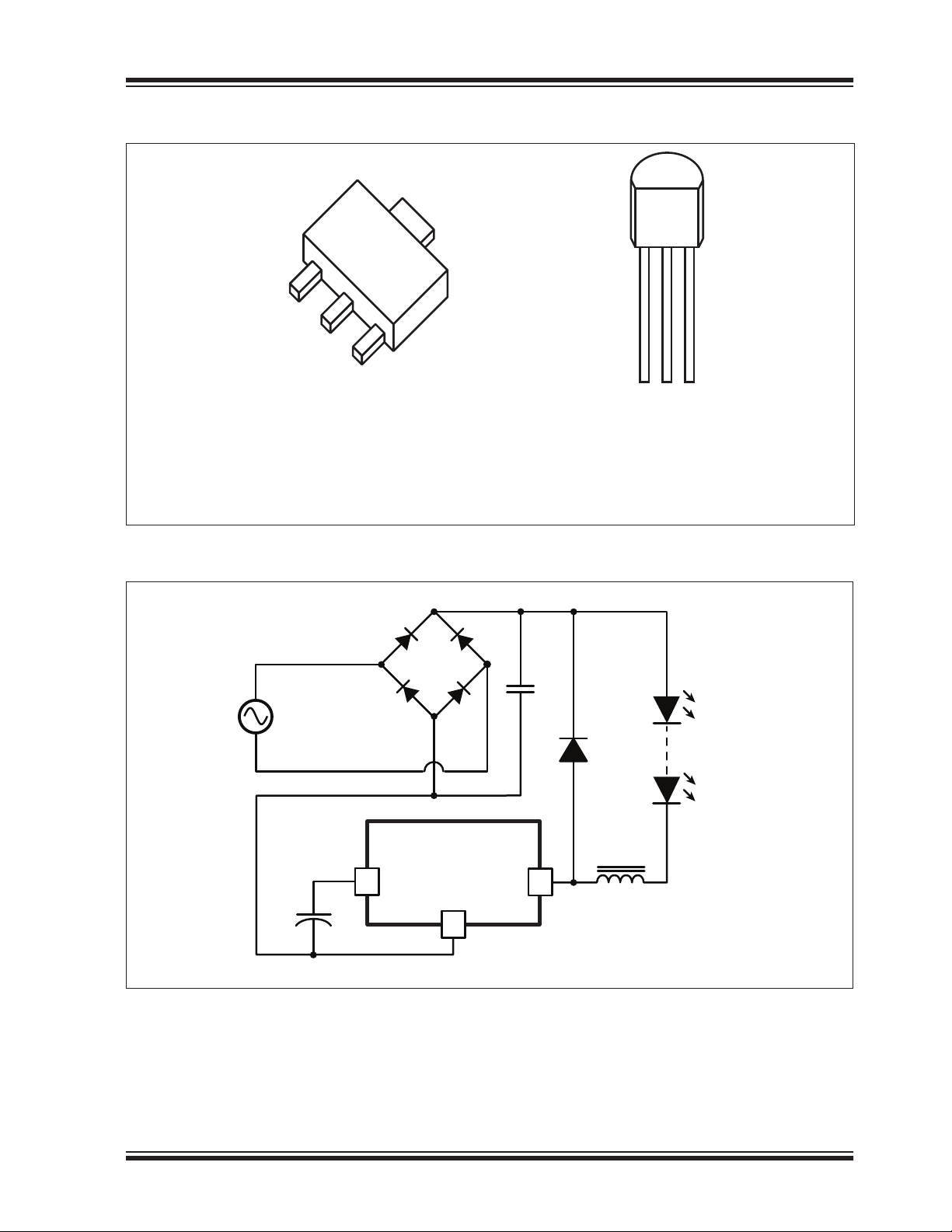
PIN DIAGRAM
1
2
3
(SOT-89)
HV9921/HV9922/HV9923
2
1
3
TO-92TO-243AA
See Table 2-1 for Pin information.
TYPICAL APPLICATION CIRCUIT
AC
HV9921/22/23
3 VDD
GND
2
DRAIN 1
LED
-
LED
1
n
2014 Microchip Technology Inc. DS20005311A-page 3
Page 4
HV9921/HV9922/HV9923
1.0 ELECTRICAL CHARACTERISTICS
ABSOLUTE MAXIMUM RATINGS
Supply Voltage VDD................................ -0.3V to +10V
Supply Current I
Operating Ambient temperature ...........-40°C to +85°C
Operating Junction Temperature ........-40°C to +125°C
Storage temperature ..........................-65°C to +150°C
Power dissipation @+25°C for TO-92 .............740 mW
Power dissipation @+25°C for SOT-89....... 1600 mW*
* Mounted on FR4 board, 24mmx25mmx1.57mm
Note: Stresses above those listed under “Absolute
Maximum Ratings” may cause permanent damage to
the device. This is a stress rating only and functional
operation of the device at those or any other conditions, above those indicated in the operational listings
of this specification, is not implied. Exposure to maximum rating conditions for extended periods may affect
device reliability.
1.1 ELECTRICAL SPECIFICATIONS
..............................................+5mA
DD
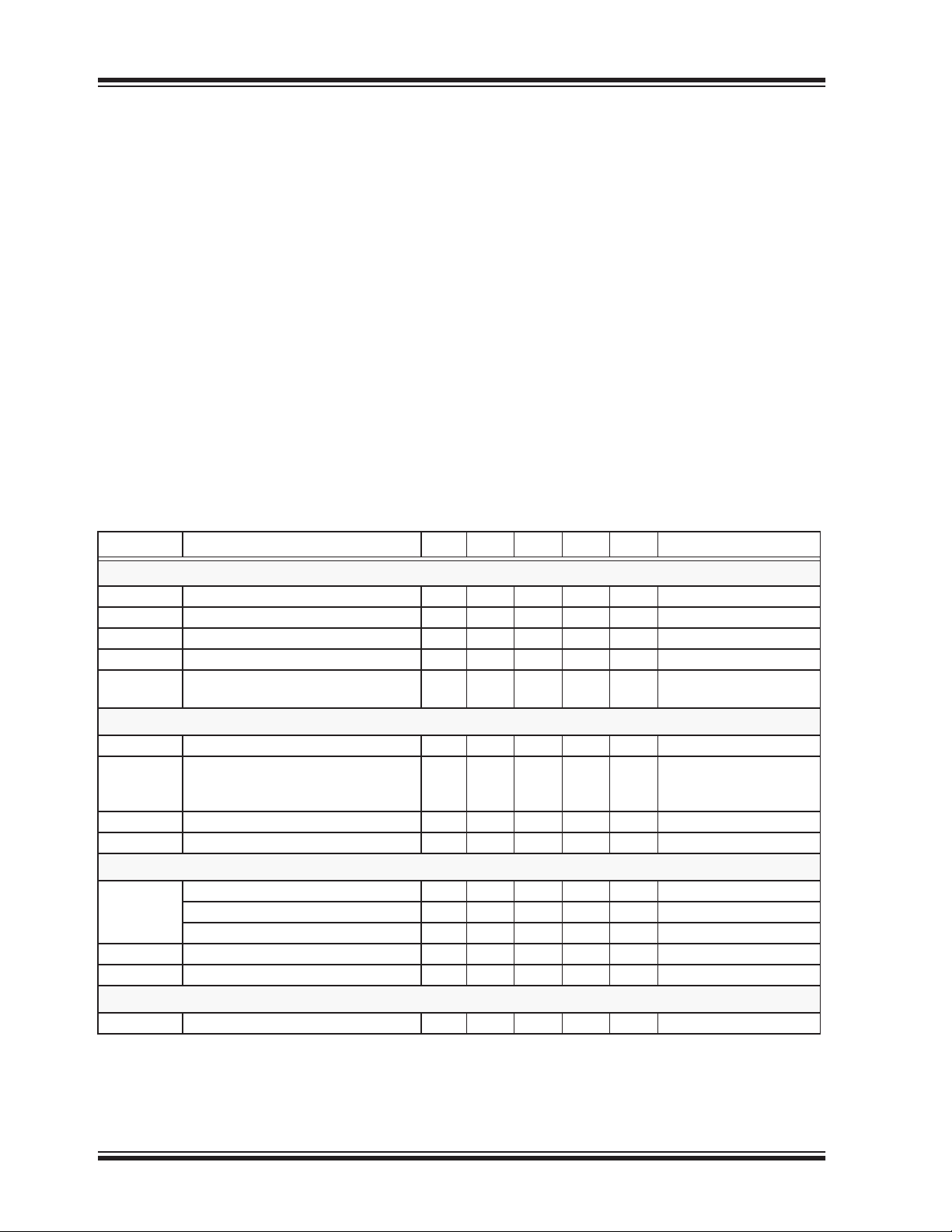
TABLE 1-1: ELECTRICAL CHARACTERISTICS1
Symbol Parameter Notes Min Typ Max Units Conditions
Regulator (VDD)
V
DD
V
DRAIN
V
UVLO
V
UVLO
I
DD
Output (DRAIN)
V
BR
R
ON
C
DRAIN
I
SAT
Current Sense Comparator
I
THL
T
BLANK
T
ON(MIN)
OFF-Time Generator
T
OFF
1 Specifications are T
2 Applies over the full operating ambient temperature range of -40°C < T
3 For design guidance only
V
Regulator Output - - 7.5 - V
DD
V
V
V
Operating Supply Current - - 200 350 A
Breakdown Voltage
ON Resistance - - - 210
Output Capacitance
MOSFET Saturation Current
Threshold Current - HV9921
Threshold Current - HV9922
Threshold Current - HV9923
Leading Edge Blanking Delay
Supply Voltage - 20 - - V
DRAIN
Under-voltage Threshold - 5.0 - - V
DD
Under-voltage Lockout Hysteresis - - 200 - mV
DD
2
475 - - V
3
3
2
2
2
2, 3
-15pFV
100 150 - mA
18.5 - 25.5 mA
49 - 63 mA
28.2 - 38.2 mA
200 300 400 ns
V
DD(EXT)
= 40V
I
DRAIN
I
DRAIN
I
DRAIN
DRAIN
Minimum ON Time - - - 650 ns
OFF Time - 8 10.5 13 S
= 25°C, V
A
= 50V unless otherwise noted.
DRAIN
< +125°C.
A
= 8.5V, V
DRAIN
= 20mA (HV9921)
= 50mA (HV9922)
= 30mA (HV9923)
= 400V
DS20005311A-page 4 2014 Microchip Technology Inc.
Page 5
HV9921/HV9922/HV9923
THERMAL RESISTANCE
Package θja
TO-92 132°C/W
TO-243AA(SOT-89) 133°C/W
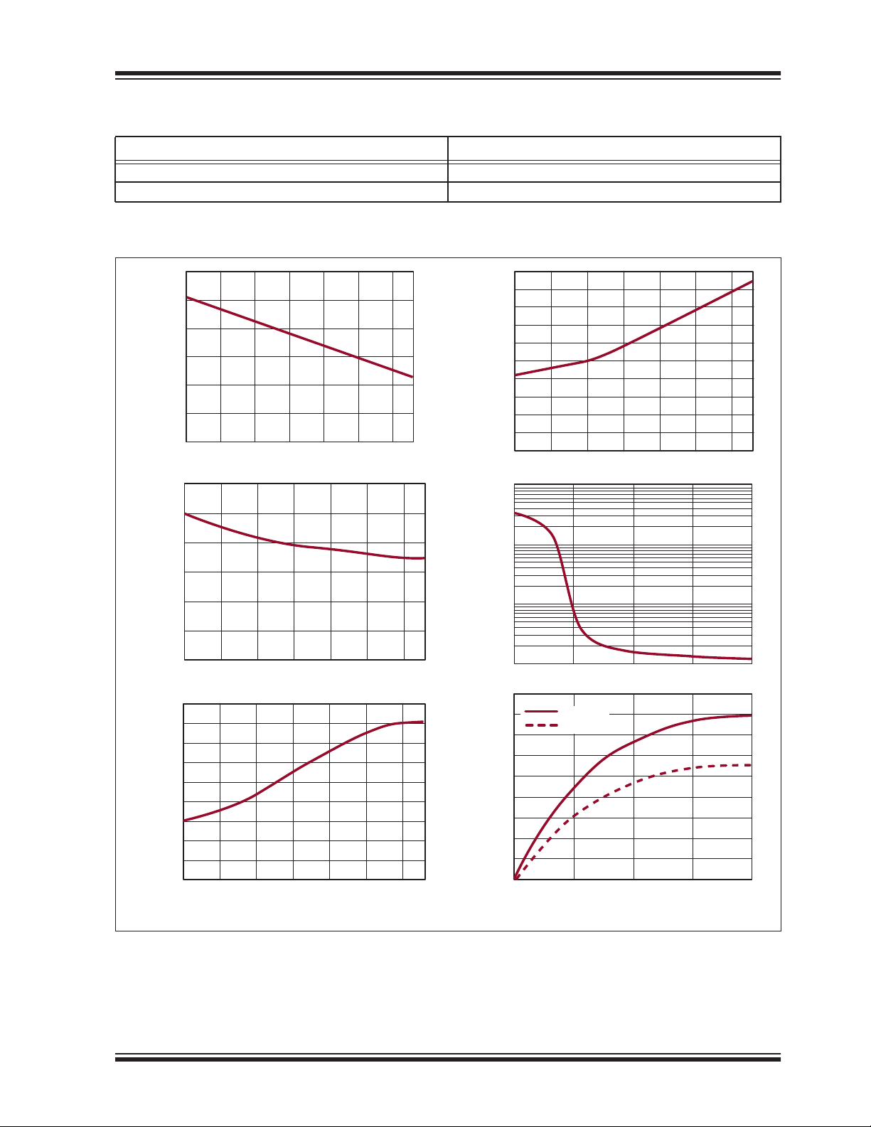
FIGURE 1-1: TYPICAL PERFORMANCE CHARACTERISTICS (TJ= 25°C UNLESS OTHERWISE NOTED)
1.10
1.05
1.00
0.95
0.90
0.85
Normalized Threshold Current
0.80
-40 -15 10 35 60 85 110
Junction Temperature, °C
12
200
180
160
140
120
100
80
60
ON Resistance (μΩ)
40
20
0
-40 -15 10 35 60 85 110
Junction Temperature (°C)
1000
10
8
6
4
OFF Time (μS)
2
0
-40 -15 10 35 60 85 110
Junction Temperature (°C)
580
570
560
550
540
530
520
510
DRAIN Breakdown Voltage (V)
500
490
-40 -15 10 35 60 85 110
Junction Temperature (°C)
100
10
DRAIN Capacitance (pF)
1
0 10 20 30 40
180
160
140
120
100
80
60
DRAIN Current (mA)
40
20
0
0 10 20 30 40
DRAIN Voltage (V)
TJ = 25°C
TJ = 125°C
DRAIN Voltage (V)
2014 Microchip Technology Inc. DS20005311A-page 5
Page 6
HV9921/HV9922/HV9923
2.0 PIN DESCRIPTION
See Pin Diagram on page 3 for the figures.
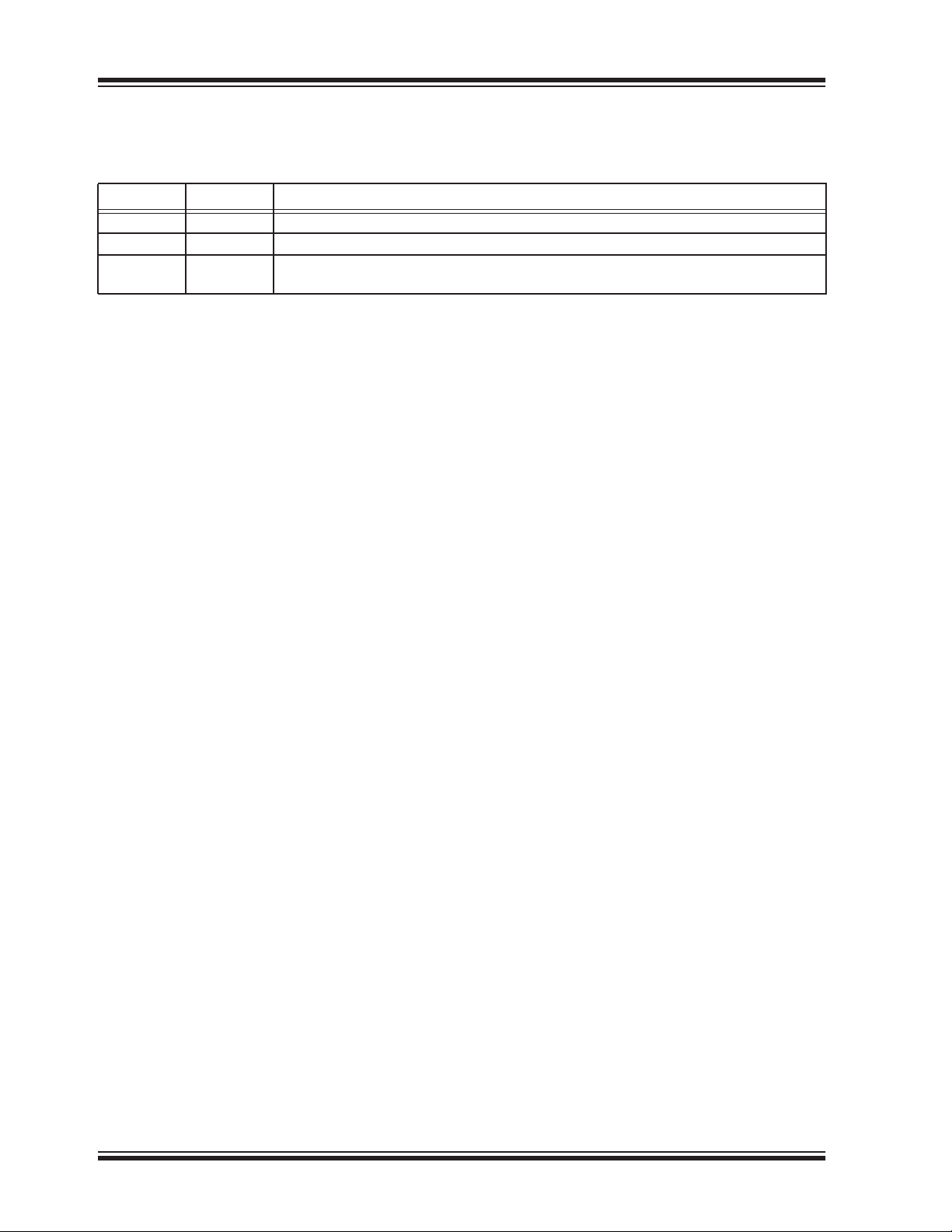
TABLE 2-1: PIN DESCRIPTION
Pin # Name Description
1 Drain Drain terminal of the output switching MOSFET and a linear regulator input
2 GND Common connection for all circuits
3 VDD
Power Supply pin for all control circuits. By pass this pin with a 0.1 F low-impedance
capacitor
3.0 FUNCTIONAL DESCRIPTION
The HV9921/22/23 are PWM peak current controllers
designed to control a buck converter topology in continuous conduction mode (CCM). The output current is
internally preset at 20mA for HV9921, 50mA for
HV992, and 30mA for HV9923.
When the input voltage of 20 to 400V appears at the
DRAIN pin, the internal high-voltage linear regulator
seeks to maintain a voltage of 7.5VDC at the V
Until this voltage exceeds the internally programmed
under-voltage threshold, the output switching MOSFET
is non-conductive. When the threshold is exceeded,
the MOSFET turns on. The input current begins to flow
into the DRAIN pin. Hysteresis is provided in the undervoltage comparator to prevent oscillation.
When the input current exceeds the internal preset
level, a current sense comparator resets an RS flipflop, and the MOSFET turns off. At the same time, a
one-shot circuit is activated that determines the duration of the off-state (10.5s typical). As soon as this
time is over, the flip-flop sets again. The new switching
cycle begins.
A “blanking” delay of 300ns is provided that prevents
false triggering of the current sense comparator due to
the leading edge spike caused by circuit parasitics.
DD
pin.
4.0 APPLICATION INFORMATION
HV9921/22/23 are low-cost off-line buck converter ICs
specifically designed for driving multi-LED strings.
They can be operated from either universal AC line
range of 85 to 264VAC, or 20 to 400VDC, and drive up
to tens of high-brightness LEDs. All LEDs can be run in
series, and the HV9921/22/23 regulate at constant current, yielding uniform illumination. HV9921/22/23 are
compatible with triac dimmers. The output current is
internally fixed at 20mA for HV9921, 50mA for HV9922,
and 30mA for HV9923. These parts are available in
space saving TO-92 and SOT-89 packages.
4.1 Selecting L1 and D1
There is a certain trade-off to be considered between
optimal sizing of the output inductor L1 and the tolerated output current ripple. The required value of L1 is
inversely proportional to the ripple current I
VOT
OFF
------------------------------ -
L1
=
is the forward voltage of the LED string. T
V
O
off-time of HV9921/22/23. The output current in the
LED string (I
where I
The ripple current introduces a peak-to-average error
in the output current setting that needs to be accounted
for. Due to the constant off-time control technique used
in HV9921/22/23, the ripple current is independent of
the input AC or DC line voltage variation. Therefore, the
output current will remain unaffected by the varying
input voltage.
Adding a filter capacitor across the LED string can
reduce the output current ripple even further, thus permitting a reduced value of L1. However, keep in mind
that the peak-to-average current error is affected by the
variation of T
accuracy might be sacrificed at large ripple current in
L1.
Another important aspect of designing an LED driver
with the HV9921/22/23 is related to certain parasitic
elements of the circuit, including distributed coil capacitance of L1, junction capacitance and reverse recovery
of the rectifier diode D1, capacitance of the printed circuit board traces C
of the controller itself. These parasitic elements affect
the efficiency of the switching converter and could
potentially cause false triggering of the current sense
comparator if not properly managed. Minimizing these
parasitics is essential for efficient and reliable operation
of the HV9921/22/23.
) is calculated then as:
O
IOI
is the current sense comparator threshold.
TH
. Therefore, the initial output current
OFF
PCB
IO
1
–=
-- - IO
TH
2
and output capacitance C
in it.
O
OFF
is the
DRAIN
DS20005311A-page 6 2014 Microchip Technology Inc.
Page 7

HV9921/HV9922/HV9923
Coil capacitance of inductors is typically provided in the
manufacturer’s data books either directly or in terms of
the self-resonant frequency (SRF).
=
SRF 1 2 LC
where L is the inductance value, and C
L
is the coil
L
capacitance.) Charging and discharging this capacitance every switching cycle causes high-current spikes
in the LED string. Therefore, connecting a small capacitor C
(~10nF) is recommended to bypass these
O
spikes.
Using an ultra-fast rectifier diode for D1 is recommended to achieve high efficiency and reduce the risk
of false triggering of the current sense comparator.
Using diodes with shorter reverse recovery time, t
and lower junction capacitance, C
performance. The reverse voltage rating, V
, achieves better
J
, of the
R
diode must be greater than the maximum input voltage
of the LED lamp.
The total parasitic capacitance present at the DRAIN
pin of the HV9921/22/23 can be calculated as:
CPC
+++=
DRAINCPCBCLCJ
4.2 Estimating Power Loss
Discharging the parasitic capacitance CP into the
DRAIN pin of the HV9921/22/23 is responsible for the
bulk of the switching power loss. It can be estimated
using the following equation:
2
V
C
IN
P
----------------- - V
2
I
IN
SAT
where F
P
SWITCH
is the switching frequency, I
S
rated DRAIN current of the HV9921/22/23. The switching loss is the greatest at the maximum input voltage.
The switching frequency is given by the following equa-
,
rr
tion.
VINVO–
F
------------------------ -=
S
V
INTOFF
When the HV9921/22/23 LED driver is powered from
the full-wave rectified AC input, the switching power
loss can be estimated as:
P
SWITCH
1
------------------- - V
2T
OFF
ACCP
2I
SATtrr
F
trr+
=
is the satu-
SAT
+VACVO–
S
When the switching MOSFET turns on, the capacitance C
is discharged into the DRAIN pin of the IC.
P
The discharge current is limited to about 150mA typi-
cally. However, it may become lower at increased junction temperature. The duration of the leading edge
current spike can be estimated as:
VINCP
SPIKE
------------------- - trr+=
I
SAT
T
In order to avoid false triggering of the current sense
comparator, C
must be minimized in accordance with
P
the following expression:
where T
BLANK(MIN)
200ns, and V
I
SATTBLANK MINtrr
C
-------------------------------------------------------- -
P
V
IN MAX
is the minimum blanking time of
is the maximum instantaneous
IN(MAX)
–
input voltage.
V
is the input AC line voltage.
AC
The switching power loss associated with turn-off transitions of the DRAIN pin can be disregarded. Due to the
large amount of parasitic capacitance connected to this
switching node, the turn-off transition occurs essentially at zero-voltage.
Conduction power loss in the HV9921/22/23 can be
calculated as:
P
COND
where D = V
tance, I
is the internal linear regulator current.
DD
O/VIN
2
DI
RONIDDVIN1D–+=
O
is the duty ratio, RON is the on-resis-
When the LED driver is powered from the full-wave rectified AC line input, the exact equation for calculating
the conduction loss is more cumbersome. However, it
can be estimated using the following equation:
P
CONDKCIO
where V
K
and Kd can be determined from the minimum duty
C
is the input AC line voltage. The coefficients
AC
2
RONKdIDDVAC+=
ratio of the HV9921/22/23.
2014 Microchip Technology Inc. DS20005311A-page 7
Page 8
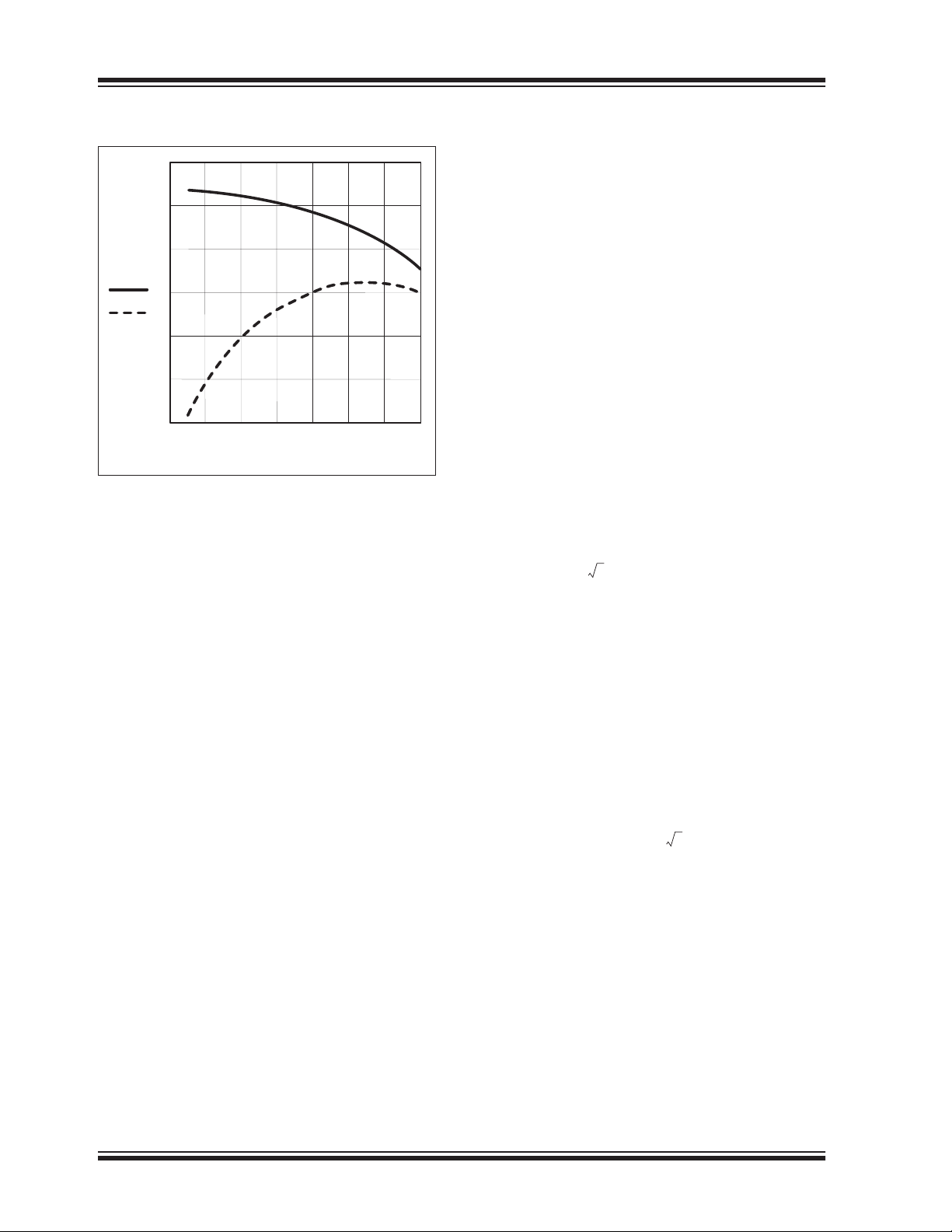
HV9921/HV9922/HV9923
F
FIGURE 4-1: CONDUCTION LOSS
COEFFICIENTS KC AND K
0.7
0.6
0.5
Kd(Dm)
0.4
Kc(Dm)
0.3
0.2
0.1
0 0.1 0.2 0.3 0.4 0.5 0.6 0.7
Dm
4.3 EMI Filter
As with all off-line converters, selecting an input filter is
critical to obtaining good EMI. A switching side capacitor, albeit of small value, is necessary in order to ensure
low impedance to the high frequency switching currents of the converter. As a rule of thumb, this capacitor
should be approximately 0.1-0.2 F/W of LED output
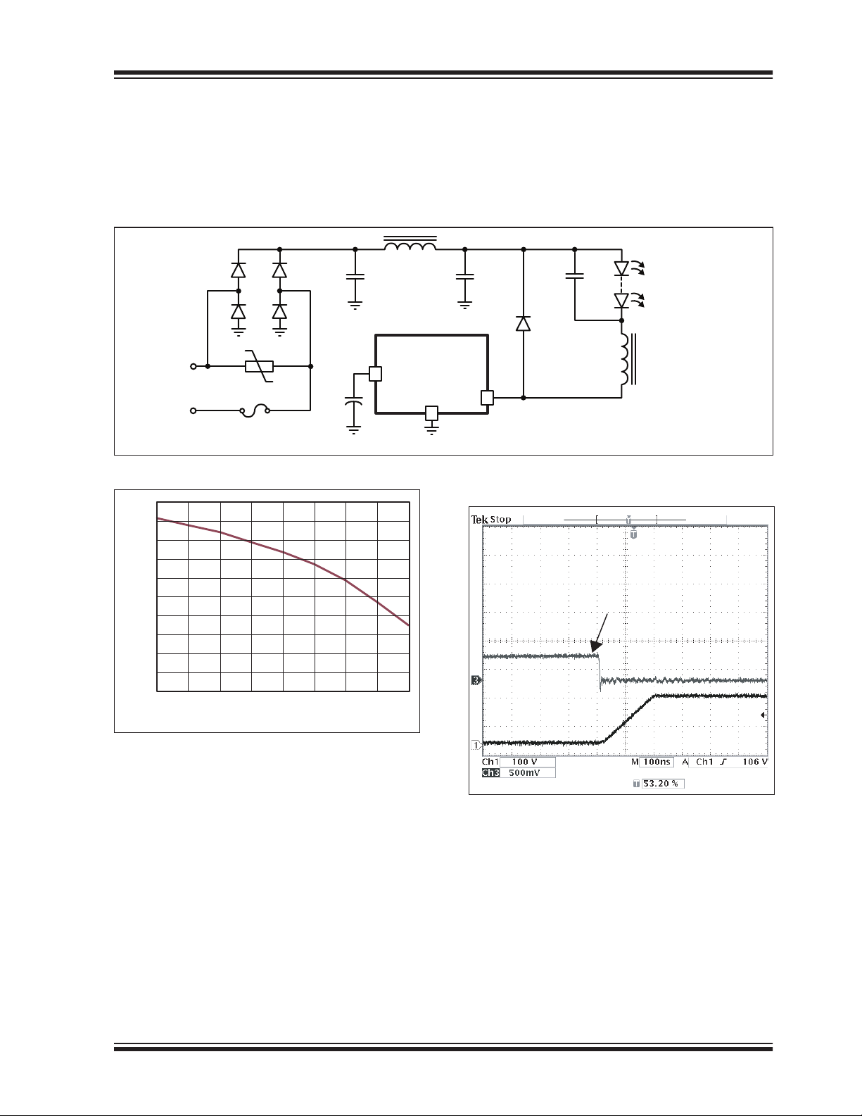
power. A recommended input filter is shown in
Figure 4-2 for the following design example.
Select L1 68mH, I = 30mA. Typical SRF = 170KHz.
d
Calculate the coil capacitance.
C
L
1
----------------------------------------- -
L1 2 SRF
------------------------------------------------------------ - 13p
2
68mH 2 170KHz
1
===
2
4.3.1.2 Step 2. Selecting D1
Usually, the reverse recovery characteristics of ultrafast rectifiers at I
= 20 ~ 50mA are not provided in the
F
manufacturer’s data books. The designer may want to
experiment with different diodes to achieve the best
result.
Select D1 MUR160 with V
20mA, I
= 100mA) and CJ 8pF (VF > 50V).
RR
= 600V, trr 20ns (IF =
R
4.3.1.3 Step 3. Calculating total parasitic
capacitance
5pF 5pF 13pF 8pF 13pF=++ +=
C
p
4.3.1.4 Step 4. Calculating the leading edge
spike duration
T
264V 2 31pF
-------------------------------------------- 20ns 136ns T
SPIKE
100mA
+=
BLANK MIN
4.3.1.5 Step 5. Estimating power dissipation
in HV9921 at 265VAC
4.3.1 DESIGN EXAMPLE
The following example designs a HV9921 LED lamp
driver meeting the following specifications:
• Input: Universal AC, 85-265VAC
• Output Current: 20mA
• Load: String of 10 LED (LW541C by OSRAM VF
= 4.1V max. each)
4.3.1.1 Step 1. Calculating L1.
The output voltage VO = 10 x VF 41V (max.). Use this
equation assuming a 30% peak-to-peak ripple.
41V 10.5s
L1
--------------------------------- - 72mH==
0.3 20mA
Switching power loss:
SWITCH
264V 41V–
-------------------------- 264V 31pF 2 100mA 20ns+
2 10.5s
131mW
P
1
Minimum duty ratio:
M
41V
------------------------- - 0.11=
265V 2
D
Conduction power loss:
P
0.25 20mA
COND
210 0.63 200A 264V
2
55mW
Total power dissipation in HV9921:
P
TOTAL
131mW 55mW 186mW=+=
+=
DS20005311A-page 8 2014 Microchip Technology Inc.
Page 9
HV9921/HV9922/HV9923
4.3.1.6 Step 6. Selecting input capacitor C
IN
OutputPower 41V 20mA 820mW==
Select CIN ECQ-E4104KF by Panasonic® (0.1F,
400V, Metalized Polyester Film).
FIGURE 4-2: UNIVERSAL 85-264VAC LED LAMP DRIVER
L
D2 D3
C
IN2
IN
C
IN
C
O
LED
- LED
1
12
D4 D5
D1
HV9921/22/23
VDD
3
DRAIN
GND
2
L1
1
AC Line
85-265V
VRD1
C
DD
F1
FIGURE 4-3: TYPICAL EFFICIENCY FIGURE 4-4: SWITCH-OFF TRANSITION
82
80
78
76
74
72
70
Efficiency (%)
68
66
64
62
75 100 125 150 175 200 225 250 275
Input AC Line Voltage (VAC)
Ch1:V
ZERO VOLTAGE
TRANSITION
DRAIN
, Ch3: I
DRAIN
2014 Microchip Technology Inc. DS20005311A-page 9
Page 10
HV9921/HV9922/HV9923
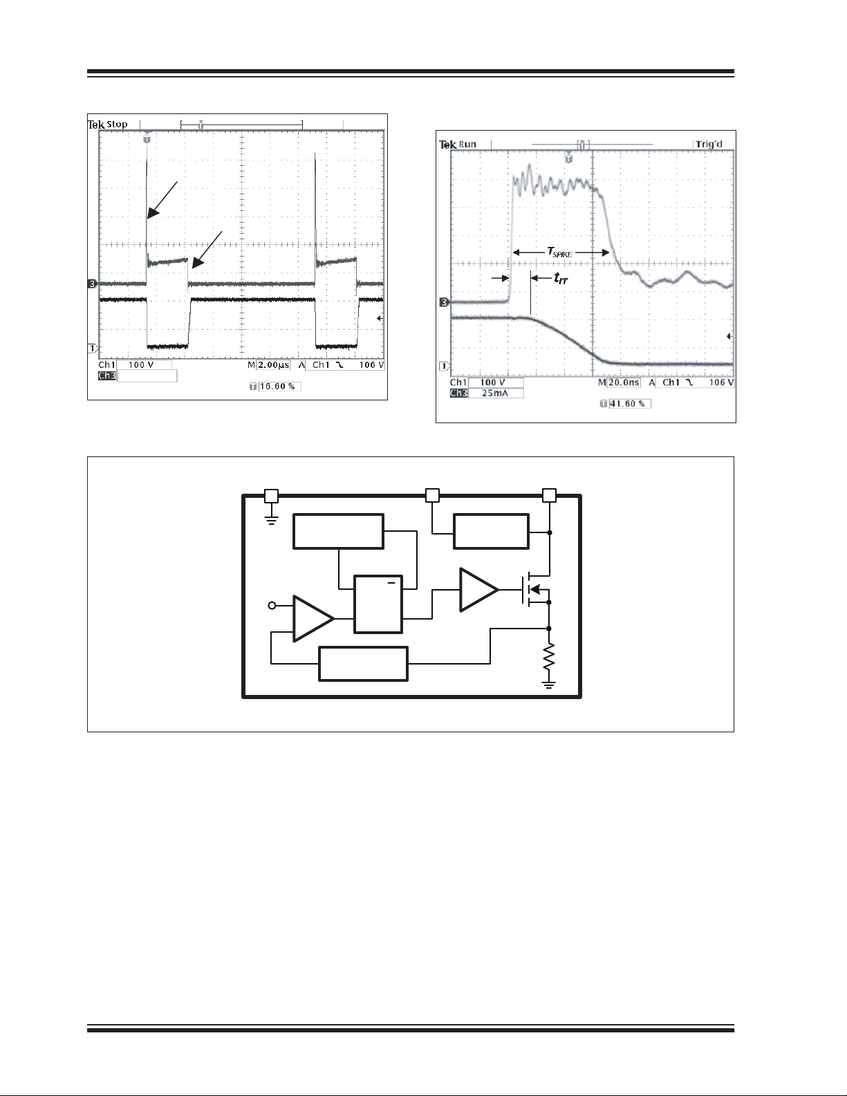
FIGURE 4-5: TYPICAL EFFICIENCY FIGURE 4-6: SWITCH-OFF TRANSITION
Ch1:V
LEADING EDGE SPIKE
SWITCH OFF
25mA
FIGURE 4-7: FUNCTIONAL BLOCK DIAGRAM
DRAIN
, Ch3: I
DRAIN
T
= 10.5μs
OFF
S
REF
-
+
T
BLANK
Q
R
Q
= 300ns
HV9921/HV9922/HV9923
VDD
DRAINGND
Regulator
7.5V
R
DS20005311A-page 10 2014 Microchip Technology Inc.
Page 11
5.0 LAYOUT CONSIDERATIONS
HV9921/HV9922/HV9923
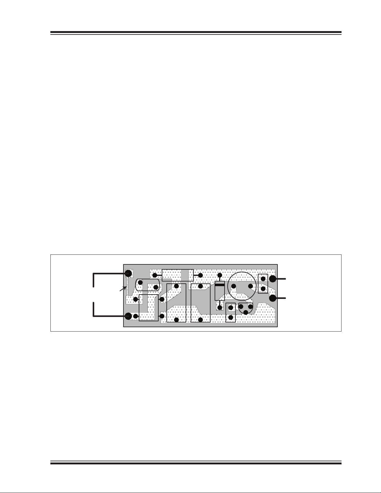
For a recommended circuit board layout for the
HV9921/22/23, see Figure 5-1.
5.1 Single Point Grounding
Use a single point ground connection from the input filter capacitor to the area of copper connected to the
GND pin.
5.2 Bypass Capacitor (CDD)
The VDD pin bypass capacitor CDD should be located
as near as possible to the V
and GND pins.
DD
5.3 Switching Loop Areas
The area of the switching loop connecting the input fil-
ter capacitor C
together should be kept as small as possible.
The switching loop area connecting the output filter
capacitor C
together should be kept as small as possible.
, the diode D1 and the HV9921/22/23
IN
, the inductor L1 and the diode D1
O
5.4 Thermal Considerations vs. Radiated EMI
The copper area where GND pin is connected acts not
only as a single point ground, but also as a heat sink.
This area should be maximized for good heat sinking,
especially when the SOT-89 package is used. The
same applies to the cathode of the free-wheeling diode
D1. Both nodes are quiet; therefore, they will not cause
radiated RF emission. The switching node copper area
connected to the DRAIN pin of the HV9921/22/23, the
anode of D1 and the inductor L1 needs to be minimized. A large switching node area can increase high
frequency radiated EMI.
5.5 Input Filter Layout Considerations
The input circuits of the EMI filter must not be placed in
the direct proximity to the inductor L1 in order to avoid
magnetic coupling of its leakage fields. This consideration is especially important when unshielded construction of L1 is used. When an axial input EMI filter
inductor L
nal with respect to L1. The loop area formed by C
L
and CIN should be minimized. The input lead wires
IN
must be twisted together.
is selected, it must be positioned orthogo-
IN
IN2
,
FIGURE 5-1: RECOMMENDED CIRCUIT BOARD LAYOUT WITH HV9921/22/23
COMPONENT SIDE VIEW
C
O
LED +
LED -
AC Line
85-264VAC
F1
VRD1
D2-5
L
IN
D1
IN2
C
IN
C
DD
C
L1
U1
2014 Microchip Technology Inc. DS20005311A-page 11
Page 12
HV9921/HV9922/HV9923
6.0 PACKAGING INFORMATION
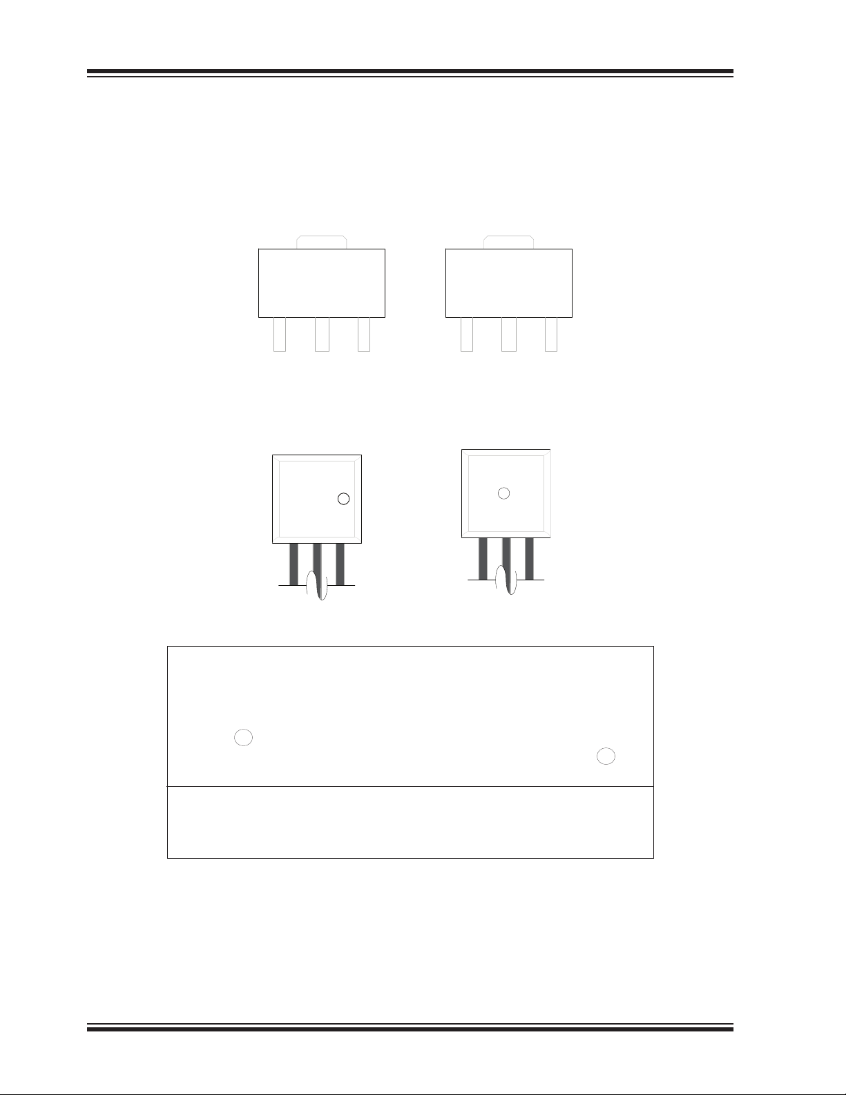
6.1 Package Marking Information
3-lead TO-243AA*
(SOT-89)
XXXYYWW
NNN
3-lead TO-92
XXXXXX
XXXX
YWWNNN
e3
Example
H21YYWW
NNN
Example
HV9921
e3
N3
YWWNNN
Legend: XX...X Product Code or Customer-specific information
Y Year code (last digit of calendar year)
YY Year code (last 2 digits of calendar year)
WW Week code (week of January 1 is week ‘01’)
NNN Alphanumeric traceability code
3
e
Pb-free JEDEC
* This package is Pb-free. The Pb-free JEDEC designator ( )
can be found on the outer packaging for this package.
Note: In the event the full Microchip part number cannot be marked on one line, it will
be carried over to the next line, thus limiting the number of available
characters for product code or customer-specific information. Package may or
may not include the corporate logo.
DS20005311A-page 12 2014 Microchip Technology Inc.
®
designator for Matte Tin (Sn)
3
e
Page 13
HV9921/HV9922/HV9923
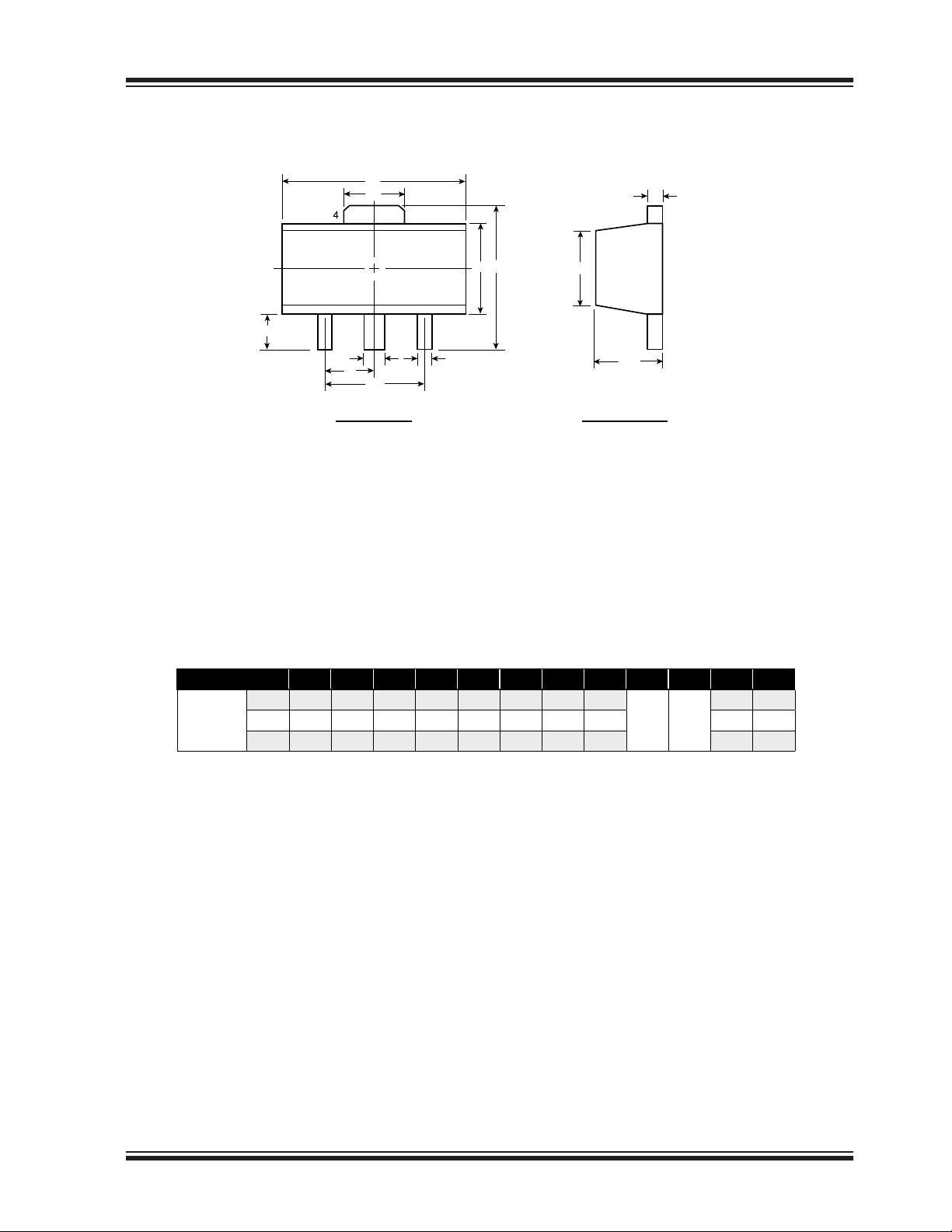
3-Lead TO-243AA (SOT-89) Package Outline (N8)
D
12 3
L
D1
H
E
E1
C
b
e
e1
Top View
Note: For the most current package drawings, see the Microchip Packaging Specification at www.microchip.com/packaging.Note: For the most current package drawings, see the Microchip Packaging Specification at www.microchip.com/packaging.
Symbol A b b1 C D D1 E E1 e e1 H L
Dimensions
(mm)
JEDEC Registration TO-243, Variation AA, Issue C, July 1986.
† This dimension differs from the JEDEC drawing
Drawings not to scale.
MIN 1.40 0.44 0.36 0.35 4.40 1.62 2.29 2.00
NOM-------- --
MAX 1.60 0.56 0.48 0.44 4.60 1.83 2.60 2.29 4.25 1.20
b1
A
Side View
†
1.50
BSC
3.00
BSC
3.94 0.73
†
2014 Microchip Technology Inc. DS20005311A-page 13
Page 14
HV9921/HV9922/HV9923
Note: For the most current package drawings, see the Microchip Packaging Specification at www.microchip.com/packaging.
DS20005311A-page 14 2014 Microchip Technology Inc.
Page 15

APPENDIX A: REVISION HISTORY
Revision A (October 2014)
• Original Release of this Document.
HV9921/HV9922/HV9923
2014 Microchip Technology Inc. DS20005311A-page 15
Page 16

HV9921/HV9922/HV9923
THE MICROCHIP WEB SITE
Microchip provides online support via our WWW site at
www.microchip.com. This web site is used as a means
to make files and information easily available to
customers. Accessible by using your favorite Internet
browser, the web site contains the following
information:
• Product Support – Data sheets and errata,
application notes and sample programs, design
resources, user’s guides and hardware support
documents, latest software releases and archived
software
• General Technical Support – Frequently Asked
Questions (FAQ), technical support requests,
online discussion groups, Microchip consultant
program member listing
• Business of Microchip – Product selector and
ordering guides, latest Microchip press releases,
listing of seminars and events, listings of
Microchip sales offices, distributors and factory
representatives
CUSTOMER CHANGE NOTIFICATION
SERVICE
CUSTOMER SUPPORT
Users of Microchip products can receive assistance
through several channels:
• Distributor or Representative
• Local Sales Office
• Field Application Engineer (FAE)
• Technical Support
Customers should contact their distributor,
representative or Field Application Engineer (FAE) for
support. Local sales offices are also available to help
customers. A listing of sales offices and locations is
included in the back of this document.
Technical support is available through the web site
at: http://microchip.com/support
Microchip’s customer notification service helps keep
customers current on Microchip products. Subscribers
will receive e-mail notification whenever there are
changes, updates, revisions or errata related to a
specified product family or development tool of interest.
To register, access the Microchip web site at
www.microchip.com. Under “Support”, click on
“Customer Change Notification” and follow the
registration instructions.
DS20005311A-page 16 2014 Microchip Technology Inc.
Page 17

HV9921/HV9922/HV9923
PRODUCT IDENTIFICATION SYSTEM
To order or obtain information, e.g., on pricing or delivery, refer to the factory or the listed sales office.
PART NO.
Device
Device: HV9921 = 3-Pin Switch-Mode LED Lamp Driver IC,
Package
Options
-
XX
Environmental
HV9922 = 3-Pin Switch-Mode LED Lamp Driver IC,
HV9923 = 3-Pin Switch-Mode LED Lamp Driver IC,
-
X
20 mA output current
50 mA output current
30 mA output current
X
Reel
Examples:
a) HV9921N3-G: 20 mA output current,
b) HV9923N8-G: 30 mA output current,
TO-92 package, 1000/
bag
TO-243AA(SOT-89)
package, 2000/reel
Package: N3 = TO-92
Environmental G = Lead (Pb)-free/ROHS-compliant package
Reel: (nothing) = 1000/bag for N3 package, 2000/reel for N8
N8 = TO-243AA (SOT-89)
package
2014 Microchip Technology Inc. DS20005311A-page 17
Page 18

Note the following details of the code protection feature on Microchip devices:
• Microchip products meet the specification contained in their particular Microchip Data Sheet.
• Microchip believes that its family of products is one of the most secure families of its kind on the market today, when used in the
intended manner and under normal conditions.
• There are dishonest and possibly illegal methods used to breach the code protection feature. All of these methods, to our
knowledge, require using the Microchip products in a manner outside the operating specifications contained in Microchip’s Data
Sheets. Most likely, the person doing so is engaged in theft of intellectual property.
• Microchip is willing to work with the customer who is concerned about the integrity of their code.
• Neither Microchip nor any other semiconductor manufacturer can guarantee the security of their code. Code protection does not
mean that we are guaranteeing the product as “unbreakable.”
Code protection is constantly evolving. We at Microchip are committed to continuously improving the code protection features of our
products. Attempts to break Microchip’s code protection feature may be a violation of the Digital Millennium Copyright Act. If such acts
allow unauthorized access to your software or other copyrighted work, you may have a right to sue for relief under that Act.
Information contained in this publication regarding device
applications and the like is provided only for your convenience
and may be superseded by updates. It is your responsibility to
ensure that your application meets with your specifications.
MICROCHIP MAKES NO REPRESENTATIONS OR
WARRANTIES OF ANY KIND WHETHER EXPRESS OR
IMPLIED, WRITTEN OR ORAL, STATUTORY OR
OTHERWISE, RELATED TO THE INFORMATION,
INCLUDING BUT NOT LIMITED TO ITS CONDITION,
QUALITY, PERFORMANCE, MERCHANTABILITY OR
FITNESS FOR PURPOSE. Microchip disclaims all liability
arising from this information and its use. Use of Microchip
devices in life support and/or safety applications is entirely at
the buyer’s risk, and the buyer agrees to defend, indemnify and
hold harmless Microchip from any and all damages, claims,
suits, or expenses resulting from such use. No licenses are
conveyed, implicitly or otherwise, under any Microchip
intellectual property rights.
Trademarks
The Microchip name and logo, the Microchip logo, dsPIC,
FlashFlex, KEELOQ, KEELOQ logo, MPLAB, PIC, PICmicro,
PICSTART, PIC32 logo, rfPIC, SST, SST Logo, SuperFlash
and UNI/O are registered trademarks of Microchip
Technology Incorporated in the U.S.A. and other countries.
FilterLab, Hampshire, HI-TECH C, Linear Active Thermistor,
MTP, SEEVAL and The Embedded Control Solutions
Company are registered trademarks of Microchip Technology
Incorporated in the U.S.A.
Silicon Storage Technology is a registered trademark of
Microchip Technology Inc. in other countries.
Analog-for-the-Digital Age, Application Maestro, BodyCom,
chipKIT, chipKIT logo, CodeGuard, dsPICDEM,
dsPICDEM.net, dsPICworks, dsSPEAK, ECAN,
ECONOMONITOR, FanSense, HI-TIDE, In-Circuit Serial
Programming, ICSP, Mindi, MiWi, MPASM, MPF, MPLAB
Certified logo, MPLIB, MPLINK, mTouch, Omniscient Code
Generation, PICC, PICC-18, PICDEM, PICDEM.net, PICkit,
PICtail, REAL ICE, rfLAB, Select Mode, SQI, Serial Quad I/O,
Total Endurance, TSHARC, UniWinDriver, WiperLock, ZENA
and Z-Scale are trademarks of Microchip Technology
Incorporated in the U.S.A. and other countries.
SQTP is a service mark of Microchip Technology Incorporated
in the U.S.A.
GestIC and ULPP are registered trademarks of Microchip
Technology Germany II GmbH & Co. KG, a subsidiary of
Microchip Technology Inc., in other countries.
All other trademarks mentioned herein are property of their
respective companies.
© 2014, Microchip Technology Incorporated, Printed in the
U.S.A., All Rights Reserved.
Printed on recycled paper.
ISBN: 978-1-63276-708-0
Microchip received ISO/TS-16949:2009 certification for its worldwide
headquarters, design and wafer fabrication facilities in Chandler and
Tempe, Arizona; Gresham, Oregon and design centers in California
and India. The Company’s quality system processes and procedures
are for its PIC
devices, Serial EEPROMs, microperipherals, nonvolatile memory and
analog products. In addition, Microchip’s quality system for the design
and manufacture of development systems is ISO 9001:2000 certified.
®
MCUs and dsPIC® DSCs, KEELOQ
®
code hopping
DS20005311A-page 18 2014 Microchip Technology Inc.
Page 19

Worldwide Sales and Service
AMERICAS
Corporate Office
2355 West Chandler Blvd.
Chandler, AZ 85224-6199
Tel: 480-792-7200
Fax: 480-792-7277
Technical Support:
http://www.microchip.com/
support
Web Address:
www.microchip.com
Atlanta
Duluth, GA
Tel: 678-957-9614
Fax: 678-957-1455
Austin, TX
Tel: 512-257-3370
Boston
Westborough, MA
Tel: 774-760-0087
Fax: 774-760-0088
Chicago
Itasca, IL
Tel: 630-285-0071
Fax: 630-285-0075
Cleveland
Independence, OH
Tel: 216-447-0464
Fax: 216-447-0643
Dallas
Addison, TX
Tel: 972-818-7423
Fax: 972-818-2924
Detroit
Novi, MI
Tel: 248-848-4000
Houston, TX
Tel: 281-894-5983
Indianapolis
Noblesville, IN
Tel: 317-773-8323
Fax: 317-773-5453
Los Angeles
Mission Viejo, CA
Tel: 949-462-9523
Fax: 949-462-9608
New York, NY
Tel: 631-435-6000
San Jose, CA
Tel: 408-735-9110
Canada - Toronto
Tel: 905-673-0699
Fax: 905-673-6509
ASIA/PACIFIC
Asia Pacific Office
Suites 3707-14, 37th Floor
Tower 6, The Gateway
Harbour City, Kowloon
Hong Kong
Tel: 852-2943-5100
Fax: 852-2401-3431
Australia - Sydney
Tel: 61-2-9868-6733
Fax: 61-2-9868-6755
China - Beijing
Tel: 86-10-8569-7000
Fax: 86-10-8528-2104
China - Chengdu
Tel: 86-28-8665-5511
Fax: 86-28-8665-7889
China - Chongqing
Tel: 86-23-8980-9588
Fax: 86-23-8980-9500
China - Hangzhou
Tel: 86-571-8792-8115
Fax: 86-571-8792-8116
China - Hong Kong SAR
Tel: 852-2943-5100
Fax: 852-2401-3431
China - Nanjing
Tel: 86-25-8473-2460
Fax: 86-25-8473-2470
China - Qingdao
Tel: 86-532-8502-7355
Fax: 86-532-8502-7205
China - Shanghai
Tel: 86-21-5407-5533
Fax: 86-21-5407-5066
China - Shenyang
Tel: 86-24-2334-2829
Fax: 86-24-2334-2393
China - Shenzhen
Tel: 86-755-8864-2200
Fax: 86-755-8203-1760
China - Wuhan
Tel: 86-27-5980-5300
Fax: 86-27-5980-5118
China - Xian
Tel: 86-29-8833-7252
Fax: 86-29-8833-7256
China - Xiamen
Tel: 86-592-2388138
Fax: 86-592-2388130
China - Zhuhai
Tel: 86-756-3210040
Fax: 86-756-3210049
ASIA/PACIFIC
India - Bangalore
Tel: 91-80-3090-4444
Fax: 91-80-3090-4123
India - New Delhi
Tel: 91-11-4160-8631
Fax: 91-11-4160-8632
India - Pune
Tel: 91-20-3019-1500
Japan - Osaka
Tel: 81-6-6152-7160
Fax: 81-6-6152-9310
Japan - Tokyo
Tel: 81-3-6880- 3770
Fax: 81-3-6880-3771
Korea - Daegu
Tel: 82-53-744-4301
Fax: 82-53-744-4302
Korea - Seoul
Tel: 82-2-554-7200
Fax: 82-2-558-5932 or
82-2-558-5934
Malaysia - Kuala Lumpur
Tel: 60-3-6201-9857
Fax: 60-3-6201-9859
Malaysia - Penang
Tel: 60-4-227-8870
Fax: 60-4-227-4068
Philippines - Manila
Tel: 63-2-634-9065
Fax: 63-2-634-9069
Singapore
Tel: 65-6334-8870
Fax: 65-6334-8850
Taiwan - Hsin Chu
Tel: 886-3-5778-366
Fax: 886-3-5770-955
Taiwan - Kaohsiung
Tel: 886-7-213-7830
Taiwan - Taipei
Tel: 886-2-2508-8600
Fax: 886-2-2508-0102
Thailand - Bangkok
Tel: 66-2-694-1351
Fax: 66-2-694-1350
EUROPE
Austria - Wels
Tel: 43-7242-2244-39
Fax: 43-7242-2244-393
Denmark - Copenhagen
Tel: 45-4450-2828
Fax: 45-4485-2829
France - Paris
Tel: 33-1-69-53-63-20
Fax: 33-1-69-30-90-79
Germany - Dusseldorf
Tel: 49-2129-3766400
Germany - Munich
Tel: 49-89-627-144-0
Fax: 49-89-627-144-44
Germany - Pforzheim
Tel: 49-7231-424750
Italy - Milan
Tel: 39-0331-742611
Fax: 39-0331-466781
Italy - Venice
Tel: 39-049-7625286
Netherlands - Drunen
Tel: 31-416-690399
Fax: 31-416-690340
Poland - Warsaw
Tel: 48-22-3325737
Spain - Madrid
Tel: 34-91-708-08-90
Fax: 34-91-708-08-91
Sweden - Stockholm
Tel: 46-8-5090-4654
UK - Wokingham
Tel: 44-118-921-5800
Fax: 44-118-921-5820
03/25/14
DS20005311A-page 19 2014 Microchip Technology Inc.
 Loading...