

Page 1
EMC1188
Internal
Temp
Diode
Switching
Current
Analog
Mux
Internal
Temperature
Register
Digital Mux
Digital Mu x
Limit Comparator
Low Limit Registers
High Limit Registers
Conversion Rate Register
Interupt MaskingStatus Registers
Configuration Register
SMBus Interface
ALERT
SYS_SHDN
SMCLK
SMDATA
DP1
DN1
V
DD
GND
EMC1188
External
Temperature
Register(s)
ΔΣ ADC
SYS_SHDN Limit
DP2 / DN3*
DN2 /DP3*
Antiparallel
diodes*
CPU
EMC1188
DP1
DN1
Thermal
diode
Interna
l
Diod
e
DN2 / DP3
DP2 / DN3
Optional
Anti-
parallel
diode
Host
SMDATA
SMCLK
SMBus
Interface
SYS_SHDN
ALERT
Power
Control
1.8V – 3.3V
VDD
VDD = 3.3V
Quad Channel 1°C Temperature Sensor with Hardware
Thermal Shutdown and 1.8V SMBus Communications
PRODUCT FEATURES
General Description
The EMC1188 is a high accuracy, low cost, 1.8V System
Management Bus (SMBus) compatible temperature sensor.
Advanced features such as Resistance Error Correction (REC),
Beta Compensation (to support CPU diodes requiring the
BJT/transistor model including 65nm and lower geometry
processors) and automatic diode type detection combine to
provide a robust solution for complex environmental monitoring
applications. The ability to communicate at 1.8V SMBus levels
provides compatible I/O for the advanced processors found in
today’s tablet and smartphone applications.
The EMC1188 monitors four temperature (three external and
one internal) channels, providing ±1°C accuracy for both
external and internal diode temperatures.
Additionally, the EMC1188provides a hardware programmable
system shutdown feature that is programmed at part power-up
via two pull-up resistor values and that cannot be masked or
corrupted through the SMBus.
REC automatically eliminates the temperature error caused by
series resistance allowing greater flexibility in routing thermal
diodes. Frequency hopping* and analog filters ensure remote
diode traces can be as far as eight (8) inches without degrading
the signal. Beta Compensation eliminates temperature errors
caused by low, variable beta transistors common in today's fine
geometry processors. The automatic beta detection feature
monitors the external diode/transistor and determines the
optimum sensor settings for accurate temperature
measurements regardless of processor technology. This frees
the user from providing unique sensor configurations for each
temperature monitoring application. These advanced featu res
plus ±1°C measurement accuracy provide a low-cost, highly
flexible and accurate solution for critical temperature monitoring
applications.
Datasheet
Applications
Notebook Computers
Desktop Computers
Industrial
Embedded applications
Features
Hardware Thermal Shutdown
— triggers dedicated SYS_SHDN pin
— hardware configured range 77°C to 112°C in 1°C steps
— cannot be disabled or modified by software
Support for diodes requiring the BJT/transistor model
— Supports 65nm and lower geometry CPU thermal
diodes
Pin and register compatible with EMC1424
Automatically determines external diode type and
optimal settings
R esistance Error Correction
Frequency hops the remote sample frequency to reject
DC converter and other coherent noise sources*
Consecutive Alert queue to further reduce false Alerts
Up to 3 External Temperature Monitor
— 25°C typ, ±1°C max accuracy (20°C < T
— 0.125°C resolution
— Supports up to 2.2nF diode filter capacitor
Anti-parallel diodes for extra diode suppor t Internal
Temperature Monitor
— ±1°C accuracy
— 0.125°C resolution
3.3V Supply Voltage
1.8V SMBus operation
Programmable temperature limits for ALERT (85°C
default high limit and 0°C default low limit)
Available in small 10-pin 3mm x 3mm DFN RoHS
compliant package
DIODE
< 110°C)
* Technology covered under the US patent 7,193,543.
SMSC EMC1188 Revision 1.0 (07-11-13)
DATASHEET
Page 2

Quad Channel 1°C Temperature Sensor with Hardware Thermal Shutdown and 1.8V SMBus Communications
Datasheet
Ordering Information:
ORDERING NUMBER PACKAGE FEATURES
SMBUS
ADDRESS
EMC1188-1-AIA-TR 10-pin DFN 3mm x 3mm
(RoHS compliant)
Up to four temperature sensors, hardware set
system shutdown, ALERT
and SYS_SHDN
pins, fixed SMBus address
This product meets the halogen maximum concentration values per IEC 61249-2-21
For RoHS compliance and environmental information, please visit www.smsc.com/rohs
Please contact your SMSC sales representative for additional documentation related to this product
such as application notes, anomaly sheets, and design guidelines.
1001_1100(r/w
)
Copyright © 2013 SMSC or its subsidiaries. All rights reserved.
Circuit diagrams and other information relating to SMSC products are included as a means of illustr ating typical applications. Conse quently, complete information sufficient for
construction purposes is not necessarily given. Although the information has been checked and is believed to be accurate, no responsibility is assumed for inaccuracies. SMS C
reserves the right to make changes to specifications and product descriptions at any time without notice. Contact your local SMSC sales office to obtain the latest specifications
before placing your product order. The provision of this information does not convey to the purchaser of the described semiconductor devices any licenses under any patent
rights or other intellectual property rights of SMSC or others. All sales are expressly conditional on your agreement to the terms and conditions of the most recently dated
version of SMSC's standard Terms of Sale Agreement dated before the date of your order (the "Terms of Sale Agreement"). The product may contain design defects or errors
known as anomalies which may cause the product's functions to deviate from published specifications. Anomaly sheets are available upon request. SMSC products are not
designed, intended, authorized or warranted for use in any life support or other application where product failure could cause or contribute to personal injury or severe property
damage. Any and all such uses without prior written approval of an Officer of SMSC and further testing and/or modification will be fully at the risk of the customer. Copies of
this document or other SMSC literature, as well as the Terms of Sale Agreement, may be obtained by visiting SMSC’s website at http://www.smsc.com. SMSC is a registered
trademark of Standard Microsystems Corporation (“SMSC”). Product names and company names are the trademarks of their respective holders.
The Microchip name and logo, and the Microchip logo are registered trademarks of Microchip Technology Incorporated in the U.S.A. and other countries.
SMSC DISCLAIMS AND EXCLUDES ANY AND ALL WARRANTIES, INCLUDING WITHOUT LIMITATION ANY AND ALL IMPLIED WARRANTIES OF MERCHANTABILITY,
FITNESS FOR A PARTICULAR PURPOSE, TITLE, AND AGAINST INFRINGEMENT AND THE LIKE, AND ANY AND ALL WARRANTIES ARISING FROM ANY COURSE
OF DEALING OR USAGE OF TRADE. IN NO EVENT SHALL SMSC BE LIABLE FOR ANY DIRECT, INCIDENTAL, INDIRECT, SPECIAL, PUNITIVE, OR CONSEQUENTIAL
DAMAGES; OR FOR LOST DATA, PROFITS, SAVINGS OR REVENUES OF ANY KIND; REGAR DLESS OF THE FORM OF ACTION, WHETHER BASED ON CONTRAC T;
TORT; NEGLIGENCE OF SMSC OR OTHERS; ST RICT LIABILITY; BREACH OF WARRANTY; OR OTHERWISE; WHETHER OR NOT ANY REMEDY OF BUYER IS HELD
TO HAVE FAILED OF ITS ES SENTIAL PURPOSE, AND WHETHER OR NOT SMSC HAS BEEN ADVISED OF THE P OSSIBILITY OF SUCH DAMAGES.
Revision 1.0 (07-11-13) 2 SMSC EMC1188
DATASHEET
Page 3

Quad Channel 1°C Temperature Sensor with Hardware Thermal Shutdown and 1.8V SMBus Communications
Datasheet
Table of Contents
Chapter 1 Block Diagram . . . . . . . . . . . . . . . . . . . . . . . . . . . . . . . . . . . . . . . . . . . . . . . . . . . . . . 7
Chapter 2 Pin Description . . . . . . . . . . . . . . . . . . . . . . . . . . . . . . . . . . . . . . . . . . . . . . . . . . . . . . 8
Chapter 3 Electrical Specifications . . . . . . . . . . . . . . . . . . . . . . . . . . . . . . . . . . . . . . . . . . . . . . 10
3.1 Absolute Maximum Ratings. . . . . . . . . . . . . . . . . . . . . . . . . . . . . . . . . . . . . . . . . . . . . . . . . . . . . . . . . 10
3.2 Electrical Specifications. . . . . . . . . . . . . . . . . . . . . . . . . . . . . . . . . . . . . . . . . . . . . . . . . . . . . . . . . . . . 10
3.3 SMBus Electrical Characteristics. . . . . . . . . . . . . . . . . . . . . . . . . . . . . . . . . . . . . . . . . . . . . . . . . . . . . 11
Chapter 4 System Management Bus Interface Protocol. . . . . . . . . . . . . . . . . . . . . . . . . . . . . 13
4.1 Communications Protocol . . . . . . . . . . . . . . . . . . . . . . . . . . . . . . . . . . . . . . . . . . . . . . . . . . . . . . . . . . 13
4.1.1 SMBus Start Bit . . . . . . . . . . . . . . . . . . . . . . . . . . . . . . . . . . . . . . . . . . . . . . . . . . . . . . . . . . . 13
4.1.2 SMBus Address and RD / WR
4.1.3 SMBus Data Bytes. . . . . . . . . . . . . . . . . . . . . . . . . . . . . . . . . . . . . . . . . . . . . . . . . . . . . . . . . 13
4.1.4 SMBus ACK and NACK Bits . . . . . . . . . . . . . . . . . . . . . . . . . . . . . . . . . . . . . . . . . . . . . . . . . 13
4.1.5 SMBus Stop Bit . . . . . . . . . . . . . . . . . . . . . . . . . . . . . . . . . . . . . . . . . . . . . . . . . . . . . . . . . . . 14
4.1.6 SMBus Timeout. . . . . . . . . . . . . . . . . . . . . . . . . . . . . . . . . . . . . . . . . . . . . . . . . . . . . . . . . . . 14
4.1.7 SMBus and I
4.2 SMBus Protocols. . . . . . . . . . . . . . . . . . . . . . . . . . . . . . . . . . . . . . . . . . . . . . . . . . . . . . . . . . . . . . . . . 14
4.2.1 Write Byte . . . . . . . . . . . . . . . . . . . . . . . . . . . . . . . . . . . . . . . . . . . . . . . . . . . . . . . . . . . . . . . 15
4.2.2 Read Byte . . . . . . . . . . . . . . . . . . . . . . . . . . . . . . . . . . . . . . . . . . . . . . . . . . . . . . . . . . . . . . . 15
4.2.3 Send Byte . . . . . . . . . . . . . . . . . . . . . . . . . . . . . . . . . . . . . . . . . . . . . . . . . . . . . . . . . . . . . . . 15
4.2.4 Receive Byte . . . . . . . . . . . . . . . . . . . . . . . . . . . . . . . . . . . . . . . . . . . . . . . . . . . . . . . . . . . . . 15
4.3 Alert Response Address . . . . . . . . . . . . . . . . . . . . . . . . . . . . . . . . . . . . . . . . . . . . . . . . . . . . . . . . . . . 16
2
C Compatibility . . . . . . . . . . . . . . . . . . . . . . . . . . . . . . . . . . . . . . . . . . . . . . . . 14
Bit . . . . . . . . . . . . . . . . . . . . . . . . . . . . . . . . . . . . . . . . . . . . . 13
Chapter 5 Product Description . . . . . . . . . . . . . . . . . . . . . . . . . . . . . . . . . . . . . . . . . . . . . . . . . 17
5.1 Conversion Rates. . . . . . . . . . . . . . . . . . . . . . . . . . . . . . . . . . . . . . . . . . . . . . . . . . . . . . . . . . . . . . . . 17
5.2 Dynamic Averaging . . . . . . . . . . . . . . . . . . . . . . . . . . . . . . . . . . . . . . . . . . . . . . . . . . . . . . . . . . . . . . . 17
5.3 .SYS_SHDN
5.4 Hardware Thermal Shutdown Limit. . . . . . . . . . . . . . . . . . . . . . . . . . . . . . . . . . . . . . . . . . . . . . . . . . . 19
5.5 ALERT Output . . . . . . . . . . . . . . . . . . . . . . . . . . . . . . . . . . . . . . . . . . . . . . . . . . . . . . . . . . . . . . . . . . 20
5.5.1 ALERT
5.5.2 ALERT
5.6 ALERT
5.7 Temperature Measurement. . . . . . . . . . . . . . . . . . . . . . . . . . . . . . . . . . . . . . . . . . . . . . . . . . . . . . . . . 21
5.7.1 Beta Compensation. . . . . . . . . . . . . . . . . . . . . . . . . . . . . . . . . . . . . . . . . . . . . . . . . . . . . . . . 21
5.7.2 Resistance Error Correction (REC) . . . . . . . . . . . . . . . . . . . . . . . . . . . . . . . . . . . . . . . . . . . . 21
5.7.3 Programmable External Diode Ideality Factor. . . . . . . . . . . . . . . . . . . . . . . . . . . . . . . . . . . . 22
5.8 Diode Faults . . . . . . . . . . . . . . . . . . . . . . . . . . . . . . . . . . . . . . . . . . . . . . . . . . . . . . . . . . . . . . . . . . . . 22
5.9 Consecutive Alerts. . . . . . . . . . . . . . . . . . . . . . . . . . . . . . . . . . . . . . . . . . . . . . . . . . . . . . . . . . . . . . . . 22
5.10 Digital Filter . . . . . . . . . . . . . . . . . . . . . . . . . . . . . . . . . . . . . . . . . . . . . . . . . . . . . . . . . . . . . . . . . . . . 22
5.11 Temperature Measurement Results and Data . . . . . . . . . . . . . . . . . . . . . . . . . . . . . . . . . . . . . . . . . 24
Output . . . . . . . . . . . . . . . . . . . . . . . . . . . . . . . . . . . . . . . . . . . . . . . . . . . . . . . . . . . . . . 18
Pin Interrupt Mode . . . . . . . . . . . . . . . . . . . . . . . . . . . . . . . . . . . . . . . . . . . . . . . . . . 20
Pin Comparator Mode . . . . . . . . . . . . . . . . . . . . . . . . . . . . . . . . . . . . . . . . . . . . . . . 20
and SYS_SHDN Pin Considerations . . . . . . . . . . . . . . . . . . . . . . . . . . . . . . . . . . . . . . . . . . . 20
Chapter 6 Register Description . . . . . . . . . . . . . . . . . . . . . . . . . . . . . . . . . . . . . . . . . . . . . . . . . 25
6.1 Data Read Interlock. . . . . . . . . . . . . . . . . . . . . . . . . . . . . . . . . . . . . . . . . . . . . . . . . . . . . . . . . . . . . . . 28
6.2 Temperature Data Registers . . . . . . . . . . . . . . . . . . . . . . . . . . . . . . . . . . . . . . . . . . . . . . . . . . . . . . . . 28
6.3 Status Register 02h . . . . . . . . . . . . . . . . . . . . . . . . . . . . . . . . . . . . . . . . . . . . . . . . . . . . . . . . . . . . . . 29
6.4 Configuration Register 03h / 09h. . . . . . . . . . . . . . . . . . . . . . . . . . . . . . . . . . . . . . . . . . . . . . . . . . . . . 30
SMSC EMC1188 3 Revision 1.0 (07-11-13)
DATASHEET
Page 4

Quad Channel 1°C Temperature Sensor with Hardware Thermal Shutdown and 1.8V SMBus Communications
Datasheet
6.5 Conversion Rate Register 04h / 0Ah. . . . . . . . . . . . . . . . . . . . . . . . . . . . . . . . . . . . . . . . . . . . . . . . . . 31
6.6 Limit Registers. . . . . . . . . . . . . . . . . . . . . . . . . . . . . . . . . . . . . . . . . . . . . . . . . . . . . . . . . . . . . . . . . . . 32
6.7 Scratchpad Registers 11h and 12h . . . . . . . . . . . . . . . . . . . . . . . . . . . . . . . . . . . . . . . . . . . . . . . . . . . 33
6.8 Therm Limit Registers . . . . . . . . . . . . . . . . . . . . . . . . . . . . . . . . . . . . . . . . . . . . . . . . . . . . . . . . . . . . . 33
6.9 External Diode Fault Register 1Bh . . . . . . . . . . . . . . . . . . . . . . . . . . . . . . . . . . . . . . . . . . . . . . . . . . . 34
6.10 Software Thermal Shutdown Configuration Register 1Dh. . . . . . . . . . . . . . . . . . . . . . . . . . . . . . . . . 34
6.11 Hardware Thermal Shutdown Limit Register 1Eh . . . . . . . . . . . . . . . . . . . . . . . . . . . . . . . . . . . . . . . 35
6.12 Channel Mask Register 1Fh . . . . . . . . . . . . . . . . . . . . . . . . . . . . . . . . . . . . . . . . . . . . . . . . . . . . . . . 36
6.13 Consecutive ALERT Register 22h. . . . . . . . . . . . . . . . . . . . . . . . . . . . . . . . . . . . . . . . . . . . . . . . . . . 36
6.14 Beta Configuration Register 26h . . . . . . . . . . . . . . . . . . . . . . . . . . . . . . . . . . . . . . . . . . . . . . . . . . . . 38
6.15 External Diode Ideality Factor Register 27h . . . . . . . . . . . . . . . . . . . . . . . . . . . . . . . . . . . . . . . . . . . 39
6.16 High Limit Status Register 35h . . . . . . . . . . . . . . . . . . . . . . . . . . . . . . . . . . . . . . . . . . . . . . . . . . . . . 41
6.17 Low Limit Status Register 36h. . . . . . . . . . . . . . . . . . . . . . . . . . . . . . . . . . . . . . . . . . . . . . . . . . . . . . 41
6.18 Therm Limit Status Register 37h. . . . . . . . . . . . . . . . . . . . . . . . . . . . . . . . . . . . . . . . . . . . . . . . . . . . 42
6.19 Filter Control Register 40h. . . . . . . . . . . . . . . . . . . . . . . . . . . . . . . . . . . . . . . . . . . . . . . . . . . . . . . . . 42
6.20 Product ID Register . . . . . . . . . . . . . . . . . . . . . . . . . . . . . . . . . . . . . . . . . . . . . . . . . . . . . . . . . . . . . . 43
6.21 SMSC ID Register . . . . . . . . . . . . . . . . . . . . . . . . . . . . . . . . . . . . . . . . . . . . . . . . . . . . . . . . . . . . . . . 43
6.22 Revision Register . . . . . . . . . . . . . . . . . . . . . . . . . . . . . . . . . . . . . . . . . . . . . . . . . . . . . . . . . . . . . . . 43
Chapter 7 Typical Operating Curves . . . . . . . . . . . . . . . . . . . . . . . . . . . . . . . . . . . . . . . . . . . . 44
Chapter 8 Package Information . . . . . . . . . . . . . . . . . . . . . . . . . . . . . . . . . . . . . . . . . . . . . . . . 45
8.1 Package Markings. . . . . . . . . . . . . . . . . . . . . . . . . . . . . . . . . . . . . . . . . . . . . . . . . . . . . . . . . . . . . . . . 46
Chapter 9 Datasheet Revision History . . . . . . . . . . . . . . . . . . . . . . . . . . . . . . . . . . . . . . . . . . . 48
Revision 1.0 (07-11-13) 4 SMSC EMC1188
DATASHEET
Page 5

Quad Channel 1°C Temperature Sensor with Hardware Thermal Shutdown and 1.8V SMBus Communications
Datasheet
List of Figures
Figure 1.1 EMC1188 Block Diagram. . . . . . . . . . . . . . . . . . . . . . . . . . . . . . . . . . . . . . . . . . . . . . . . . . . . . 7
Figure 2.1 EMC1188 Pin Diagram DFN-10. . . . . . . . . . . . . . . . . . . . . . . . . . . . . . . . . . . . . . . . . . . . . . . . 8
Figure 4.1 SMBus Timing Diagram. . . . . . . . . . . . . . . . . . . . . . . . . . . . . . . . . . . . . . . . . . . . . . . . . . . . . 13
Figure 5.1 System Diagram for EMC1188 . . . . . . . . . . . . . . . . . . . . . . . . . . . . . . . . . . . . . . . . . . . . . . . 17
Figure 5.2 Block Diagram of Hardware Thermal Shutdown . . . . . . . . . . . . . . . . . . . . . . . . . . . . . . . . . . 19
Figure 5.3 Isolating ALERT
Figure 5.4 Temperature Filter Step Response . . . . . . . . . . . . . . . . . . . . . . . . . . . . . . . . . . . . . . . . . . . . 23
Figure 5.5 Temperature Filter Impulse Response. . . . . . . . . . . . . . . . . . . . . . . . . . . . . . . . . . . . . . . . . . 23
Figure 8.1 10-Pin DFN Package Drawing. . . . . . . . . . . . . . . . . . . . . . . . . . . . . . . . . . . . . . . . . . . . . . . . 45
Figure 8.2 10-Pin DFN Package Dimensions . . . . . . . . . . . . . . . . . . . . . . . . . . . . . . . . . . . . . . . . . . . . . 46
Figure 8.3 10 Pin DFN PCB Footprint. . . . . . . . . . . . . . . . . . . . . . . . . . . . . . . . . . . . . . . . . . . . . . . . . . . 46
Figure 8.4 EMC1188-1 10-Pin DFN Package Markings . . . . . . . . . . . . . . . . . . . . . . . . . . . . . . . . . . . . . 47
and SYS_SHDN Pin . . . . . . . . . . . . . . . . . . . . . . . . . . . . . . . . . . . . . . . . . . 21
SMSC EMC1188 5 Revision 1.0 (07-11-13)
DATASHEET
Page 6

Quad Channel 1°C Temperature Sensor with Hardware Thermal Shutdown and 1.8V SMBus Communications
Datasheet
List of Tables
Table 2.1 EMC1188 Pin Description . . . . . . . . . . . . . . . . . . . . . . . . . . . . . . . . . . . . . . . . . . . . . . . . . . . . . 8
Table 2.2 Pin Types. . . . . . . . . . . . . . . . . . . . . . . . . . . . . . . . . . . . . . . . . . . . . . . . . . . . . . . . . . . . . . . . . . 9
Table 3.1 Absolute Maximum Ratings. . . . . . . . . . . . . . . . . . . . . . . . . . . . . . . . . . . . . . . . . . . . . . . . . . . 10
Table 3.2 Electrical Specifications. . . . . . . . . . . . . . . . . . . . . . . . . . . . . . . . . . . . . . . . . . . . . . . . . . . . . . 10
Table 3.3 SMBus Electrical Specifications . . . . . . . . . . . . . . . . . . . . . . . . . . . . . . . . . . . . . . . . . . . . . . . 11
Table 4.1 Protocol Format . . . . . . . . . . . . . . . . . . . . . . . . . . . . . . . . . . . . . . . . . . . . . . . . . . . . . . . . . . . . 14
Table 4.2 Write Byte Protocol . . . . . . . . . . . . . . . . . . . . . . . . . . . . . . . . . . . . . . . . . . . . . . . . . . . . . . . . . 15
Table 4.3 Read Byte Protocol . . . . . . . . . . . . . . . . . . . . . . . . . . . . . . . . . . . . . . . . . . . . . . . . . . . . . . . . . 15
Table 4.4 Send Byte Protocol . . . . . . . . . . . . . . . . . . . . . . . . . . . . . . . . . . . . . . . . . . . . . . . . . . . . . . . . . 15
Table 4.5 Receive Byte Protocol . . . . . . . . . . . . . . . . . . . . . . . . . . . . . . . . . . . . . . . . . . . . . . . . . . . . . . . 15
Table 4.6 Alert Response Address Protocol . . . . . . . . . . . . . . . . . . . . . . . . . . . . . . . . . . . . . . . . . . . . . . 16
Table 5.1 Supply Curr en t vs. Co nve r sion Rat e for EMC11 88 . . . . . . . . . . . . . . . . . . . . . . . . . . . . . . . . . 18
Table 5.2 SYS_SHDN Threshold Temperature. . . . . . . . . . . . . . . . . . . . . . . . . . . . . . . . . . . . . . . . . . . . 19
Table 5.3 Temperature Data Format . . . . . . . . . . . . . . . . . . . . . . . . . . . . . . . . . . . . . . . . . . . . . . . . . . . . 24
Table 6.1 Register Set in Hexadecimal Order . . . . . . . . . . . . . . . . . . . . . . . . . . . . . . . . . . . . . . . . . . . . . 25
Table 6.2 Temperature Data Registers . . . . . . . . . . . . . . . . . . . . . . . . . . . . . . . . . . . . . . . . . . . . . . . . . . 28
Table 6.3 Status Register . . . . . . . . . . . . . . . . . . . . . . . . . . . . . . . . . . . . . . . . . . . . . . . . . . . . . . . . . . . . 29
Table 6.4 Configuration Register. . . . . . . . . . . . . . . . . . . . . . . . . . . . . . . . . . . . . . . . . . . . . . . . . . . . . . . 30
Table 6.5 Conversion Rate Register . . . . . . . . . . . . . . . . . . . . . . . . . . . . . . . . . . . . . . . . . . . . . . . . . . . . 31
Table 6.6 Conversion Rate . . . . . . . . . . . . . . . . . . . . . . . . . . . . . . . . . . . . . . . . . . . . . . . . . . . . . . . . . . . 31
Table 6.7 Temperature Limit Registers . . . . . . . . . . . . . . . . . . . . . . . . . . . . . . . . . . . . . . . . . . . . . . . . . . 32
Table 6.8 Scratchpad Register . . . . . . . . . . . . . . . . . . . . . . . . . . . . . . . . . . . . . . . . . . . . . . . . . . . . . . . . 33
Table 6.9 Therm Limit Registers . . . . . . . . . . . . . . . . . . . . . . . . . . . . . . . . . . . . . . . . . . . . . . . . . . . . . . . 33
Table 6.10 External Diode Fault Register . . . . . . . . . . . . . . . . . . . . . . . . . . . . . . . . . . . . . . . . . . . . . . . . . 34
Table 6.11 Software Thermal Shutdown Configuration Register. . . . . . . . . . . . . . . . . . . . . . . . . . . . . . . . 34
Table 6.12 Hardware Thermal Shutdown Limit Register. . . . . . . . . . . . . . . . . . . . . . . . . . . . . . . . . . . . . . 35
Table 6.13 Channel Mask Register . . . . . . . . . . . . . . . . . . . . . . . . . . . . . . . . . . . . . . . . . . . . . . . . . . . . . . 36
Table 6.14 Consecutive ALERT Register . . . . . . . . . . . . . . . . . . . . . . . . . . . . . . . . . . . . . . . . . . . . . . . . . 36
Table 6.15 Consecutive Alert / Therm Settings. . . . . . . . . . . . . . . . . . . . . . . . . . . . . . . . . . . . . . . . . . . . . 38
Table 6.16 Beta Configuration Register. . . . . . . . . . . . . . . . . . . . . . . . . . . . . . . . . . . . . . . . . . . . . . . . . . . 38
Table 6.17 CPU Beta Values. . . . . . . . . . . . . . . . . . . . . . . . . . . . . . . . . . . . . . . . . . . . . . . . . . . . . . . . . . . 38
Table 6.18 Ideality Configuration Registers. . . . . . . . . . . . . . . . . . . . . . . . . . . . . . . . . . . . . . . . . . . . . . . . 39
Table 6.19 Ideality Factor Look-Up Table (Diode Model) . . . . . . . . . . . . . . . . . . . . . . . . . . . . . . . . . . . . . 39
Table 6.20 Substrate Diode Ideality Factor Look- Up Table (BJT Model) . . . . . . . . . . . . . . . . . . . . . . . . . 40
Table 6.21 High Limit Status Register. . . . . . . . . . . . . . . . . . . . . . . . . . . . . . . . . . . . . . . . . . . . . . . . . . . . 41
Table 6.22 Low Limit Status Register . . . . . . . . . . . . . . . . . . . . . . . . . . . . . . . . . . . . . . . . . . . . . . . . . . . . 41
Table 6.23 Therm Limit Status Register . . . . . . . . . . . . . . . . . . . . . . . . . . . . . . . . . . . . . . . . . . . . . . . . . . 42
Table 6.24 Filter Configuration Register . . . . . . . . . . . . . . . . . . . . . . . . . . . . . . . . . . . . . . . . . . . . . . . . . . 42
Table 6.25 FILTER Decode. . . . . . . . . . . . . . . . . . . . . . . . . . . . . . . . . . . . . . . . . . . . . . . . . . . . . . . . . . . . 43
Table 6.26 Product ID Register . . . . . . . . . . . . . . . . . . . . . . . . . . . . . . . . . . . . . . . . . . . . . . . . . . . . . . . . . 43
Table 6.27 Manufacturer ID Register. . . . . . . . . . . . . . . . . . . . . . . . . . . . . . . . . . . . . . . . . . . . . . . . . . . . . 43
Table 6.28 Revision Register. . . . . . . . . . . . . . . . . . . . . . . . . . . . . . . . . . . . . . . . . . . . . . . . . . . . . . . . . . . 43
Table 9.1 Customer Revision History . . . . . . . . . . . . . . . . . . . . . . . . . . . . . . . . . . . . . . . . . . . . . . . . . . . 48
Revision 1.0 (07-11-13) 6 SMSC EMC1188
DATASHEET
Page 7
Internal
Temp Diode
Switching
Current
Analog
Mux
Internal
Temperature
Register
Digital Mux
Digital Mux
Limit Comparator
Low Limit Registers
High Limit Registers
Conversion Rate Register
Interupt MaskingStatus Registers
Configuration Register
SMBus Interface
ALERT
SYS_SHDN
SMCLK
SMDATA
DP1
DN1
V
DD
GND
EMC1188
External
Temperature
Register(s)
ΔΣ ADC
SYS_SHDN Limit
DP2 / DN3*
DN2 /DP3*
Anti-parallel
diodes*
Quad Channel 1°C Temperature Sensor with Hardware Thermal Shutdown and 1.8V SMBus Communications
Chapter 1 Block Diagram
Datasheet
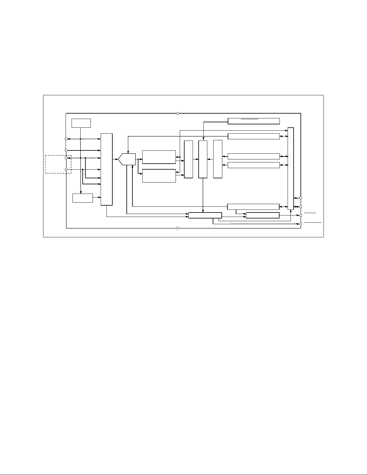
Figure 1.1 EMC1188 Block Diagram
SMSC EMC1188 7 Revision 1.0 (07-11-13)
DATASHEET
Page 8
EMC1188
10
9
8
7
6
SMDATA
SMCLK
1
2
3
4
5
ALERT
VDD
DP1
DN1
DN2 / DP3
DP2 / DN3 SYS_SHDN
GND
Exposed
pad
Quad Channel 1°C Temperature Sensor with Hardware Thermal Shutdown and 1.8V SMBus Communications
Datasheet
Chapter 2 Pin Description
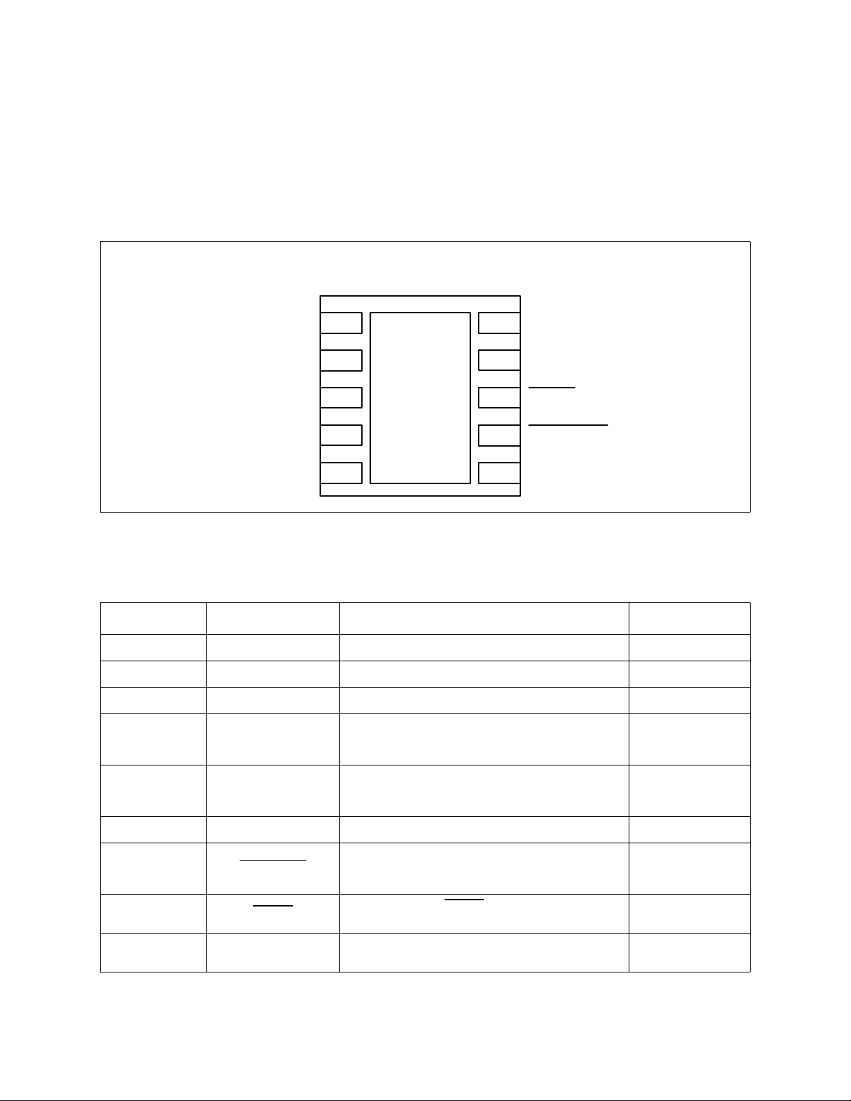
Figure 2.1 EMC1188 Pin Diagram DFN-10
Table 2.1 EMC1188 Pin Description
PIN NUMBER NAME FUNCTION TYPE
1 VDD Power supply Power
2 DP1 External diode 1 positive (anode) connection AIO
3 DN1 External diode 1 negative (cathode) connection AIO
4DP2 / DN3
5 DN2 / DP3
6 GND Ground Power
7 SYS_SHDN
8ALERT
9SMDATA
External diode 2 positive (anode) connection /
External Diode 3 negative (cathode) connection
for anti-parallel diodes
External diode 2 negative (cathode) connection /
External Diode 3 positive (anode) connection for
anti-parallel diodes
Active low system shutdown output signal requires pull-up resistor which selects the
Hardware Thermal Shutdown Limit
Active low digital ALERT output signal - requires
pull-up resist
SMBus Data input/output - requires pull-up
resistor
DIOD (5V)
AIO
AIO
OD (5V)
OD (5V)
Revision 1.0 (07-11-13) 8 SMSC EMC1188
DATASHEET
Page 9

Quad Channel 1°C Temperature Sensor with Hardware Thermal Shutdown and 1.8V SMBus Communications
T able 2.1 EMC1188 Pin Description (continued)
PIN NUMBER NAME FUNCTION TYPE
10 SMCLK SMBus Clock input - requires pull-up resistor DI (5V)
Datasheet
Bottom Pad Exposed Pad
Not internally connected, but recommend
grounding.
The pin types are described Table 2.2.
Ta ble 2.2 Pin Typ es
PIN TYPE DESCRIPTION
Power This pin is used to supply power or ground to the device.
AIO Analog Input / Output -This pin is used as an I/O for analog signals.
DI Digital Input - This pin is used as a digital input. This pin is 5V tolerant.
DIOD Digital Input / Open Drain Output - This pin is used as a digital I/O. When it is used as
an output, it is open drain and requires a pull-up resi stor. This pin is 5V tolerant.
OD Open Drain Digital Output - This pin is used as a digital output. It is open drain and
requires a pull-up resistor. This pin is 5V tolerant.
-
SMSC EMC1188 9 Revision 1.0 (07-11-13)
DATASHEET
Page 10
Quad Channel 1°C Temperature Sensor with Hardware Thermal Shutdown and 1.8V SMBus Communications
Datasheet
Chapter 3 Electrical Specifications
3.1 Absolute Maximum Ratings
Table 3.1 Abso lute Maximum Ratings
DESCRIPTION RATING UNIT
Supply Voltage (V
Voltage on 5V tolerant pins (V
Voltage on 5V tolerant pins (|V
Voltage on any other pin to Ground -0.3 to V
Operating Temperature Range -40 to +125 °C
Storage Temperature Range -55 to +150 °C
Lead Temperature Range Refer to JEDEC Spec. J-STD-020
ESD Rating, All pins HBM 2000 V
Note: Stresses at or above those listed could cause permanent damage to the device. This is a stress
Note 3.1 For the 5V tolerant pins that have a pull-up resistor (SMCLK, SMDATA,SYS_SHDN
) -0.3 to 4.0 V
DD
) -0.3 to 5.5 V
5VT_pin
- VDD|) (see Note 3.1)0 to 3.6 V
5VT_pin
+0.3 V
DD
rating only and functional operation of the device at any other conditio n above those indicated
in the operation sections of this specification is not implied.
ALERT), the pull-up voltage must not exceed 3.6V when the device is unpowered.
3.2 Electrical Specifications
Table 3.2 Electrical Specifications
and
V
= 3.0V to 3.6V, TA = -40°C to 125°C, all typical values at TA = 27°C unless otherwise noted.
DD
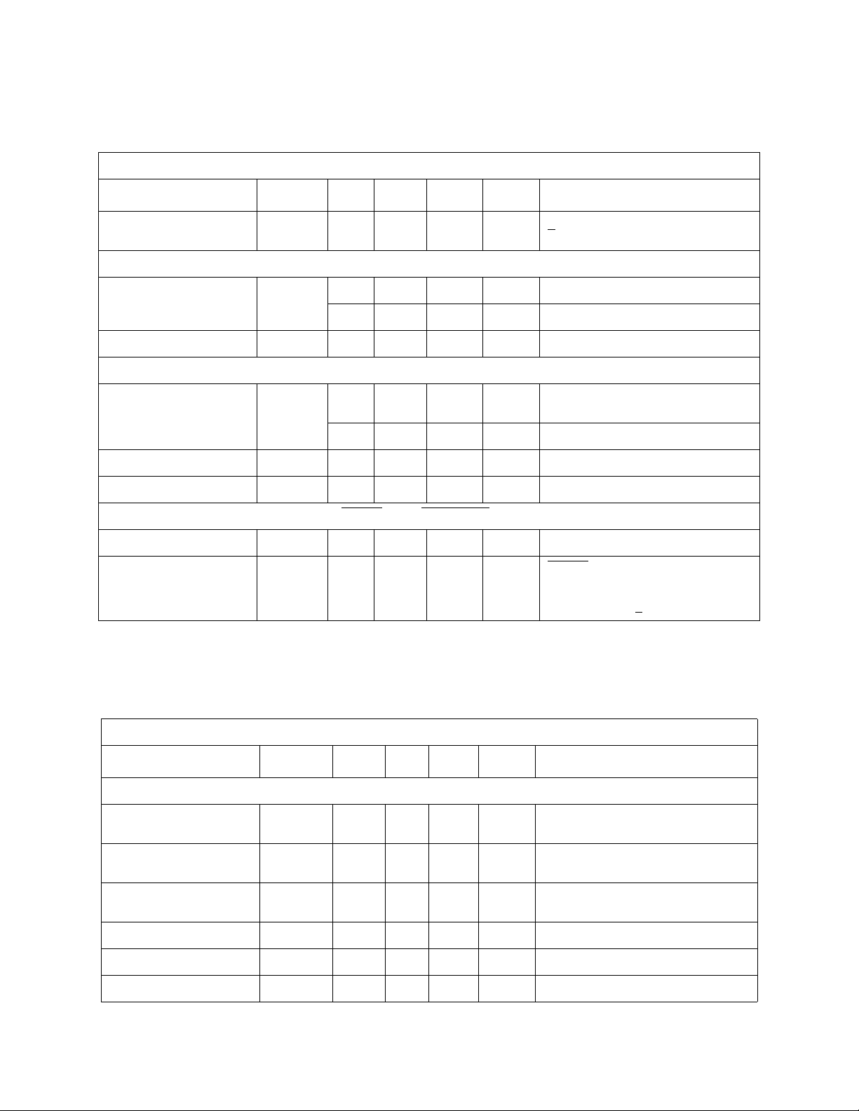
CHARACTERISTIC SYMBOL MIN T YP MAX UNITS CONDITIONS
DC Power
Supply Voltage V
Supply Current I
Revision 1.0 (07-11-13) 10 SMSC EMC1188
DD
DD
3.0 3.3 3.6 V
200 410 µA 0.0625 conversion / sec, dynamic
averaging disabled
215 425 µA 1 conversion / sec, dynamic
averaging disabled
325 465 µA 4 conversions / sec, dynamic
averaging disabled
890 1050 µA 4 conversions / sec, dynamic
averaging enabled
DATASHEET
Page 11
Quad Channel 1°C Temperature Sensor with Hardware Thermal Shutdown and 1.8V SMBus Communications
Table 3.2 Electrical Specifications (co ntinu ed)
V
= 3.0V to 3.6V, TA = -40°C to 125°C, all typical values at TA = 27°C unless otherwise noted.
DD
CHARACTERISTIC SYMBOL MIN TYP MAX UNITS CONDITIONS
Datasheet
1120 µA > 16 conversions / sec, dynamic
averaging enabled
Internal Temperature Monitor
Temperature Accuracy ±0.25 ±1 °C -5°C < TA < 100°C
±2 °C -40°C < T
< 125°C
A
Temperature Resolution 0.125 °C
External Temperature Monitor
Temperature Accuracy ±0.25 ±1 °C +20°C < T
0°C < TA < 100°C
±0.5 ±2 °C -40°C < T
DIODE
DIODE
< +110°C
< 127°C
Temperature Resolution 0.125 °C
Capacitive Filter C
Output Low Voltage V
Leakage Current I
FILTER
OL
LEAK
0.4 V I
2.2 2.7 nF Connected across external diode
ALERT
and SYS_SHDN pins
= 8mA
SINK
±5 µA ALERT and pins
Device powered or unpowered
TA < 85°C
pull-up voltage < 3.6V
3.3 SMBus Electrical Characteristics
Table 3.3 SMBus Electrical Specifications
V
= 3.0 to 3.6V, TA = -40°C to 125°C, all typical values are at TA = 27°C unless otherwise noted.
DD
CHARACTERISTIC SYMBOL MIN TYP MAX UNITS CONDITIONS
SMBus Interface
Input High Voltage V
Input Low Voltage V
Leakage Current I
IH
IL
LEAK
Hysteresis 50 mV
Input Capacitance C
Output Low Sink Current I
SMSC EMC1188 11 Revision 1.0 (07-11-13)
IN
OL
1.4 V
V 5V Tolerant. Voltage threshold
DD
based on 1.8V operation
-0.3 0.8 V 5V Tolerant. Voltage threshold
based on 1.8V operation
±5 µA Powered or unpowered
TA < 85°C
5pF
8.2 15 mA SMDATA = 0.4V
DATASHEET
Page 12

Quad Channel 1°C Temperature Sensor with Hardware Thermal Shutdown and 1.8V SMBus Communications
Datasheet
Tabl e 3.3 SMBus Electrical Specifications (continued)
V
= 3.0 to 3.6V, TA = -40°C to 125°C, all typical values are at TA = 27°C unless otherwise noted.
DD
CHARACTERISTIC SYMBOL MIN TYP MAX UNITS CONDITIONS
SMBus Timing
Clock Frequency f
Spike Suppression t
Bus Free Time Stop to
Start
Hold Time: Start t
Setup Time: Start t
Setup Time: Stop t
Data Hold Time t
Data Hold Time t
Data Setup Time t
Clock Low Period t
Clock High Period t
Clock/Data Fall time t
Clock/Data Rise time t
Capacitive Load C
Timeout t
SMB
SP
t
BUF
HD:STA
SU:STA
SU:STO
HD:DAT
HD:DAT
SU:DAT
LOW
HIGH
FALL
RISE
LOAD
TIMEOUT
10 400 kHz
50 ns
1.3 µs
0.6 µs
0.6 µs
0.6 µs
0 µs When transmitting to the master
0.3 µs When receiving from the master
100 ns
1.3 µs
0.6 µs
300 ns Min = 20+0.1C
300 ns Min = 20+0.1C
LOAD
LOAD
ns
ns
400 pF per bus line
25 35 ms Disabled by default
Revision 1.0 (07-11-13) 12 SMSC EMC1188
DATASHEET
Page 13
Quad Channel 1°C Temperature Sensor with Hardware Thermal Shutdown and 1.8V SMBus Communications
SMDATA
SMCLK
T
BUF
P
S
S - Start Condition
P - Stop Condition
PS
T
HIGH
T
LOW
T
HD:STA
T
SU:STO
T
HD:STA
T
HD:DAT
T
SU:DAT
T
SU:STA
T
FALL
T
RISE
Datasheet
Chapter 4 System Management Bus Interface Protocol
4.1 Communications Protocol
The EMC1188 communicates with a host controller, such as an SMSC SIO, through the SMBus. The
SMBus is a two-wire serial communication protocol between a computer host and its peripheral
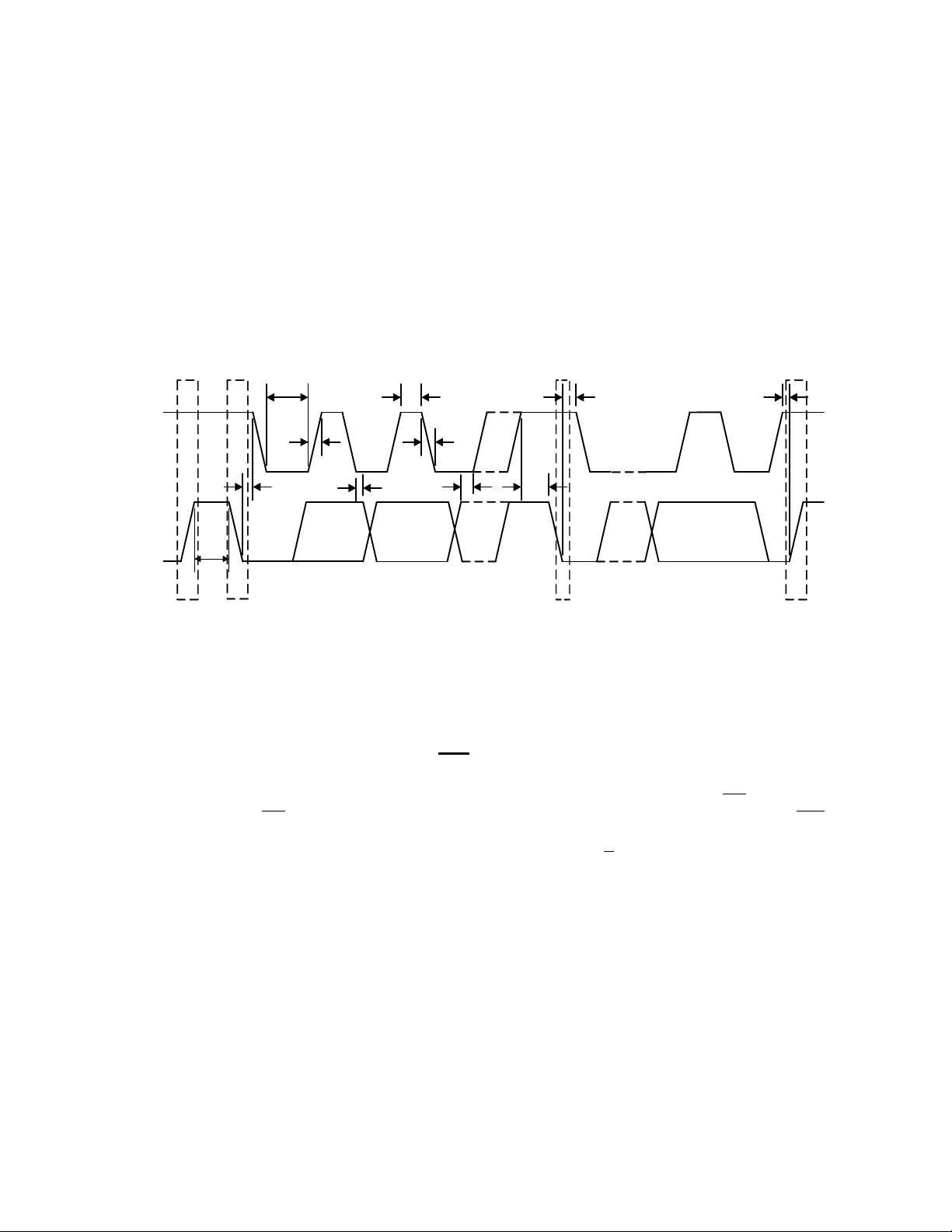
devices. A detailed timing diagram is shown in
For the first 15ms after power-up the device may not respond to SMBus communications.
.
Figure 4.1.
Figure 4.1 SMBus Timing Diagram
4.1.1 SMBu s Start Bit
The SMBus Start bit is defined as a transition of the SMBus Data line from a logic ‘1’ state to a logic
‘0’ state while the SMBus Clock line is in a logic ‘1’ state.
4.1.2 SMBus Add ress and RD / WR Bit
The SMBus Address Byte consists of the 7-bit client address followed by the RD / WR indicator bit. If
this RD / WR bit is a logic ‘0’, the SMBus Host is writing da ta to the client device. If this RD / WR bit
is a logic ‘1’, the SMBus Host is reading data from the client device.
The EMC1188-1 SMBus address is hard coded to 1001_1100(r/w).
4.1.3 SMBus Data Bytes
All SMBus Data bytes are sent most significant bit first and composed of 8-bits of information.
4.1.4 SMBus ACK and NACK Bits
SMSC EMC1188 13 Revision 1.0 (07-11-13)
The SMBus client will acknowledge all data bytes that it receives. This is done by the cl ient device
pulling the SMBus data line low after the 8th bit of each byte that is transmitted. This applies to the
Write Byte protocol.
The Host will NACK (not acknowledge) the last data byte to be received from the client by holding the
SMBus data line high after the 8th data bit has been sent.
DATASHEET
Page 14

Quad Channel 1°C Temperature Sensor with Hardware Thermal Shutdown and 1.8V SMBus Communications
Datasheet
4.1.5 SMBus Stop Bit
The SMBus Stop bit is defined as a transition of the SMBus Data line from a logic ‘0’ state to a logic
‘1’ state while the SMBus clock line is in a logic ‘1’ state. When the device detects an SMBus Stop bit
and it has been communicating with the SMBus protocol, it will rese t its client interface and prepare
to receive further communications.
4.1.6 SMBus Timeout
The EMC1188 supports SMBus Timeout. If the clock line is held low for longer than t
device will reset its SMBus protocol. This function can be enabled by setting the TIMEOUT bit (see
Section 6.13, "Consecutive ALERT Register 22h").
4.1.7 SMBus and I2C Compatibility
The EMC1188 is compatible with SMBus and I2C. The major differences between SMBus and I2C
devices are highlighted here. For more information, refer to the SMBus 2.0 and I2C specifications. For
information on using the EMC1188 in an I2C system, refer to SMSC AN 14.0 SMSC Dedicated Slave
Devices in I
1. EMC1188 supports I2C fast mode at 400kHz. This covers the SMBus max time of 100kHz.
2. Minimum frequency for SMBus communications is 10kHz.
3. The SMBus client protocol will reset if the clock is held at a logic ‘0’ for longer than 30ms. This
timeout functionality is disabled by default in the EMC1188 and can be enabled by writing to the
TIMEOUT bit. I2C does not have a timeout.
4. I2C devices do not support the Alert Response Address functionality (which is op tiona l for SMBus).
Attempting to communicate with the EMC1188 SMBus interface with an invalid slave address or invalid
protocol will result in no response from the device and will not affect its register contents. Stretching
of the SMCLK signal is supported, provided other devices on the SMBus control the timing.
2
C Systems.
4.2 SMBus Protocols
The device supports Send Byte, Read Byte, Write Byte, Receive Byte, and the Alert Response Address
as valid protocols as shown below.
All of the below protocols use the convention in Table 4.1.
TIMEOUT
, the
Ta ble 4.1 Protocol Format
DATA SENT
TO DEVICE
# of bits sent # of bits sent
Revision 1.0 (07-11-13) 14 SMSC EMC1188
DATASHEET
DATA SENT TO
THE HOST
Page 15

Quad Channel 1°C Temperature Sensor with Hardware Thermal Shutdown and 1.8V SMBus Communications
4.2.1 Write Byte
The Write Byte is used to write one byte of data to the registers, as shown in Table 4.2.
Datasheet
Table 4.2 Write Byte Protocol
START
SLAVE
ADDRESS WR
ACK
REGISTER
ADDRESS ACK
REGISTER
DATA ACK STOP
1 -> 0 YYYY_YYY 0 0 XXh 0 XXh 0 0 -> 1
4.2.2 Read Byte
The Read Byte protocol is used to read one byte of data from the registers as show n in Table 4.3.
Table 4.3 Read Byte Protocol
START SLAVE
ADDRESS
1 -> 0 YYYY_
YYY
WR ACK REGISTER
ADDRESS
ACK START SLAVE
ADDRESS
0 0 XXh 0 1 -> 0 YYYY_
YYY
RD ACK REGISTER
DATA
NACK STOP
10 XX 10 -> 1
4.2.3 Send Byte
The Send Byte protocol is used to set the internal address register pointer to the correct address
location. No data is transferred during the Send Byte protocol as shown in Table 4.4.
Table 4.4 Send Byte Protocol
REGISTER
ADDRESS ACK STOP
START
SLA VE
ADDRESS WR
ACK
1 -> 0 YYYY_YYY 0 0 XXh 0 0 -> 1
4.2.4 Receive Byte
The Receive Byte protocol is used to read data from a register when the internal register address
pointer is known to be at the right location (e.g. set via Send Byte). This is used for consecutive reads
of the same register as shown in
Table 4.5 Receive Byte Protocol
SLA VE
START
ADDRESS RD ACK REGISTER DATA NACK STOP
1 -> 0 YYYY_YYY 1 0 XXh 1 0 -> 1
SMSC EMC1188 15 Revision 1.0 (07-11-13)
Table 4.5.
DATASHEET
Page 16

Quad Channel 1°C Temperature Sensor with Hardware Thermal Shutdown and 1.8V SMBus Communications
Datasheet
4.3 Alert Response Address
The ALERT output can be used as a processor interrupt or as an SMBus Alert.
When it detects that the ALERT pin is asserted, the host will send the Alert Response Address (ARA)
to the general address of 0001_100xb. All devices with active interrupts will respond with their client
address as shown in
ALERT
RESPONSE
START
ADDRESS RD
1 -> 0 0001_100 1 0 YYYY_YYY 1 0 -> 1
The EMC1188 will respond to the ARA in the following way:
1. Send Slave Address and verify that full slave address was sent (i.e. the SMBus communication
from the device was not prematurely stopped due to a bus contention event).
2. Set the MASK_ALL bit to clear the ALERT pin.
Table 4.6.
Ta ble 4.6 Alert Respo nse Address Protocol
DEVICE
ACK
ADDRESS NACK STOP
APPLICATION NOTE: The ARA does not clear the Status Register and if the MASK_ALL bit is cleared prior to the
Status Register being cleared, the ALERT
pin will be reasserted.
Revision 1.0 (07-11-13) 16 SMSC EMC1188
DATASHEET
Page 17
Quad Channel 1°C Temperature Sensor with Hardware Thermal Shutdown and 1.8V SMBus Communications
CPU
EMC1188
DP1
DN1
Thermal
diode
Internal
Diode
DN2 / DP3
DP2 / DN3
Optional
Anti-parallel
diode
Host
SMDATA
SMCLK
SMBus
Interface
SYS_SHDN
ALERT
Power
Control
1.8V – 3.3V
VDD
VDD = 3.3V
Chapter 5 Product Description
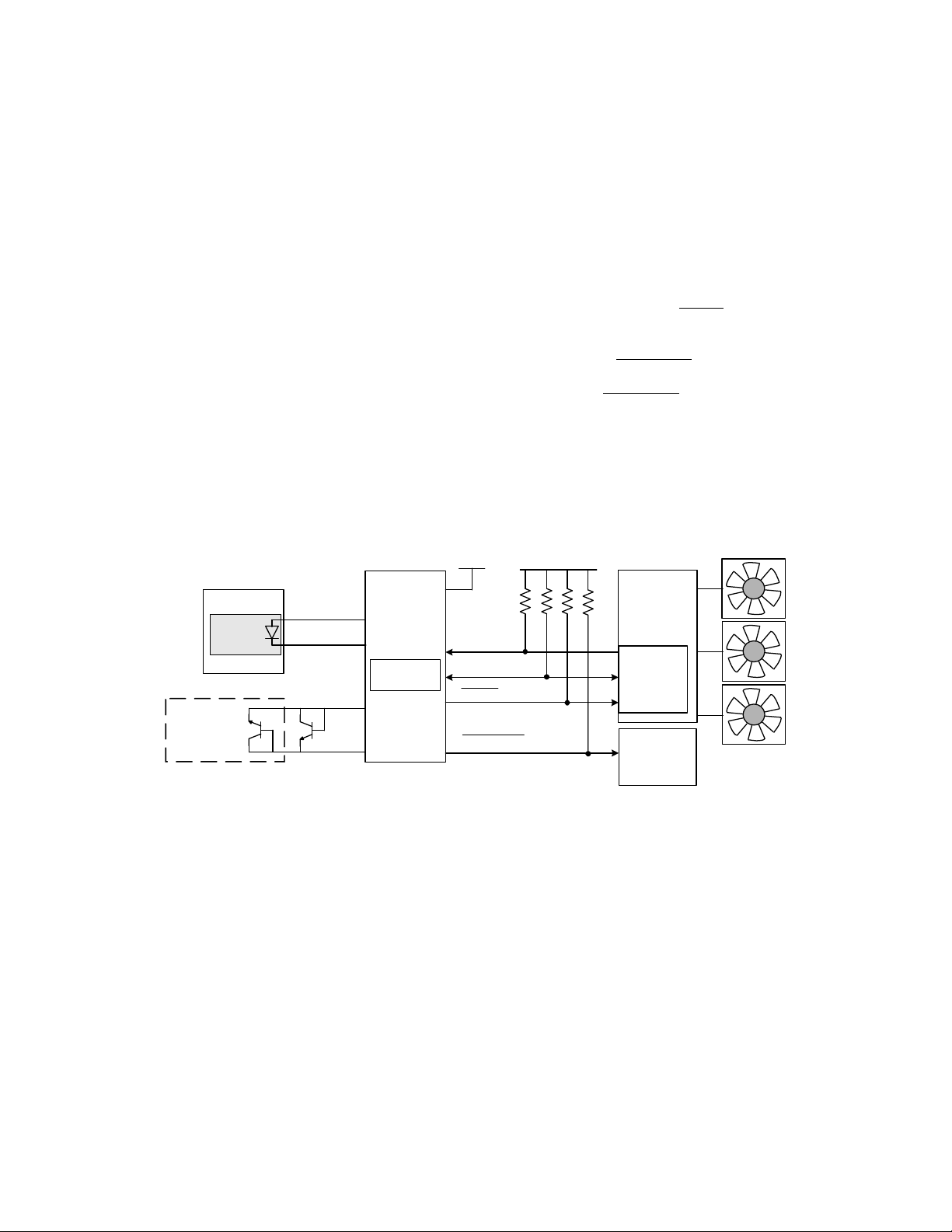
The is an SMBus temperature sensor with Hardware Thermal Shutdown. The EMC1188 monitors one
internal diode and up to three externally connected temperature diodes.
Thermal management is performed in cooperation with a host device. This consists of the host reading
the temperature data of both the external and internal temperature diodes of the EMC 1188 and using
that data to control the speed of one or more fans.
The EMC1188 has two levels of monitoring. The first provides a maskable ALERT signal to the host
when the measured temperatures exceeds user programmable limits. This allows the EMC1188 to be
used as an independent thermal watchdog to warn the host of temperature hot spots without direct
control by the host. The second level of monitoring asserts the
Diode temperature exceeds a hardware specified threshold temperature.Additionall y, the internal diode
and External Diode 2 and 3 can be configured to assert the
temperature exceeds user programmable limits.
For the EMC11 88, External Diode channels 2 and 3 are only compatible with general purpose diodes
(such as a 2N3904).
Figure 5.1 shows a system level block diagram of the EMC1188.
Datasheet
SYS_SHDN pin when the External
SYS_SHDN pin when the measured
Figure 5.1 System Diagram for EMC1188
5.1 Conversion Rates
The EMC1188 may be configured for different conversion rates based on the system requirements.
The conversion rate is configured as described in
Section 6.5. The default conversion rate is 4
conversions per second. Other available conversion rates are shown in Table 6.6, "Conversion Rate".
5.2 Dynamic Averaging
Dynamic averaging causes the EMC1188 to measure the external diode channels for an extended time
based on the selected conversion rate. This functionality can be disabled for increased power savings
at the lower conversion rates (see
averaging is enabled, the device will automatically adjust the samp ling and measurement time for the
external diode channels. This allows the device to average 2x or 16x longer tha n the normal 11 bit
operation (nominally 21ms per channel) while still maintaining the selected conversion rate. The
SMSC EMC1188 17 Revision 1.0 (07-11-13)
Section 6.4, "Configuration Register 03h / 09h"). When dynamic
DATASHEET
Page 18

Quad Channel 1°C Temperature Sensor with Hardware Thermal Shutdown and 1.8V SMBus Communications
Datasheet
benefits of dynamic averaging are improved noise rejection due to the longer integrat ion time as well
as less random variation of the temperature measure ment.
When enabled, the dynamic averaging applies when a one-sh ot command is issued. The device will
perform the desired averaging during the one-shot operation according to the selected conversion rate.
When enabled, the dynamic averaging will affect the average supply current based on the chosen
conversion rate as shown in
Table 5.1.
Ta ble 5.1 Supply Current vs. Conversion Rate for EMC1188
CONVERSION RATE
AVERAGE SUPPLY CURRENT
(TYPICAL)
ENABLED
(DEFAULT) DISABLED
AVERAGING FACTOR (BASED ON
11-BIT OPERATION)
ENABLED
(DEFAULT) DISABLED
1 / 16 sec 230uA 220uA 16x 1x
1 / 8 sec 275uA 220uA 16x 1x
1 / 4 sec 350uA 220uA 16x 1x
1 / 2 sec 405uA 220uA 16x 1x
1 / sec 480uA 250uA 8x 1x
2 / sec 850uA 290uA 4x 1x
4 / sec (default) 890uA 370uA 2x 1x
8 / sec 970uA 525uA 1x 1x
16 / sec 990uA 690uA 0.5x 0.5x
32 / sec 1030uA 1050uA 0.25x 0.25x
64 / sec 1500uA 1100uA 0.125x 0.125x
5.3 .SYS_SHDN Output
The SYS_SHDN output is asserted independently of the ALERT output and cannot be masked. If the
External Diode 1 temperature exceeds the Hardware Thermal Shutdown Limit for the programmed
number of consecutive measurements, the
The Hardware Thermal Shutdown Limit is defined at power-up via the pull-up resistors on the
SYS_SHDN and ALERT pins as shown in Table 5.2. This limit cannot be modified or masked via
software.
In addition to External Diode 1 channel triggering the SYS_SHDN pin when the measured temperat ure
exceeds to the Hardware Thermal Shutdown Limit, each of the measurement channels can be
configured to assert the
SYS_SHDN pin when they exceed the corresponding THERM Limit.
When the SYS_SHDN pin is asserted, it will not release until the External Diode 1 temperature drops
below the Hardware Thermal Shutdown Limit minus 10°C and all other measured temperature s drop
below the THERM Limit minus the THERM Hysteresis value (when linked to
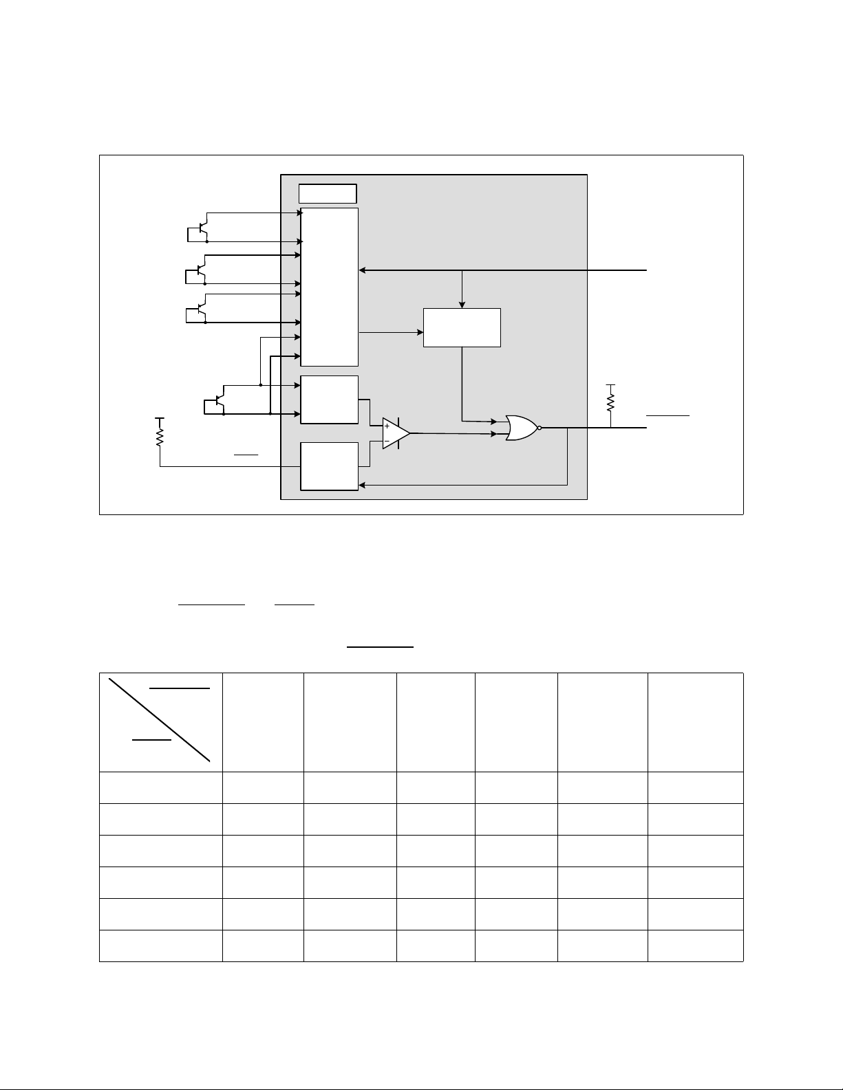
Figure 5.2 shows a block diagram of the interaction between the input channe ls and the SYS_SHDN
pin.
Revision 1.0 (07-11-13) 18 SMSC EMC1188
SYS_SHDN pin is asserted.
SYS_SHDN).
DATASHEET
Page 19
Quad Channel 1°C Temperature Sensor with Hardware Thermal Shutdown and 1.8V SMBus Communications
Temperature
Conversion
Function
Select
HW_SHDN
H/W Thermal
Shutdown Sensor
Hardware Thermal Shutdown
S/W Set Sensor
SMBus
Traffic
SW_SHDN
3.3V
ALERT
S/W Set Sensor
SYS_SHDN
Temperature
Conversion
and up to 4
THERM Limit
Registers
Software
Shutdown Enable
3.3V
Internal Diode
S/W Set Sensor
(EMC1188 only)
SYS_SHD
PULL-UP
PULL-UP
ALERT
Datasheet
Figure 5.2 Block Diagram of Hardware Thermal Shutdown
5.4 Hardware Thermal Shutdown Limit
The Hardware Thermal Shutdown Limit temperature is determined by pull-up resistors on the
SYS_SHDN and ALERT pins shown in Table 5.2.
Threshold Temperature
10K OHM
±10%
4.7K OHM ±10%
6.8K OHM ±10%
10K OHM ±10%
15K OHM ±10%
22K OHM ±10%
Table 5.2 SYS_SHDN
4.7K OHM
±10%
6.8K OHM
±10%
77°C 83°C 89°C 95°C 101°C 107°C
78°C 84°C 90°C 96°C 102°C 108°C
79°C 85°C 91°C 97°C 103°C 109°C
80°C 86°C 92°C 98°C 104°C 110°C
81°C 87°C 93°C 99°C 105°C 111°C
15K OHM
±10%
22K OHM
±10%
33K OHM
±10%
33K OHM ±10%
SMSC EMC1188 19 Revision 1.0 (07-11-13)
82°C 88°C 94°C 100°C 106°C 112°C
DATASHEET
Page 20

Quad Channel 1°C Temperature Sensor with Hardware Thermal Shutdown and 1.8V SMBus Communications
Datasheet
5.5 ALERT Output
The ALERT pin is an open drain output and requi res a pull-up resistor to VDD and has two modes of
operation: interrupt mode and comparator mode. The mo de of the
ALERT / COMP bit in the Configuration Register (see
5.5.1 ALERT Pin Interrupt Mode
When configured to operate in interrupt mode, the ALERT pin asserts low when an out of limit
measurement (
functioning as any standard
as an out-of-limit condition remains. Once th e out-of-limit con dition has been remo ved, the
will remain asserted until the appropriate status bits are cleared.
The ALERT pin can be masked by setting the MASK_ALL bit. Once the ALERT pin has been masked,
it will be de-asserted and remain de-asserted until the MASK_ALL bit is cleared by the user. Any
interrupt conditions that occur while the
There are also individual channel masks (see
The ALERT pin is used as an interrupt signal or as an SMBus Alert signal tha t allows an SMBus slave
to communicate an error condition to the master. One or more
together.
> high limit or < low limit) is dete cted on any diode or when a diode fault i s detected,
ALERT in on the SMBus. The ALERT pin will remain asserted as long
Section 6.4).
ALERT pin is masked will update the Status Regist er normally.
Section 6.12).
ALERT output is selected via the
ALERT outputs can be hard-wired
ALERT pin
5.5.2 ALERT Pin Comparator Mode
When the ALERT pin is configured to operate in comparator mode, it will be asserted if any of the
measured temperatures exceeds the respective high limit. The
all temperatures drop below the corresponding high l imit minus the Therm Hysteresis value.
When the ALERT pin is asserted in comparator mode, the corresponding high limit status bits will be
set. Reading these bits will not clear them until the
deasserted, the status bits will be automatically cleared.
The MASK_ALL bit will not block the ALERT pin in this mode; however, the individual channel masks
Section 6.12) will prevent the respective channel from asserting t he ALERT pin.
(see
ALERT pin is deasserted. Once the ALERT pin is
ALERT pin will remain asserted until
5.6 ALERT and SYS_SHDN Pin Considerations
Because of the decode method used to determine the Hardware Thermal Shutdown Limit, it is
important that the pull-up resistance on both the
shown in
connected to the same 3.3V supply that drives the VDD pin.
For 15ms after power up, the ALERT and SYS_SHDN pins must not be pulled low or the Hardware
Thermal Shutdown Limit will not be decoded properly. If the system requirements do not permit these
conditions, the
time.
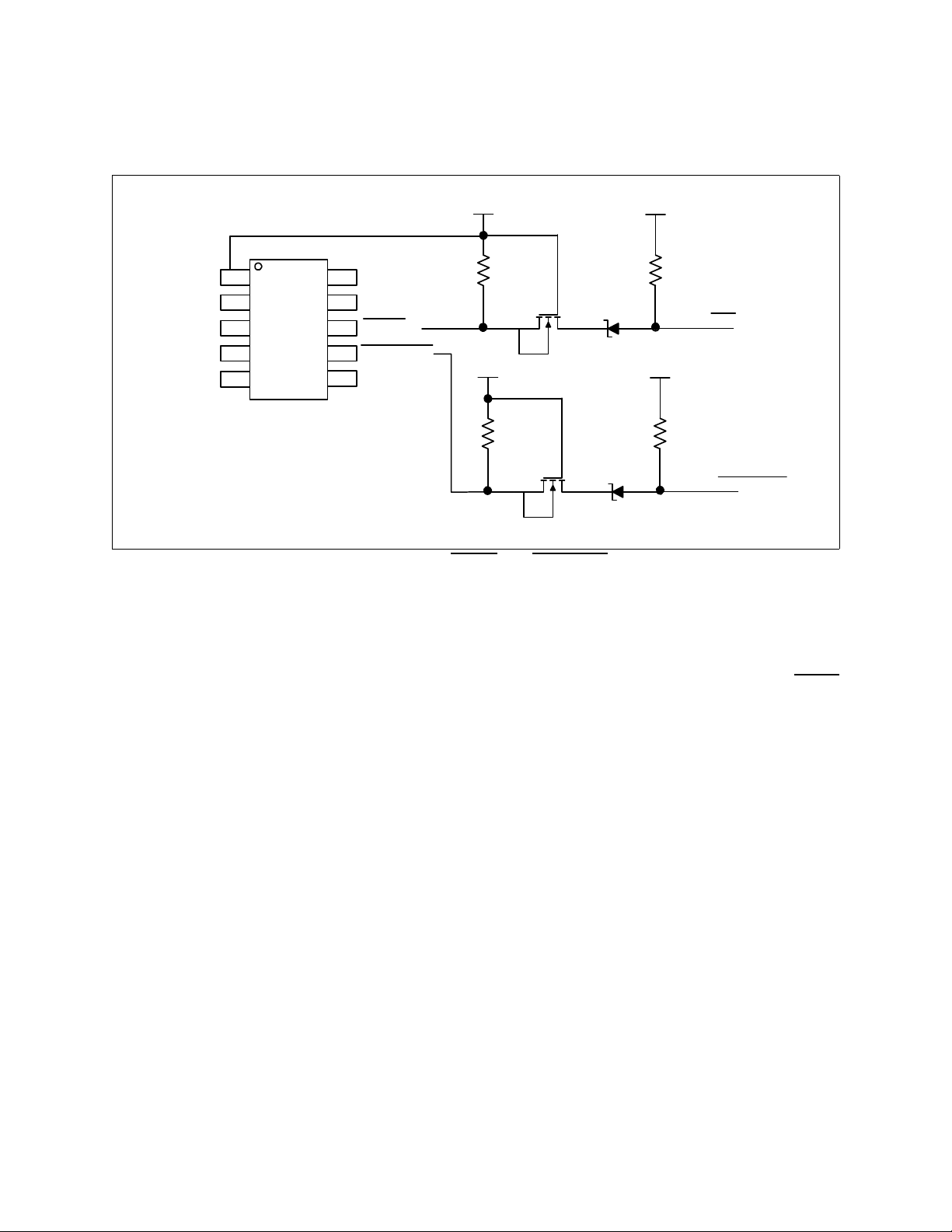
One method of isolating the ALERT pin is shown in Figure 5.3.
Table 5.2. Additionally, the pull-up resistor on the ALERT and SYS_SHDN pins must be
ALERT and SYS_SHDN pins must be isolated from their respective busses during this
ALERT and SYS_SHDN pins be within the tolerances
Revision 1.0 (07-11-13) 20 SMSC EMC1188
DATASHEET
Page 21
Quad Channel 1°C Temperature Sensor with Hardware Thermal Shutdown and 1.8V SMBus Communications
EMC1188
10
9
8
7
SMDATA
SMCLK
1
2
3
4
ALERT
VDD
DP1
DN1
SYS_SHDN
GND
+3.3V
22K
4.7K 33K
+2.5 - 5V
5 6
DP2/DN3
DN2/DP3
+3.3V
22K
4.7K -
33K
+2.5 - 5V
Shared SYS_SHDN
Shared Alert
Datasheet
Figure 5.3 Isolating ALERT and SYS_SHDN Pin
5.7 Temperature Measurement
The EMC1188 can monitor the temperature of up to three externally connected diode.
The device contains programmable High, Low, and Therm limits for all measured temperature
channels. If the measured temperature goes below the Low limit or above the High limit, the
pin can be asserted (based on user settings).
5.7.1 Beta Compensation
The EMC1188 is configured to monitor the temperature of basic diodes (e.g., 2N3904) or CPU thermal
diodes. It automatically detects the type of exte rnal diode (CPU diode or diode connected transistor)
and determines the optimal setting to reduce temperature errors introduced by beta variation.
Compensating for this error is also known as implementing the transistor or BJT model for temperature
measurement.
For discrete transistors configured with the collector and b ase shorted together, the beta is generally
sufficiently high such that the percent change in beta variation is very small. For example, a 10%
variation in beta for two forced emitter currents with a transistor whose id eal beta is 50 would contribute
approximately 0.25°C error at 100°C. However for substrate transistors where the base-emitte r juncti on
is used for temperature measurement and the collector is tied to the substrate, the proportional beta
variation will cause large error. For example, a 10% variation in beta for two forced emitter currents
with a transistor whose ideal beta is 0.5 would contribute approximately 8.25°C error at 100°C.
5.7.2 Resistance Error Correction (REC)
For the EMC1188 the External Diode 2 and External Diode 3 channels do not support Beta
Compensation.
Parasitic resistance in series with the external diodes will limit the accuracy obtainable from
temperature measurement devices. The voltage developed across this resistance by the switching
diode currents cause the temperature measurement to read higher than the true temperature.
SMSC EMC1188 21 Revision 1.0 (07-11-13)
ALERT
DATASHEET
Page 22

Quad Channel 1°C Temperature Sensor with Hardware Thermal Shutdown and 1.8V SMBus Communications
Datasheet
Contributors to series resistance are PCB trace resistance, on die (i.e. on the processor) metal
resistance, bulk resistance in the base and emitter of the temperat ure transistor. Typically, the error
caused by series resistance is +0.7°C per ohm. The EMC1188 automat ically corrects up to 100 ohms
of series resistance.
5.7.3 Programmable External Diode Ideality Factor
The EMC1188 is designed for external diodes with an ideality factor of 1.008. Not all external diodes,
processor or discrete, will have this exact value. This variation of the ideality factor introduces error in
the temperature measurement which must be corrected for. This correction is typically done using
programmable offset registers. Since an ideality factor mismatch introduces an error that is a function
of temperature, this correction is only accurate within a small range of temperatures. To provide
maximum flexibility to the user, the EMC1188 provides a 6-bit reg ister for each external diode where
the ideality factor of the diode used is programmed to eliminate errors across all temperatures.
APPLICATION NOTE: When monitoring a substrate transistor or CPU diode and b eta compensation is ena bled, the
Ideality Factor should not be adjusted. Beta Compensation automatically corrects for most
ideality errors.
5.8 Diode Faults
The EMC1188 detects an open on the DP and DN pins, and a short across the DP and DN pins. For
each temperature measurement made, the device checks for a diode fault on the external diode
channel(s). When a diode fault is detect ed, the
and the temperature data reads 00h in the MSB and LSB registers (note: the low limit will not be
checked). A diode fault is defined as one of the following: an open be tween DP and DN, a short from
to DP, or a short from VDD to DN.
V
DD
If a short occurs across DP and DN or a short occurs from DP to GND, the low limit status bit is set
and the
measurement of 0.000°C (-64°C in extended range) resulting in temperature data of 00h in the MSB
and LSB registers.
If a short from DN to GND occurs (with a diode connected), temperature measurements will continue
as normal with no alerts.
ALERT pin asserts (unless masked). This condition is indistinguishabl e from a temperature
5.9 Consecutive Alerts
The EMC1188 contain multiple consecutive alert counters. One set of counters applies to the ALERT
pin and the second set of counters applies to the SYS_SHDN pin. Each temperature measurement
channel has a separate consecutive alert counter for each of the
counters are user programmable and determine the number of consecutive measurements that a
temperature channel(s) must be out-of-limit or reporting a diode fault before t he corresponding pin is
asserted.
See Section 6.13, "Consecutive ALERT Register 22h" for more details on the consecutive alert
function.
5.10 Digital Filter
ALERT pin asserts (unless masked, see Section 5.9)
ALERT and SYS_SHDN pins. All
To reduce the effect of noise a nd temperature spikes on the report ed temperature, the External Diode
channel uses a programmable digital filter. This filter can be configured as Level 1, Level 2, or Disabled
(default) (see
Revision 1.0 (07-11-13) 22 SMSC EMC1188
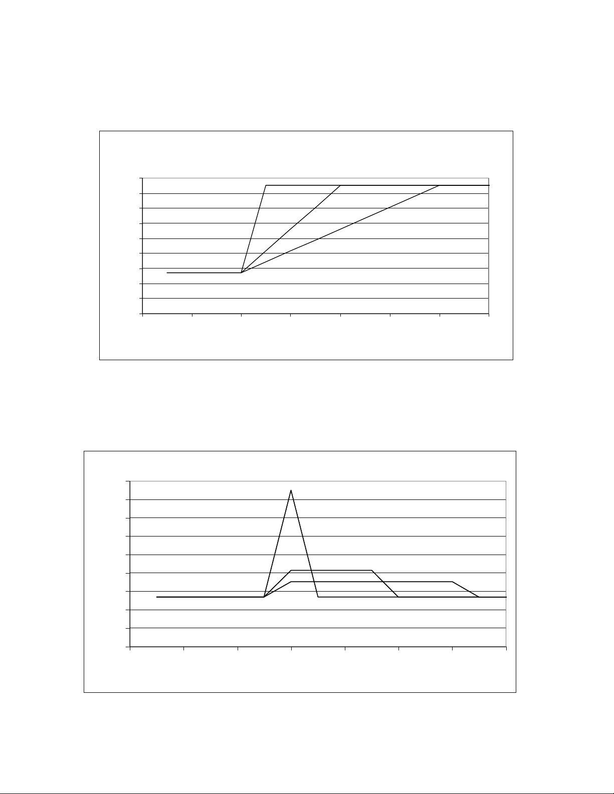
Section 6.19). The typical filter performance is sh own in Figure 5.4 and Figure 5.5.
DATASHEET
Page 23
Quad Channel 1°C Temperature Sensor with Hardware Thermal Shutdown and 1.8V SMBus Communications
Filter Step Response
0
10
20
30
40
50
60
70
80
90
02468101214
Samples
Temperature (C)
Disabled
Level1
Level2
Filter Impulse Response
0
10
20
30
40
50
60
70
80
90
02468101214
Samples
Temperatu r e (C)
Disabled
Level1
Level2
Datasheet
Figure 5.4 Temperature Filter Step Response
SMSC EMC1188 23 Revision 1.0 (07-11-13)
Figure 5.5 Temperature Filter Impulse R esponse
DATASHEET
Page 24

Quad Channel 1°C Temperature Sensor with Hardware Thermal Shutdown and 1.8V SMBus Communications
Datasheet
5.11 Temperature Measurement Results and Data
The temperature measurement results are stored in the internal and extern al temperature registers.
These are then compared with the values stored in the high and low limit registers. Both externa l and
internal temperature measurements are stored in 11-bit format with the eight (8) most significant bits
stored in a high byte register and the three (3) least significant bits stored in the three (3) MSB
positions of the low byte register. All other bits of the low byte register are set to zero.
The EMC1188 has two selectable temperature ranges. The default range is from 0°C to +127°C a nd
the temperature is represented as binary number able to report a temperature f rom 0°C to +127 .875°C
in 0.125°C steps.
The extended range is an extended temper ature range from -64°C to +191°C. The data format is a
binary number offset by 64°C. The extended range is used to measure temperature diodes w ith a large
known offset (such as AMD processor diodes) where the diode temperature plus the offset would be
equivalent to a temperature higher than +127°C.
Table 5.3 shows the default and extende d range formats.
Table 5.3 Temperature Data Format
TEMPERATURE (°C) DEFAULT RANGE 0°C TO 127°C EXTENDED RANGE -64°C TO 191°C
Diode Fault 000 0000 0000 000 0000 0000
-64 000 0000 0000 000 0000 0000
- 1 0 00 0 0 0 0 0 0 0 0 0 0 1 1111 1 0 0 0
0 000 0000 0000 010 0000 0000
0.125 000 0000 0001 010 0000 0001
1 000 0000 1000 010 0000 1000
64 010 0000 0000 100 0000 0000
65 010 0000 1000 100 0000 1000
12 7 011 1111 1 0 0 0 10 1 1111 1 0 0 0
12 7 . 8 7 5 011 1111 1111 10 1 1111 1111
128 011 1111 1111 110 0000 0000
19 0 011 1111 1111 111 1111 0000
19 1 011 1111 1111 111 1111 1000
>= 1 9 1 . 8 7 5 0 11 1111 1111 111 1111 1111
Revision 1.0 (07-11-13) 24 SMSC EMC1188
DATASHEET
Page 25

Quad Channel 1°C Temperature Sensor with Hardware Thermal Shutdown and 1.8V SMBus Communications
Chapter 6 Register Description
The registers shown in Table 6.1 are accessible through the SMBus. An entry of ‘-’ indicates that the
bit is not used and will always read ‘0’.
Table 6.1 Register Set in Hexadecimal Order
Datasheet
REGISTER
ADDRESS R/W REGISTER NAME FUNCTION
00h R
01h R
02h R Status
03h R/W Configuration
04h R/W Conversion Rate
05h R/W
06h R/W
07h R/W
Internal Diode Data
High Byte
External Diode Data
High Byte
Internal Diode High
Limit
Internal Diode Low
Limit
External Diode High
Limit High Byte
Stores the integer data for the
Internal Diode
Stores the integer data for External
Diode
Stores the status bits for the
Internal Diode and External Diode
Controls the general operation of
the device (mirrored at address
09h)
Controls the conversion rate for
updating temperature data
(mirrored at address 0Ah)
Stores the 8-bit high limit for the
Internal Diode (mirrored at address
0Bh)
Stores the 8-bit low limit for the
Internal Diode (mirrored at address
0Ch)
Stores the integer portion of the
high limit for External Diode
(mirrored at register 0Dh)
DEFAULT
VALUE PAGE
00h
Page 28
00h
00h Page 28
Page 30
06h
(4/sec)
55h
(85°C)
00h
(0°C)
55h
(85°C)
Page 31
Page 32
08h R/W
09h R/W Configuration
0Ah R/W Conversion Rate
SMSC EMC1188 25 Revision 1.0 (07-11-13)
External Diode Low
Limit High Byte
Stores the integer portion of the
low limit for External Diode
(mirrored at register 0Eh)
Controls the general operation of
the device (mirrored at address
03h)
Controls the conversion rate for
updating temperature data
(mirrored at address 04h)
DATASHEET
00h
(0°C)
06h
(4/sec)
Page 30
Page 31
Page 26

Quad Channel 1°C Temperature Sensor with Hardware Thermal Shutdown and 1.8V SMBus Communications
Datasheet
Table 6.1 Register Set in Hexadecimal Order (continued)
REGISTER
ADDRESS R/W REGISTER NAME FUNCTION
0Bh R/W
0Ch R/W
0Dh R/W
0Eh R/W
10h R
Internal Diode High
Limit
Internal Diode Low
Limit
External Diode High
Limit High Byte
External Diode Low
Limit High Byte
External Diode Data
Low Byte
11h R/W Scratchpad
12h R/W Scratchpad
13h R/W
14h R/W
External Diode High
Limit Low Byte
External Diode Low
Limit Low Byte
Stores the 8-bit high limit for the
Internal Diode (mirrored at address
05h)
Stores the 8-bit low limit for the
Internal Diode (mirrored at address
06h)
Stores the integer portion of the
high limit for External Diode
(mirrored at register 07h)
Stores the integer portion of the
low limit for External Diode
(mirrored at register 08h)
Stores the fractional data for
External Diode
Scratchpad register for software
compatibility
Scratchpad register for software
compatibility
Stores the fractional portion of the
high limit for External Diode
Stores the fractional portion of the
low limit for External Diode
DEFAULT
VALUE PAGE
55h
(85°C)
00h
(0°C)
Page 32
55h
(85°C)
00h
(0°C)
00h Page 28
00h Page 33
00h Page 33
00h
Page 32
00h
15h R/W
External Diode 2
High Limit High Byte
Stores the integer portion of the
high limit for External Diode 2
55h
(85°C)
Page 32
16h R/W
17h R/W
External DIode 2 Low
Limit High Byte
External Diode 2
High Limit Low Byte
Stores the integer portion of the
low limit for External Diode 2
Stores the fractional portion of the
high limit External Diode 2
00h
(0°C)
00h
Page 32
18h R/W
19h R/W
1Ah R/W
External Diode 2 Low
Limit Low Byte
External Diode
Therm Limit
External Diode 2
Therm Limit
Stores the fractional portion of the
low limit for External Diode 2
Stores the 8-bit critical temperature
limit for External Diode
Stores the 8-bit critical temperature
limit for External Diode 2
00h
55h
(85°C)
55h
(85°C)
Page 33
Page 33
Stores status bits indicating which
1Bh R-C Extern al Diode Fault
external diode detected a diode
00h Page 34
fault
1Dh R/W
Revision 1.0 (07-11-13) 26 SMSC EMC1188
SYS_SHDN
Configuration
Controls which software channels,
if any, are linked to the
SYS_SHDN
pin
00h Page 34
DATASHEET
Page 27

Quad Channel 1°C Temperature Sensor with Hardware Thermal Shutdown and 1.8V SMBus Communications
Datasheet
Table 6.1 Register Set in Hexadecimal Order (continued)
REGISTER
ADDRESS R/W REGISTER NAME FUNCTION
1Eh R
1Fh R/W
20h R/W
Hardware Thermal
Shutdown Limit
Channel Mask
Register
Internal Diode Therm
Limit
21h R/W Therm Hysteresis
When read, returns the selected
Hardware Thermal Shutdown Limit
Controls the masking of individual
channels
Stores the 8-bit critical temperature
limit for the Internal Diode
Stores the 8-bit hysteresis value
that applies to all Therm limits
Controls the number of out-of-limit
22h R/W Consecutive ALERT
conditions that must occur before
an interrupt is asserted
23h R
24h R
26h R/W
27h R/W
External Diode 2
Data High Byte
External Diode 2
Data Low Byte
External Diode 2
Beta Configuration
External Diode
Ideality Factor
Stores the integer data for External
Diode 2
Stores the fractional data for
External Diode 2
Stores the Beta Compensation
circuitry settings for External Diode
2
Stores the ideality factor for
External Diode
DEFAULT
VALUE PAGE
N/A Page 35
00h Page 36
55h
(85°C
Page 33
0Ah
(10°C)
70h Page 36
00h
Page 28
00h
08h
07h
Page 39
(EMC1188)
12h
(1.008)
Page 39
28h R/W
29h R
2Ah R
2Bh R
2Ch R/W
2Dh R/W
2Eh R/W
2Fh R/W
30h R/W
31h R/W
External Diode 2
Ideality Factor
Internal Diode Data
Low Byte
External Diode 3
High Byte
External Diode 3 Low
Byte
External Diode 3
High Limit High Byte
External Diode 3 Low
Limit High Byte
External Diode 3
High Limit Low Byte
External Diode 3 Low
Limit Low Byte
External Diode 3
Therm Limit
External Diode 3
Ideality Factor
Stores the ideality factor for
External Diode 2
Stores the fractional data for the
Internal Diode
Stores the integer data for External
Diode 3
Stores the fractional data for
External Diode 3
Stores the integer portion of the
high limit for External Diode 3
Stores the integer portion of the
low limit for External Diode 3
Stores the fractional portion of the
high limit for External Diode 3
Stores the fractional portion of the
low limit for External Diode 3
Stores the 8-bit critical temperature
limit for External Diode 3
Stores the ideality factor for
External Diode 3
12h
(1.008)
Page 39
00h Page 28
00h
Page 28
00h
55h
(85°C)
00h
(0°C)
Page 32
00h
00h
55h
(85°C)
12h
(1.008)
Page 33
Page 39
SMSC EMC1188 27 Revision 1.0 (07-11-13)
DATASHEET
Page 28

Quad Channel 1°C Temperature Sensor with Hardware Thermal Shutdown and 1.8V SMBus Communications
Datasheet
Table 6.1 Register Set in Hexadecimal Order (continued)
REGISTER
ADDRESS R/W REGISTER NAME FUNCTION
35h R-C High Limit Status Status bits for the High Limits 00h Page 41
36h R-C Low Limit Status Status bits fo r the Low Limits 00h Page 41
37h R Therm Limit Status Status bits for the Therm Limits 00h Page 42
40h R/W Filter Control
FDh R
FEh R Ma nufacturer ID
FFh R Revision
Product ID
(EMC1824)
Controls the digital filter setting for
the External Diode channel
Stores a fixed value that identifies
the device
Stores a fixed value that
represents SMSC
Stores a fixed value that
represents the revision number
DEFAULT
VALUE PAGE
00h Page 42
27h Page 43
5Dh Page 43
07h Page 43
6.1 Data Read Interlock
When any temperature channel high byte register is read, the corresponding low byte is copied into
an internal ‘shadow’ register. The user is free to read the low byte at any time and be guarantee d that
it will correspond to the previously read high byte. Regardless if the low byte is read or not, readi ng
from the same high byte register again will automa tically refresh this stored low byte data.
6.2 Temperature Data Registers
T able 6.2 Temperature Data Registers
ADDR R/W REGISTER B7 B6 B5 B4 B3 B2 B1 B0 DEFAULT
00h R
29h R
01h R
10h R
23h R
24h R
Internal Diode
High Byte
Internal Diode
Low Byte
External Diode
High Byte
External Diode
Low Byte
External Diode
2 High Byte
External Diode
2 Low Byte
128 64 32 16 8 4 2 1 00h
0.5 0.25 0.125 - - - - - 00h
128 64 32 16 8 4 2 1 00h
0.5 0.25 0.125 - - - - - 00h
128 64 32 16 8 4 2 1 00h
0.5 0.25 0.125 - - - - - 00h
Revision 1.0 (07-11-13) 28 SMSC EMC1188
DATASHEET
Page 29

Quad Channel 1°C Temperature Sensor with Hardware Thermal Shutdown and 1.8V SMBus Communications
Datasheet
Table 6.2 Temperature Data Registers (continued)
ADDR R/W REGISTER B7 B6 B5 B4 B3 B2 B1 B0 DEFAULT
2Ah R
2Bh R
As shown in Table 6.2, all temperatures are stored as an 11-bit value with the high byte representing
the integer value and the low byte representing th e fractional value left justified to occupy t he MSBits.
External Diode
3 High Byte
External Diode
3 Low Byte
128 64 32 16 8 4 2 1 00h
0.5 0.25 0.125 - - - - - 00h
6.3 Status Register 02h
Table 6.3 Status Register
ADDR R/W REGISTER B7 B6 B5 B4 B3 B2 B1 B0 DEFAULT
02h R Status BUSY - - HIGH LOW FAULT THERM HWSD 00h
The Status Register reports general error conditions. To identify specific channels, refer to Section 6.9,
Section 6.16, Section 6.17, and Section 6.18. The individual Status Register bits are cleared when the
appropriate High Limit, Low Limit, or Therm Limit register has b een read or cleared.
Bit 7 - BUSY - This bit indicates that the ADC is currently converting. This bi t does not cause either
ALERT or THERM pin to be asserted.
the
Bit 4 - HIGH - This bit is set when any of the temperature channe ls exceeds its programmed high limit.
See the High Limit Status Register for specific channel information (
will assert the ALERT pin.
Bit 3 - LOW - This bit is set when any of the temperat ure channels drops below its programmed low
limit. See the Low Limit Status Register for specific channel information (
bit will assert the ALERT pin.
Bit 2 - FAULT - This bit is asserted when a diode fault is detected on any of the external diode
channels. See the External Diode Fault Register for specific channel in formation (
set, this bit will assert the ALERT pin.
Bit 1 - THERM - This bit is set when the any of the temperature channels exceeds its programmed
Therm Limit. See the Therm Limit Status Register for specific channel information (
When set, this bit will assert the THERM pin.
Section 6.16). When set, this bit
Section 6.17). When set, this
Section 6.9). When
Section 6.18).
SMSC EMC1188 29 Revision 1.0 (07-11-13)
DATASHEET
Page 30

Quad Channel 1°C Temperature Sensor with Hardware Thermal Shutdown and 1.8V SMBus Communications
Datasheet
Bit 0 - HWSD - This bit is set when the External Diode 1 Temper ature exceeds the Hardware Thermal
Shutdown Limit set by the pull-up resistors on the
assert the
SYS_SHDN pin.
ALERT and SYS_SHDN pins. When set, this bit will
6.4 Configuration Register 03h / 09h
Table 6.4 Configuration Register
ADDR R/W REGISTER B7 B6 B5 B4 B3 B2 B1 B0 DEFAULT
03h
09h
R/W Configuration
The Configuration Register controls the basic operation of the device. Th is register is fully accessible
at either address.
Bit 7 - MASK_ALL - Masks the ALERT pin from asserting.
‘0’ - (default) - The ALERT pin is not masked. If any of the appropriate status bits are set the
ALERT
‘1’ - The ALERT pin is masked. It will not be asserted for any interrupt condit ion unless it is
configured in comparator mode. The Status Register will be updated normally.
Bit 5 - ALERT/COMP - Controls the operation of the ALERT pin.
‘0’ (default) - The ALERT acts as an Alert pin and has interrupt behavior as describ ed in
Section 5.5.1.
‘1’ - The ALERT acts as a THERM pin and has comparator behavior as described in Section 5.5.2.
In this mode the MASK_ALL bit is ignored.
Bit 4 - RECD - Disables the Resistance Error Correction (REC) for External Di ode.
‘0’ (default) - REC is enabled for External Diode.
‘1’ - REC is disabled for External Diode.
Bit 3 - RECD2 - Disables the Resistance Error Correction (REC) for External Diode 2 and External
Diode 3.
‘0’ (default) - REC is enabled for External Diode 2 and External Dio de 3.
‘1’ - REC is disabled for External Diode 2 and External Diode 3.
Bit 2 - RANGE - Configures the measurement range and data format of the temperature channel s.
‘0’ (default) - The temperature measurement range is 0°C to + 127.875°C and the data format is
binary.
‘1’ -The temperature measurement range is -64°C to +191. 875°C and the data format is offset
binary (see Table 5.3).
Bit 1 - DAVG_DIS - Disables the dynamic averaging feature on all temperature channels.
‘0’ (default) - The dynamic averag i n g feature is enabled. All temperature channels will be converted
with an averaging factor that is based on the conversi on rate as shown in Table 6.6.
‘1’ - The dynamic averaging feature is disabled. All tempe rature channels will be converted with a
maximum averaging factor of 1x (equivalent to 11-bit conversion). For higher conversion rates, this
averaging factor will be reduced as shown in Table 6.6.
MASK_
ALL
-
pin will be asserted.
ALERT/
COMP RECD RECD2 RANGE
DAVG_
DIS
APDD 00h
Revision 1.0 (07-11-13) 30 SMSC EMC1188
DATASHEET
Page 31

Quad Channel 1°C Temperature Sensor with Hardware Thermal Shutdown and 1.8V SMBus Communications
Bit 0 - APDD - Disables the anti-parallel diode operation. Beta Compensation is disabled on Extern al
Diode 2 and 3 regardless of APDD setting. In addition, External Dio de 2 Beta Configuration register
will be ignored.
‘0’ (default) - Anti-parallel diode mode is enabled. Two external diodes will be measured on the
DP2 and DN2 pins.
‘1’ - Anti-parallel diode mode is disabled. Only one external diode will be measur ed on the DP2
and DN2 pins.
6.5 Conversion Rate Register 04h / 0Ah
Table 6.5 Conversion Rate Register
ADDR R/W REGISTER B7 B6 B5 B4 B3 B2 B1 B0 DEFAULT
Datasheet
04h
R/W
0Ah
Conversion
Rate
- - - - CONV[3:0]
06h
(4/sec)
The Conversion Rate Register controls how often the temper ature mea surement cha nnels are upd ated
and compared against the limits. This register is fully accessible at either address.
Bits 3-0 - CONV[3:0] - Determines the conversion rate as shown in Table 6.6.
Table 6.6 Conversion Rate
CONV[3:0]
CONVERSIONS / SECONDHEX 3 2 1 0
0h 0 0 0 0 1
1h 0 0 0 1 1
2h 0 0 1 0 1
3h 0 0 1 1
4h 0 1 0 0 1
5h 0 1 0 1 2
6h 0 1 1 0 4 (default)
7h 0 1 1 1 8
8h 1 0 0 0 16
9h 1 0 0 1 32
Ah 1 0 1 0 64
Bh - Fh All others 1
SMSC EMC1188 31 Revision 1.0 (07-11-13)
DATASHEET
Page 32

Quad Channel 1°C Temperature Sensor with Hardware Thermal Shutdown and 1.8V SMBus Communications
Datasheet
6.6 Limit Registers
Table 6.7 Temperature Limit Registers
ADDR. R/W REGISTER B7 B6 B5 B4 B3 B2 B1 B0 DEFAULT
05h
R/W
0Bh
06h
R/W
0Ch
07h
R/W
0Dh
13h R/W
08h
R/W
0Eh
14h R/W
15h R/W
Internal Diode
High Limit
Internal Diode
Low Limit
External
Diode High
Limit High
Byte
External
Diode High
Limit Low
Byte
External
Diode Low
Limit High
Byte
External
Diode Low
Limit Low
Byte
External
Diode 2 High
Limit High
Byte
128643216 8 42 1
128643216 8 42 1
128643216 8 42 1
0.5 0.25 0.125 - - - - - 00h
128643216 8 42 1
0.5 0.25 0.125 - - - - - 00h
128643216 8 42 1
55h
(85°C)
00h
(0°C)
55h
(85°C)
00h
(0°C)
55h
(85°C)
External
16h R/W
17h R/W
18h R/W
2Ch R/W
Revision 1.0 (07-11-13) 32 SMSC EMC1188
Diode 2 Low
Limit High
Byte
External
Diode 2 High
Limit Low
Byte
External
Diode 2 Low
Limit Low
Byte
External
Diode 3 High
Limit High
Byte
128643216 8 42 1
0.5 0.25 0.125 - - - - - 00h
0.5 0.25 0.125 - - - - - 00h
128643216 8 42 1
DATASHEET
00h
(0°C)
55h
(85°C)
Page 33

Quad Channel 1°C Temperature Sensor with Hardware Thermal Shutdown and 1.8V SMBus Communications
Datasheet
Table 6.7 Temperature Limit Registers (continued)
ADDR. R/W REGISTER B7 B6 B5 B4 B3 B2 B1 B0 DEFAULT
External
2Dh R/W
2Eh R/W
2Fh R/W
The device contains both high and low limi ts for all temperature channels. If the measured temperature
exceeds the high limit, then the corresponding status bit is set and the
Likewise, if the measured temperature is less than or e qual to the low limit, the corresponding status
bit is set and the
The data format for the limits must match the selected data format for the temperature so that if the
extended temperature range is used, the limits must be programme d in the extended data format.
The limit registers with multiple addresses are fully accessible at either address.
Diode 3 Low
Limit High
Byte
External
Diode 3 High
Limit Low
Byte
External
Diode 3 Low
Limit Low
Byte
ALERT pin is asserted.
128643216 8 42 1
0.5 0.25 0.125 - - - - - 00h
0.5 0.25 0.125 - - - - - 00h
ALERT pin is asserted.
00h
(0°C)
6.7 Scratchpad Registers 11h and 12h
Ta ble 6.8 Scratchpad Register
ADDR R/W REGISTER B7 B6 B5 B4 B3 B2 B1 B0 DEFAULT
11h R/W Scratchpad 7 6 5 4 3 2 1 0 00h
12h R/W Scratchpad 7 6 5 4 3 2 1 0 00h
The Scratchpad Registers are Read / Write registers that are used for place holders to be software
compatible with legacy programs. Reading from the registers will return wha t is written to them.
6.8 Therm Limit Registers
Table 6.9 Therm Limit Registers
ADDR. R/W REGISTER B7 B6 B5 B4 B3 B2 B1 B0 DEFAULT
19h R/W
1Ah R/W
External
Diode Therm
Limit
External
Diode 2
Therm Limit
128 64 32 16 8 4 2 1
128 64 32 16 8 4 2 1
55h
(85°C)
55h
(85°C)
SMSC EMC1188 33 Revision 1.0 (07-11-13)
DATASHEET
Page 34

Quad Channel 1°C Temperature Sensor with Hardware Thermal Shutdown and 1.8V SMBus Communications
Datasheet
Ta ble 6.9 Therm Limit Registers (continued)
ADDR. R/W REGISTER B7 B6 B5 B4 B3 B2 B1 B0 DEFAULT
20h R/W
21h R/W
30h R/W
The Therm Limit Registers are used to determine whether a critical thermal event has occurred. If the
measured temperature exceeds the Therm Limit, the
corresponding measurement channel is linked to the
Thermal Shutdown Configuration Register 1Dh"). The limit settin g must match the chosen data format
of the temperature reading registers.
Internal Diode
Therm Limit
Therm
Hysteresis
External
Diode 3
Therm Limit
128 64 32 16 8 4 2 1
128 64 32 16 8 4 2 1
128 64 32 16 8 4 2 1
SYS_SHDN pin will be asserted (if the
SYS_SHDN pin - see Section 6.10, "Software
55h
(85°C)
0Ah
(10°C)
55h
(85°C)
6.9 External Diode Fault Register 1Bh
Table 6.10 External Diode Fault Register
ADDR. R/W REGISTER B7 B6 B5 B4 B3 B2 B1 B0 DEFAULT
1Bh R-C
External
Diode Fault
- - - - E3FLT E2FLT E1FLT - 00h
The External Diode Fault Register indicat es which of the external diodes caused th e FAULT bit in the
Status Register to be set. This register is cleared when it is read.
Bit 3 - E3FLT - This bit is set if the External Diode 3 channel reported a diode fault.
Bit 2 - E2FLT - This bit is set if the External Diode 2 channel reported a diode fault.
Bit 1 - E1FLT - This bit is set if the External Diode 1 channel reported a diode fault.
6.10 Software Thermal Shutdown Configuration Register 1Dh
Table 6.11 Software Thermal Shutdown Configuration Register
ADDR. R/W REGISTER B7 B6 B5 B4 B3 B2 B1 B0 DEFAULT
Software
1Dh R/W
Thermal
Shutdown
Configuration
The Software Thermal Shutdown Configuration Register controls whether any of the software channels
will assert the
corresponding Therm Limit. If the measured temperature exceeds the Therm Limit, the
pin is asserted. This functionality is in addition to t he Hardware Shutdown circuitry.
- - - - E3SYS E2SYS EXT1SYS INTSYS 00h
SYS_SHDN pin. If a channel is enabled, the temperature is compared against the
SYS_SHDN
Revision 1.0 (07-11-13) 34 SMSC EMC1188
DATASHEET
Page 35

Quad Channel 1°C Temperature Sensor with Hardware Thermal Shutdown and 1.8V SMBus Communications
Datasheet
Bit 3 - E3SYS - Configures the External Diode 3 cha nnel to assert the SYS_SHDN pin based on its
Therm Limit.
‘0’ (default) - The External Diode 3 channel is not linked to the SYS_SHDN pin. If the temperature
exceeds its Therm Limit, the E3THERM status bit is set but the SYS_SHDN
‘1’ - The External Diode 3 channel is linked to the SYS_SHDN pin. If the temperature exceeds its
Therm Limit, the E3THERM status bit is set and the SYS_SHDN
pin is asserted. It will remain
pin is not asserted.
asserted until the temperature drops below its Therm Limit minus the Therm Hysteresis.
Bit 2 - E2SYS - Configures the External Diode 2 cha nnel to assert the SYS_SHDN pin based on its
Therm Limit.
‘0’ (default) - The External Diode 2 channel is not linked to the SYS_SHDN pin. If the temperature
exceeds its Therm Limit, the E2THERM status bit is set but the SYS_SHDN
‘1’ - The External Diode 2 channel is linked to the SYS_SHDN pin. If the temperature exceeds its
Therm Limit, the E2THERM status bit is set and the SYS_SHDN
pin is asserted. It will remain
pin is not asserted.
asserted until the temperature drops below its Therm Limit minus the Therm Hysteresis.
Bit 1 - EXT1SYS - configures the External Diode 1 channel to assert the SYS_SHDN pin based on its
Therm Limit.
‘0’ (default) - The External Diode 1 channel is not linked to the SYS_SHDN pin. If the temperature
exceeds the Therm Limit, the E1THERM status bit is set but the SYS_SHDN
‘1’ - The External Diode 1 channel is linked to the SYS_SHDN pin. If the temperature exceeds its
Therm Limit, the E1THERM status bit is set and the SYS_SHDN
pin is asserted. It will remain
pin is not asserted.
asserted until the temperature drops below its Therm Limit minus the Therm Hysteresis.
Bit 0 - INTSYS - Configures the Internal Diode channel to assert the SYS_SHDN pin based on its
Therm Limit.
‘0’ (default) - The Internal Diode channel is not linked to the SYS_SHDN pi n. If the temperature
exceeds its Therm Limit, the ITHERM status bit is set but the SYS_SHDN
‘1’ - The Internal Diode channel is linked to the SYS_SHDN pin. I f the temperature exceeds its
Therm Limit, the ITHERM status bit is set and the SYS_SHDN
pin is asserted. It will remain
pin is not asserted.
asserted until the temperature drops below its Therm Limit minus the Therm Hysteresis.
6.11 Hardware Thermal Shutdown Limit Register 1Eh
Table 6.12 Hardware Thermal Shutdown Limit Register
ADDR.R/W REGISTER B7B6B5B4B3B2B1B0DEFAULT
Hardware
1Eh R
This read only register returns the Hardware Thermal Shutdown Limit selected by the value of the pullup resistors on the
in °C using the active temperature setting set by the RANGE bit in the Conf iguration Register. See
Table 5.3, "Temperature Data Format" for the data format.
When the External Diode 1 Temperature exceeds this limit, the SYS_SHDN pin is asserted and will
remain asserted until the External Diode 1 Temperature drops below this limit minus 10°C.
SMSC EMC1188 35 Revision 1.0 (07-11-13)
Thermal
Shutdown Limit
ALERT and SYS_SHDN pins. The data represents the hardware set temperature
128 64 32 16 8 4 2 1 N/A
DATASHEET
Page 36

Quad Channel 1°C Temperature Sensor with Hardware Thermal Shutdown and 1.8V SMBus Communications
Datasheet
6.12 Channel Mask Register 1Fh
Table 6.13 Channel Mask Register
ADDR. R/W REGISTER B7 B6 B5 B4 B3 B2 B1 B0 DEFAULT
1Fh R/W
Channel
Mask
----
E3
MASK
E2
MASK
E1
MASK
INT
MASK
00h
The Channel Mask Register controls individual channel masking. When a channel is masked, the
ALERT pin will not be asserted when the masked channel reads a diode fault or out of limit error. The
channel mask does not mask the
SYS_SHDN pin.
Bit 3 - E3MASK - Masks the ALERT pin from asserting when the External Diode 3 channel is out of
limit or reports a diode fault.
‘0’ (default) - The External Diode 3 channel will cause t he ALERT pin to be asserted if it is out of
limit or reports a diode fault.
‘1’ - The External Diode 3 channel will not cause the ALERT pin to be asserted if it is out of limit
or reports a diode fault.
Bit 2 - E2MASK - Masks the ALERT pin from asserting when the External Diode 2 channel is out of
limit or reports a diode fault.
‘0’ (default) - The External Diode 2 channel will cause t he ALERT pin to be asserted if it is out of
limit or reports a diode fault.
‘1’ - The External Diode 2 channel will not cause the ALERT pin to be asserted if it is out of limit
or reports a diode fault.
Bit 1 - E1MASK - Masks the ALERT pin from asserting when the External Diode1 chann el is out of
limit or reports a diode fault.
‘0’ (default) - The External Diode1 channel will cause the ALERT pin t o be asserted if it is out of
limit or reports a diode fault.
‘1’ - The External Diode1 channel will not cause the ALERT pin to be asserted if it is out of limit
or reports a diode fault.
Bit 0 - INTMASK - Masks the ALERT pin from asserting when the Internal Diode temperature is out
of limit.
‘0’ (default) - The Internal Diode channel wi ll cause the ALERT pin to be asserted if it is out of limit.
‘1’ - The Internal Diode channel will not cause t he ALERT pin to be asserted if it is out of limit.
6.13 Consecutive ALERT Register 22h
Table 6.14 Consecutive ALERT Register
ADDR. R/W REGISTER B7 B6 B5 B4 B3 B2 B1 B0 DEFAULT
22h R/W
Consecutive
ALERT
The Consecutive ALERT Register determines how many times an out-of-limit error or diode fault must
be detected in consecutive measurements before the
Additionally, the Consecutive ALERT Register controls the SMBus Timeout functionality.
Revision 1.0 (07-11-13) 36 SMSC EMC1188
TIME
OUT
CTHRM[2:0] CALRT[2:0] - 70h
ALERT or SYS_SHDN pin is asserted.
DATASHEET
Page 37

Quad Channel 1°C Temperature Sensor with Hardware Thermal Shutdown and 1.8V SMBus Communications
Datasheet
An out-of-limit condition (i.e. HIGH, LOW, or FAULT) occurring on the same temperature ch annel in
consecutive measurements will increment the consecutive alert counter. The counters will also be reset
if no out-of-limit condition or diode faul t condition occurs in a consecutive reading.
When the ALERT pin is configured as an interrupt, when the consecutive alert counter reaches its
programmed value, the following will occur: the STATUS bit(s) for that channel and the last error
condition(s) (i.e. E1HIGH or E2LOW and/or E2FAULT) will be set to ‘1’, the
ALERT pin will be asserted,
the consecutive alert counter will be cleared, and measurements will continue.
When the ALERT pin is configured as a comparator, the consecutive alert counter will ignore diode
fault and low limit errors and only increment if the measured temperature exceeds the High Limit.
Additionally, once the consecutive alert counter reaches the programmed limit, the
ALERT pin will be
asserted, but the counter will not be reset. It wi ll remain set u ntil the temp erature drops below the High
Limit minus the Therm Hysteresis value.
For example, if the CALRT[2:0] bits are set for 4 consecutive alerts on an EMC1188 device, the high
limits are set at 70°C, and none of the channels are masked, the
ALERT pin will be asserted after the
following four measurements:
1. Internal Diode reads 71°C and both external diodes read 69°C. Consecutive alert counter for INT
is incremented to 1.
2. Both the Internal Diode and External Diode1 read 71°C and External Diode 2 reads 68°C.
Consecutive alert counter for INT is incremented to 2 and for EXT is set to 1.
3. The External Diode1 reads 71°C and both the Internal Diode and External Diode 2 read 69°C.
Consecutive alert counter for INT and EXT2 are cleared a nd EXT1 is incremented to 2.
4. The Internal Diode reads 71°C and both external diodes read 71°C. Consecutive alert coun ter for
INT is set to 1EXT2 is set to 1, and EXT is incremented t o 3.
5. The Internal Diode reads 71°C and both the external diode read 71°C. Co nsecutive alert counter
for INT is incremented to 2EXT2 is set to 2, and EXT is incremented to 4. The appropriate status
bits are set for EXT and the
ALERT pin is asserted. EXT counter is reset to 0 and al l ot he r count ers
hold the last value until the next temperature measurement.
Bit 7 - TIMEOUT - Determines whether the SMBus Timeout function is enabled.
‘0’ (default) - The SMBus Timeout feature is disabled. T he SMCLK line can be h eld low in definitely
without the device resetting its SMBus protocol.
‘1’ - The SMBus Timeout feature is enabled. If the SMCLK line is held low for more than t
TIMEOUT
,
the device will reset the SMBus protocol.
Bits 6-4 CTHRM[2:0] - Determines the number of consecutive measurements that must exceed the
corresponding Therm Limit and Hardware Thermal Shutdown Limit before the
SYS_SHDN pin is
asserted. All temperature channels use this value to set the respective counters. The consecutive
THERM counter is incremented whenever any of the measurements exceed the correspondi ng Therm
Limit or if the External Diode 1 measurement exceeds the Hardwa re Thermal Shutdown Limit.
If the temperature drops below the Therm Limit or Hardware Thermal Sh utdown Limit, the counter is
reset. If the programmed number of consecutive measurements exceed the Therm Limit or Hardware
Thermal Shutdown Limit, and the appropriate channel is l inked to the
SYS_SHDN pin, the SYS_SHDN
pin will be asserted low.
Once the SYS_SHDN pin is asserted, the consecutive Therm counter will not reset until the
corresponding temperature drops below the appropriate limit minus t he corresponding hysteresis.
The bits are decoded as shown in Table 6.15. The default setting is 4 consecutive out of limit
conversions.
Bits 3-1 - CALRT[2:0] - Determine the number of consecutive measurements that must have an out of
limit condition or diode fault before the
to set the respective counters. The bits are decoded as shown in
ALERT pin is asserted. temperature channels use this value
Table 6.15. The default setting is 1
consecutive out of limit conversion.
SMSC EMC1188 37 Revision 1.0 (07-11-13)
DATASHEET
Page 38

Quad Channel 1°C Temperature Sensor with Hardware Thermal Shutdown and 1.8V SMBus Communications
Datasheet
Table 6.15 Consecutive Alert / Therm Settings
NUMBER OF CONSECUTIVE OUT OF LIMIT
210
MEASUREMENTS
000
(default for CALRT[2:0])
1
001 2
011 3
111
(default for CTHRM[2:0])
4
6.14 Beta Configuration Register 26h
Table 6.16 Beta Configu ration Register
ADDR. R/W REGISTER B7 B6 B5 B4 B3 B2 B1 B0 DEFAULT
26h R
These registers are used to set the Beta Compensation fact or that is used for External Diode 2.
The ENABLE2 control is disabled for the EMC1188.
The BETA[2:0] bits will be automatically updated to indicate the current setting.
Bit 2-0 - BETA[2:0] - These bits always reflect the current beta configuration settings. If auto-detecti on
circuitry is enabled, these bits will be updated automatically and writing to these b its will have no effect.
If the auto-detection circuitry is disabled, these bits will determine the beta configuration setting that is
used for the respective channels.BETA2[2:0] is set to 111b and cannot be changed for the EMC1188.
Care should be taken when setting the BETA[2:0] bits when the auto-detection circuitry is disabled. If
the Beta Compensation factor is set at a beta value that is higher than the transistor beta, the circuit
may introduce measurement errors. When measuring a discrete thermal diode (such as 2N3904) or a
CPU diode that functions like a discrete thermal diode (such as an AMD processor diode), the
BETA2:0] bits should be set to ‘111b’.
External
Diode 2 Beta
Configuration
- - - - ENABLE2 BET A2[2:0] 07h
Table 6.17 CPU Beta Values
BETA[2:0]
HEX ENABLE
MINIMUM BETA21 0
0h 0 0 0 0 0.11
1h 0 0 0 1 0.18
2h 0 0 1 0 0.25
3h 0 0 1 1 0.33
Revision 1.0 (07-11-13) 38 SMSC EMC1188
DATASHEET
Page 39
Quad Channel 1°C Temperature Sensor with Hardware Thermal Shutdown and 1.8V SMBus Communications
Datasheet
T able 6.17 CPU Beta Values (continued)
BETA[2:0]
HEX ENABLE
MINIMUM BETA21 0
4h 0 1 0 0 0.43
5h 0 1 0 1 1.00
6h 0 1 1 0 2.33
7h 0 1 1 1 Disabled
8h - Fh 1 X X X Auto-detection
6.15 External Diode Ideality Factor Register 27h
Table 6.18 Ideality Configuration Registers
ADDR. R/W REGISTER B7 B6 B5 B4 B3 B2 B1 B0 DEFAULT
External
27h R/W
28h R/W
Diode
Ideality
Factor
External
Diode 2
Ideality
Factor
- - IDEALITY[5:0] 12h
- - IDEALITY2[5:0] 12h
External
31h R/W
Diode 3
Ideality
- - IDEALITY3[5:0] 12h
Factor
This register stores the ideality factors that are applied to the external diode. Table 6.19 defines each
setting and the corresponding ideality factor. Beta Compensation and Resistance Error Correction
automatically correct for most diode ideality errors; there fore, it is not recommen ded that these setti ngs
be updated without consulting SMSC.
Ta ble 6.19 Ideality Factor Look-Up Table (Diode Mode l)
SETTING FACTOR SETTING FACTOR SETTING FACTOR
08h 0.9949 18h 1.0159 28h 1.0371
09h 0.9962 19h 1.0172 29h 1.0384
0Ah 0.9975 1Ah 1.0185 2Ah 1.0397
0Bh 0.9988 1Bh 1.0200 2Bh 1.0410
0Ch 1.0001 1Ch 1.0212 2Ch 1.0423
SMSC EMC1188 39 Revision 1.0 (07-11-13)
DATASHEET
Page 40
Quad Channel 1°C Temperature Sensor with Hardware Thermal Shutdown and 1.8V SMBus Communications
Datasheet
Table 6.19 Ideality Factor Look-Up Table (Diode Model) (continued)
SETTING FACTOR SETTING FACTOR SETTING FACTOR
0Dh 1.0014 1Dh 1.0226 2Dh 1.0436
0Eh 1.0027 1Eh 1.0239 2Eh 1.0449
0Fh 1.0040 1Fh 1.0253 2Fh 1.0462
10h 1.0053 20h 1.0267 30h 1.0475
11h 1.0066 21h 1.0280 31h 1.0488
12h 1.0080 22h 1.0293 32h 1.0501
13h 1.0093 23h 1.0306 33h 1.0514
14h 1.0106 24h 1.0319 34h 1.0527
15h 1.0119 25h 1.0332 35h 1.0540
16h 1.0133 26h 1.0345 36h 1.0553
17h 1.0146 27h 1.0358 37h 1.0566
For CPU substrate transistors that require the BJT t ransistor model, the ideal ity factor behaves slightly
differently than for discrete diode-connected transistors. Refer to
Table 6.20 when using a CPU
substrate transistor.
Ta ble 6.20 Substrate Diode Ideality Factor Look-Up Table (BJT Model)
SETTING FACTOR SETTING FACTOR SETTING FACTOR
08h 0.9869 18h 1.0079 28h 1.0291
09h 0.9882 19h 1.0092 29h 1.0304
0Ah 0.9895 1Ah 1.0105 2Ah 1.0317
0Bh 0.9908 1Bh 1.0120 2Bh 1.0330
0Ch 0.9921 1Ch 1.0132 2Ch 1.0343
0Dh 0.9934 1Dh 1.0146 2Dh 1.0356
0Eh 0.9947 1Eh 1.0159 2Eh 1.0369
0Fh 0.9960 1Fh 1.0173 2Fh 1.0382
10h 0.9973 20h 1.0187 30h 1.0395
11h 0.9986 21h 1.0200 31h 1.0408
12h 1.0000 22h 1.0213 32h 1.0421
13h 1.0013 23h 1.0226 33h 1.0434
14h 1.0026 24h 1.0239 34h 1.0447
15h 1.0039 25h 1.0252 35h 1.0460
Revision 1.0 (07-11-13) 40 SMSC EMC1188
DATASHEET
Page 41

Quad Channel 1°C Temperature Sensor with Hardware Thermal Shutdown and 1.8V SMBus Communications
Datasheet
Ta ble 6.20 Substrate Diode Ideality Factor Look-Up Table (BJT Model) (continued)
SETTING FACTOR SETTING FACTOR SETTING FACTOR
16h 1.0053 26h 1.0265 36h 1.0473
17h 1.0066 27h 1.0278 37h 1.0486
APPLICATION NOTE: When measuring a 65nm Intel CPU, the Id eality Setting should be the default 12h. When
measuring a 45nm Intel CPU, the Ideality Setting should be 15h.
6.16 High Limit Status Register 35h
Table 6.21 High Limit Status Register
ADDR. R/W REGISTER B7 B6 B5 B4 B3 B2 B1 B0 DEFAULT
35h R-C
High Limit
Status
The High Limit Status Register contains the status bits that are set when a temperature channel high
limit is exceeded. If any of these bits are set, t he HIGH status bit in the Status Register is set. Reading
from the High Limit Status Register will clear all bits if. Reading from the register will also clear the
HIGH status bit in the Status Register.
The ALERT pin will be set if the programmed number of consecutive alert counts have been met a nd
any of these status bits are set.
The status bits will remain set until read unless the ALERT pin is configured as a comparator output
Section 5.5.2).
(see
Bit 3 - E3HIGH - This bit is set when the External Diode 3 channel exceeds its programmed high limit.
Bit 2 - E2HIGH - This bit is set when the External Diode 2 channel exceeds its programmed high limit.
Bit 1 - E1HIGH - This bit is set when the External Diode 1 channel exceeds its programmed high limit.
Bit 0 - IHIGH - This bit is set when the Internal D iode channel exceeds its programmed high limit.
- - - - E3HIGH E2HIGH EHIGH IHIGH 00h
6.17 Low Limit Status Register 36h
Table 6.22 Low Limit Status Register
ADDR. R/W REGISTER B7 B6 B5 B4 B3 B2 B1 B0 DEFAULT
36h R-C
SMSC EMC1188 41 Revision 1.0 (07-11-13)
Low Limit
Status
The Low Limit Status Register contains the status bits that are set when a temperature channel drops
below the low limit. If any of these bits are set, then the LOW status bit in the Status Register is set.
Reading from the Low Limit Status Register will clear all bits. Reading from the register will also clear
the LOW status bit in the Status Register.
The ALERT pin will be set if the programmed number of consecutive alert counts have been met a nd
any of these status bits are set.
- - - - E3LOW E2LOW ELOW ILOW 00h
DATASHEET
Page 42

Quad Channel 1°C Temperature Sensor with Hardware Thermal Shutdown and 1.8V SMBus Communications
Datasheet
The status bits will remain set until read unless the ALERT pin is configured as a comparator output
Section 5.5.2).
(see
Bit 3 - This bit is set when the External Diode 3 channel drops below its programmed low limit.
Bit 2 - E2LOW - This bit is set when the External Di ode 2 channel drops below its programmed low
limit.
Bit 1 - E1LOW - This bit is set when the External Di ode 1 channel drops below its programmed low
limit.
Bit 0 - ILOW - This bit is set when the Internal Diode channel drops below its programmed low limit.
6.18 Therm Limit Status Register 37h
Table 6.23 Therm Limit Status Register
ADDR. R/W REGISTER B7 B6 B5 B4 B3 B2 B1 B0 DEFAULT
37h R-C
Therm
Limit
Status
The Therm Limit Status Register contains the status bits that are set when a temperature channel
Therm Limit is exceeded. If any of these bits are set, the THERM status bit in the Status Register is
set. Reading from the Therm Limit Status Register will not clear the status bits. Once the temperature
drops below the Therm Limit minus the Therm Hysteresis, the corresponding status bits will be
automatically cleared. The THERM bit in the Status Register will be cleared when all individual chann el
THERM bits are cleared.
Bit 3 - This bit is set when the External Diode 3 channel exceeds its programmed Therm Limit. When
set, this bit will assert the
Bit 2 - E2THERM - This bit is set when the External Diode 2 channel exceeds its programmed Therm
Limit. When set, this bit will assert the
Bit 1 - E1THERM - This bit is set when the External Diode 1 channel exceeds its programmed Therm
Limit. When set, this bit will assert the
Bit 0- ITHERM - This bit is set when the Internal Diode ch annel exceeds its programmed Therm Limit.
When set, this bit will assert the
--- -
THERM pin.
THERM pin.
6.19 Filter Control Register 40h
Table 6.24 Filter Configuration Register
THERM
THERM pin.
THERM pin.
E3
E2
THERM
E1
THERM
ITHERM 00h
ADDR. R/W REGISTER B7 B6 B5 B4 B3 B2 B1 B0 DEFAULT
40h R/W Filter Control - - - - - - FILTER[1:0] 00h
The Filter Configuration Register controls the digital filter on t he External Diode channel.
Bits 1-0 - FILTER[1:0] - Control the level of digital filtering that is applied to the External Diode
temperature measurement as shown in
filter behavior.
Revision 1.0 (07-11-13) 42 SMSC EMC1188
Table 6.25. See Figure 5.4 and Figure 5.5 for examples on the
DATASHEET
Page 43
Quad Channel 1°C Temperature Sensor with Hardware Thermal Shutdown and 1.8V SMBus Communications
Tab le 6.25 FILTER Decode
FILTER[1:0]
0 0 Disabled (default)
01 Level 1
1 0 Level 1
1 1 Level 2
6.20 Prod uct ID Register
Table 6.26 Product ID Register
Datasheet
AVERAGING10
ADDR R/W REGISTER B7 B6 B5 B4 B3 B2 B1 B0 DEFAULT
FDh R
Product ID
(EMC1 188)
The Product ID Register holds a unique value that identifies the device.
00100111 27h
6.21 SMSC ID Register
Table 6.27 Manufacturer ID Register
ADDR.R/WREGISTERB7B6B5B4B3B2B1B0DEFAULT
FEh RSMSC ID01011101 5Dh
The Manufacturer ID register contains an 8-bit word that identi fies the SMSC as the manufacturer of
the EMC1188.
6.22 Revision Register
Table 6.28 Revision Register
ADDR. R/W REGISTER B7 B6 B5 B4 B3 B2 B1 B0 DEFAULT
FFh R Revision 0 0 0 0 0 1 1 1 07h
The Revision register contains an 8-bit word that ide ntifies the die revision.
SMSC EMC1188 43 Revision 1.0 (07-11-13)
DATASHEET
Page 44
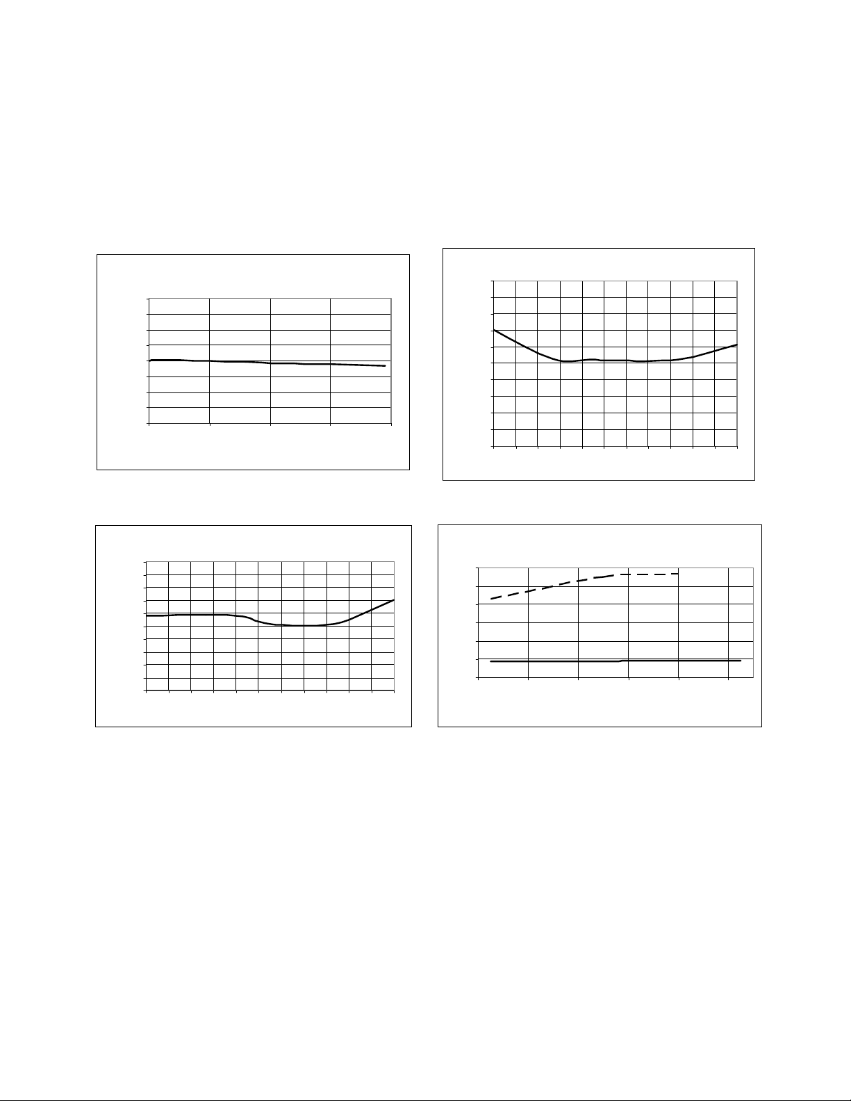
Quad Channel 1°C Temperature Sensor with Hardware Thermal Shutdown and 1.8V SMBus Communications
Temperature Error vs. Filter Capacitor
(2N3904, TA = 27°C, T
DIODE
= 27°C, VDD = 3.3V)
-1.0
-0.8
-0.5
-0.3
0.0
0.3
0.5
0.8
1.0
0 1000 2000 3000 4000
Filter Capacitor (pF)
Temperature Error (°C)
Temperature Error vs. Ambient Temperature
(2N3904, T
DIODE
= 42.5°C, VDD = 3.3V)
-1.0
-0.8
-0.6
-0.4
-0.2
0.0
0.2
0.4
0.6
0.8
1.0
-40 -25 -10 5 20 35 50 65 80 95 110 125
Ambient Temperature (°C)
Temperature Error (°C)
Temperature Error vs. External Diode Temperature
(2N3904, TA = 42.5°C, VDD = 3.3V)
-1.0
-0.8
-0.6
-0.4
-0.2
0.0
0.2
0.4
0.6
0.8
1.0
-40 -25 -10 5 20 35 50 65 80 95 110 125
External Diode Temperature (°C)
Temperature Error (°C)
Temperature Error vs. CPU Temperature
Typical 65 nm CP U from major vendor
(TA = 27°C, VDD = 3.3V, BETA = 011, C
FILTER
= 470pF)
-1
0
1
2
3
4
5
20 40 60 80 100 120
CP U Temp erat u re (°C )
Temperature Error (°C)
Beta Compensation
Disabled
Beta Compensation Enabled
Datasheet
Chapter 7 Typical Operating Curves
Revision 1.0 (07-11-13) 44 SMSC EMC1188
DATASHEET
Page 45
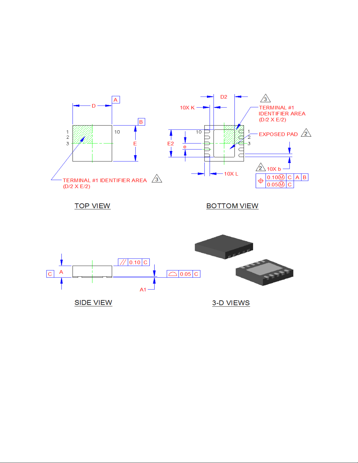
Quad Channel 1°C Temperature Sensor with Hardware Thermal Shutdown and 1.8V SMBus Communications
Chapter 8 Package Information
Datasheet
Figure 8.1 10-Pin DFN Package Drawing
SMSC EMC1188 45 Revision 1.0 (07-11-13)
DATASHEET
Page 46
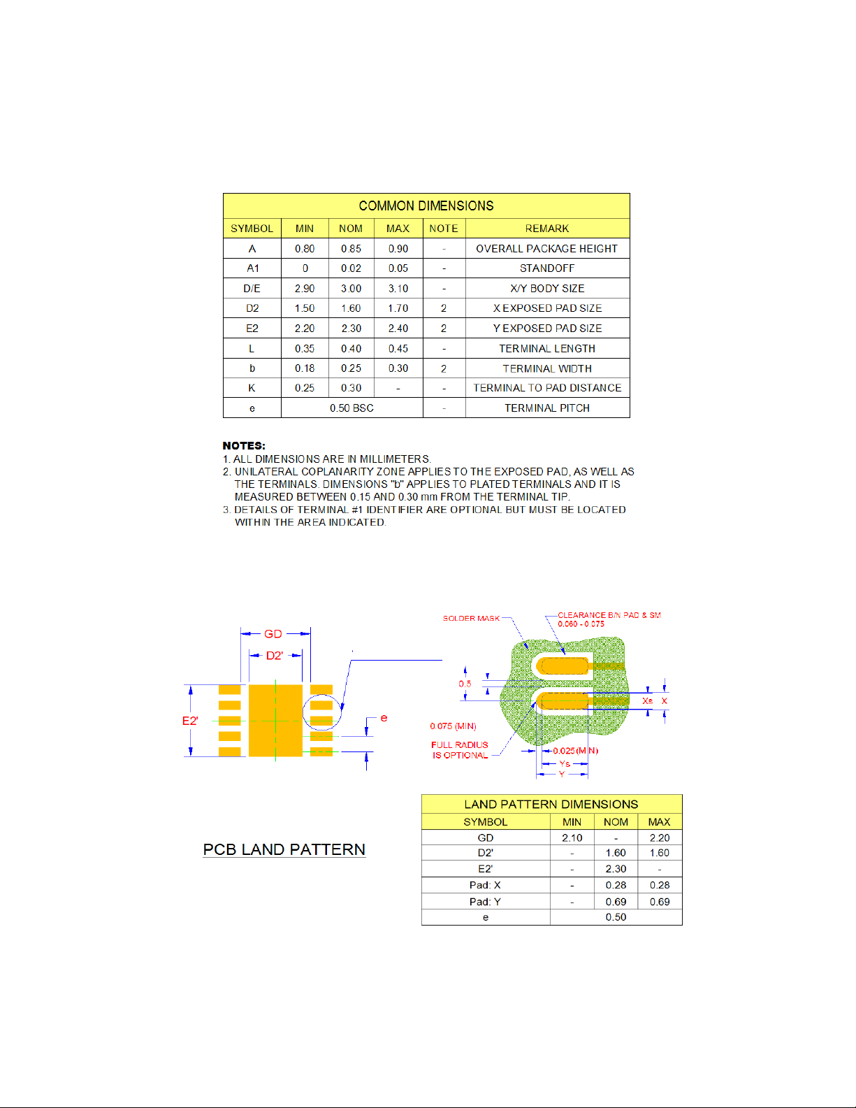
Quad Channel 1°C Temperature Sensor with Hardware Thermal Shutdown and 1.8V SMBus Communications
Datasheet
8.1 Package Markings
Figure 8.2 10-Pin DFN Package Dimensions
Figure 8.3 10 Pin DFN PCB Footprint
The EMC1188 devices will be marked as shown in Figure 8.4.
Revision 1.0 (07-11-13) 46 SMSC EMC1188
DATASHEET
Page 47

Quad Channel 1°C Temperature Sensor with Hardware Thermal Shutdown and 1.8V SMBus Communications
BOTTOM
LINE 1: Device code, first 2 of last 6
digits of lot number
LINE 2: Last 4 digits of lot number
TOP
ex
PIN 1
BOTTOM MARKING IS NOT ALLOWED
4 3 L L
L L L L
Datasheet
Figure 8.4 EMC1188-1 10-Pin DFN Package Marking s
SMSC EMC1188 47 Revision 1.0 (07-11-13)
DATASHEET
Page 48

Quad Channel 1°C Temperature Sensor with Hardware Thermal Shutdown and 1.8V SMBus Communications
Datasheet
Chapter 9 Datasheet Revision History
T able 9.1 Customer Revision History
REVISION LEVEL & DATE SECTION/FIGURE/ENTRY CORRECTION
Rev. 1.0 (07-11-13) Formal document release
Revision 1.0 (07-11-13) 48 SMSC EMC1188
DATASHEET
 Loading...