

Page 1

HV9861A
LED Driver with Average-Mode Constant Current Control
Features
• Fast average current control
• Programmable constant off-time switching
• PWM / linear dimming input
• Output short circuit protection with skip mode
• Ambient operating temperature -40°C to +125°C
• Pin-compatible with the HV9910B and HV9961
Applications
• DC/DC or AC/DC LED driver applications
• LED back-light driver for LCD displays
• General purpose constant current source
• LED signage and displays
• Architectural and decorative LED lighting
• LED street lighting
Description
HV9861A is a patented, average-mode, constant-current control, LED driver IC operating in a constant offtime mode. Unlike the HV9910B, this control IC does
not produce a peak-to-average error, which therefore
greatly improves the accuracy, line and load regulation
of the LED current without any need for loop compensation or high-side current sensing. The output LED
current accuracy is ±3%.
The IC is equipped with a current limit comparator for
hiccup-mode output short circuit protection. Internal
over-temperature protection is provided. The internally
regulated voltage (V
The IC can be powered from a 15 - 450V supply. A
PWM dimming input is provided that accepts an external control TTL-compatible signal. The output current
can be programmed by an internal 270mV reference,
or controlled externally through a 0 - 1.5V dimming
input.
HV9861A is pin-to-pin compatible with the HV9910B
and HV9961, and can be used as a drop-in replacement for many applications to improve the LED current
accuracy and regulation.
) for the HV9861A is 7.5V.
DD
2014 Microchip Technology Inc. DS20005333A-page 1
Page 2

HV9861A
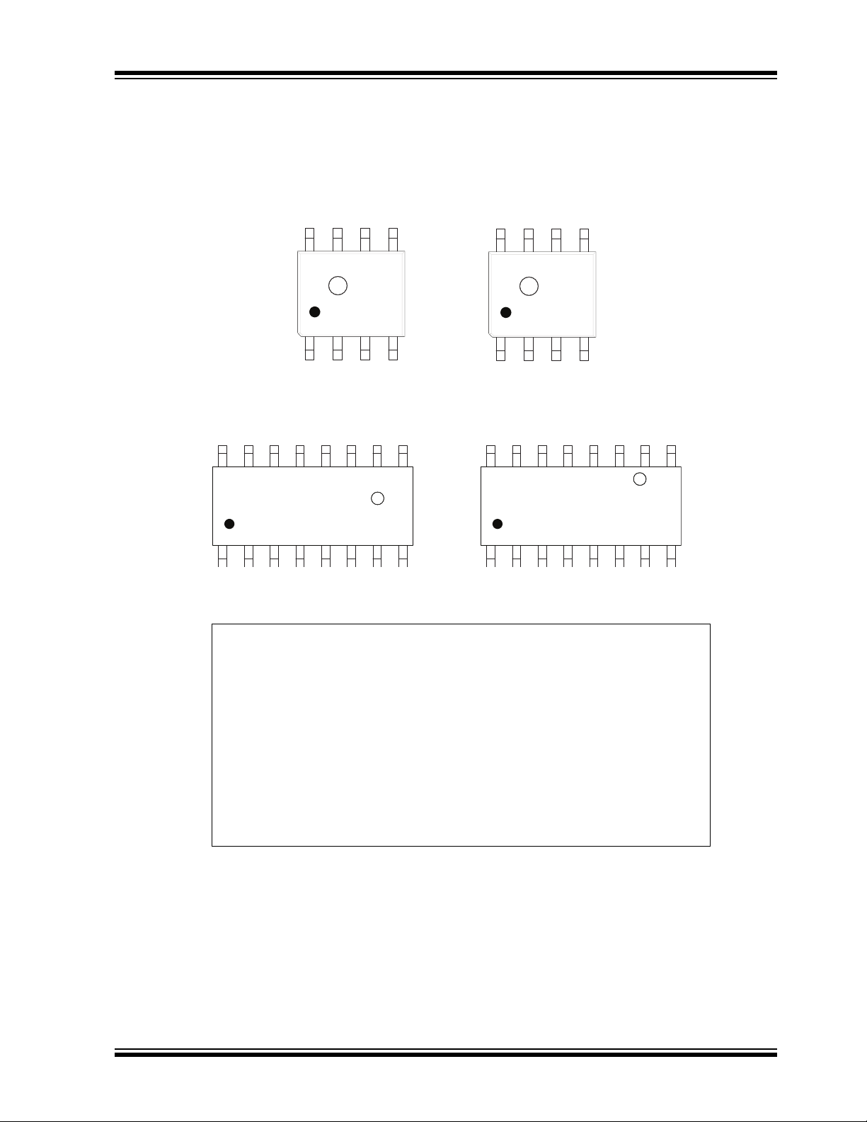
8-Lead SOIC
16-Lead SOIC
See Ta bl e 2 -1 for pin information
PWMD
VDD
LD
GATE
CS
RT
VIN
HV9861A
15VDC to
450VDC
Sets
LED
Current
LED
Load
GND
R
CS
R
T
Package Types
1
VIN
2
CS
3
GND
4
GATE
Typical Application Circuit
8
7
6
5
RT
LD
VDD
PWMD
VIN
NC
NC
CS
GND
NC
NC
GATE
16
15
14
13
12
11
10
9
NC
NC
RT
LD
VDD
NC
NC
PWMD
1
2
3
4
5
6
7
8
DS20005333A-page 2 2014 Microchip Technology Inc.
Page 3

1.0 ELECTRICAL CHARACTERISTICS
ABSOLUTE MAXIMUM RATINGS
VIN to GND...................................................... -0.5V to +470V
V
to GND.......................................................................12V
DD
LD, PWMD, GATE to GND.....................-0.3V to (V
CS, RT to GND .............................................. ....-0.3V to 5.0V
Operating temperature..................................-40°C to +125°C
Storage temperature .....................................-65°C to +150°C
Continuous power dissipation (T
8-lead SOIC ...............................................650 mW
16-lead SOIC ...........................................1000 mW
Note: Stresses above those listed under “Absolute Maximum
Ratings” may cause permanent damage to the device. This is
a stress rating only and functional operation of the device at
those or any other conditions, above those indicated in the
operational listings of this specification, is not implied. Exposure to maximum rating conditions for extended periods may
affect device reliability.
= +25°C)
A
1.1 ELECTRICAL SPECIFICATIONS
+ 0.3V)
DD
HV9861A
TABLE 1-1: ELECTRICAL CHARACTERISTICS (SHEET 1 OF 2)
1
Symbol Parameter Note Min Typ Max Units Conditions
Input
V
I
INSD
INDC
Input DC supply voltage
2
range
Shut-down mode supply
current
3
15 - 450 V DC input voltage
3
- 0.5 1.1 mA Pin PWMD to GND
Internal Regulator
V
DD
V
DD
, load Load regulation of V
V
DD
UVLO
UVLO
V
DD(UV)VDD
I
IN,MAX
Internally regulated voltage - 7.25 7.50 8.20 V 500pF at GATE; RT = 226k
= 15 - 450V,
V
, line Line regulation of V
V
under-voltage lockout
DD
threshold
under-voltage lockout
V
DD
hysteresis
voltage margin
Maximum input current
(limited by UVLO)
DD
DD
---1V
---100mV
3
6.45 - - V VIN rising
--500-mVV
3
500 - - mV V
4
3.5 - -
4
1.5 - - VIN = 15V, TA = 125°C
mA
IN
500pF at GATE; RT = 226k
I
DD(ext)
500pF at GATE; RT = 226k
falling
IN
DD(UV)
VIN = 15V, TA = 25°C
PWM Dimming
V
V
EN(lo)
EN(hi)
I
EN
PWMD input low voltage
PWMD input high voltage
Internal pull-down current at
PWMD
3
3
-8.5-13.5AV
--0.8VV
IN
2.2 - - V VIN = 15 - 450V
PWMD
= 15 - 450V
= 0 - 1mA,
= VDD - UVLO
= 0.8V
2014 Microchip Technology Inc. DS20005333A-page 3
Page 4

HV9861A
TABLE 1-1: ELECTRICAL CHARACTERISTICS (CONTINUED) (SHEET 2 OF 2)
Symbol Parameter Note Min Typ Max Units Conditions
Average Current Sense Logic
V
CS
A
V(LD)
A
V
V
LD(OFFSET)
V
CS(TEMP)
V
LD(OFF)
V
LD(OFF)
T
BLANK
T
ON(min)
D
MAX
Short Circuit Protection
V
CS
T
DELAY
T
HICCUP
T
ON(min)
TOFF Timer
T
OFF
GATE Driver
I
SOURCE
I
SINK
t
RISE
t
FALL
Over-Temperature Protection
T
SD
T
1 Specifications are T
2 Also limited by package-power dissipation limit; Whichever is lower.
3 Applies over the full operating ambient temperature range of -40°C < T
4 For design guidance only
Current sense reference
voltage
- 262 - 280 mV
LD-to-CS voltage ratio - 0.175 - 0.182 -
•
LD-to-CS voltage offset - -10 - 10 mV
CS threshold temp regulation
4
--5mV
Offset = V
VLD = 1.2V
LD input voltage, shutdown - - 150 - mV VLD falling
LD input voltage, enable - - 200 - mV VLD rising
Current sense blanking
interval
3
140 - 290 ns
Minimum on-time - - - 760 ns CS = VCS + 30mV
Maximum steady-state duty
cycle
Hiccup threshold voltage
Current limit delay CS-toGATE
3
80 - - %
3
410 - 510 mV
---150nsCS = V
Reduction in output LED current may occur beyond this
duty cycle
Short circuit hiccup time - 400 - 850 s
Minimum on-time (short circuit) - - - 430 ns C S = 4V
Off-time
-324048
- 8 10 12 R
s
R
Sourcing current - 0.165 - - A V
Sinking current - 0.165 - - A V
Output rise time - - 30 50 ns C
Output fall time - - 30 50 ns C
Shut-down temperature
Hysteresis
SD
= 25°C, VIN = 15V, VLD = VDD, PWMD = VDD unless otherwise noted.
A
4
128 140 - °C ---
4
- 20 - °C ---
< +125°C.
A
CS
= 1M
T
= 226k
T
= 0V, VDD = 7.5V
GATE
= VDD, VDD = 7.5V
GATE
= 500pF, VDD = 7.5V
GATE
= 500pF, VDD = 7.5V
GATE
1
- (A
CS
+ 30mV
V(LD)
• VLD);
TABLE 1-2: THERMAL RESISTANCE
Package θja
8-Lead SOIC 101°C/W
16-Lead SOIC 83°C/W
DS20005333A-page 4 2014 Microchip Technology Inc.
Page 5

2.0 PIN DESCRIPTION
The locations of the pins are listed in Package Types.
TABLE 2-1: PIN DESCRIPTION
Pin #
8-Lead SOIC 16-Lead SOIC
1 1 VIN Input of a 15 - 450V linear regulator.
24CS
35GND
4 8 GATE Output GATE driver for an external N-channel power MOSFET.
59PWMD
612VDD
713LD
814RT
-
2, 3, 6, 7, 10,
11, 15, 16
Function Description
Current sense pin used to sense the FET current by means of an
external sense resistor.
Ground return for all internal circuitry. This pin must be electrically
connected to the ground of the power train.
PWM-dimming input of the IC. When this pin is pulled to GND, the
gate driver is turned off. When the pin is pulled high, the gate driver
operates normally.
Power supply pin for all internal circuits. It must be bypassed with a
low ESR capacitor to GND (at least 0.1F).
Linear-dimming input. Sets the current sense threshold as long as
the voltage at this pin is less than 1.5V. If voltage at LD falls below
150mV, the GATE output is disabled. The GATE signal recovers at
200mV at LD.
A resistor connected between this pin and GND programs the
GATE off-time.
NC
No connection.
HV9861A
2014 Microchip Technology Inc. DS20005333A-page 5
Page 6
HV9861A
T
OFF
s
R
T
k
25
------------------- - 0.3+=
I
LED
0.27V
R
CS
--------------- -=
I
LED
VLD0.18
R
CS
-------------------------=
L
V
OMAXTOFF
0.4 I
O
------------------------------------ -=
3.0 APPLICATION INFORMATION
Peak-current control (as in the HV9910B) of a buck
converter is the most economical and simple way to
regulate its output current. However, this method suffers accuracy and regulation problems that arise from
the so-called peak-to-average current error, contributed to by the current ripple in the output inductor and
the propagation delay in the current-sense comparator.
The full inductor-current signal is unavailable for direct
sensing at the ground potential in a buck converter
when the control switch is referenced to the same
ground potential. While it is very simple to detect the
peak current in the switch, controlling the average
inductor current is usually implemented by level translating the sense signal from the positive supply rail.
Though this is practical for relatively low input voltage,
this type of average-current control may become
excessively complex and expensive in off line AC or
other high-voltage DC applications.
HV9861A employs a patented control scheme, achieving fast and very accurate control of average current in
the buck inductor through sensing the switch current
only. No compensation of the current-control loop is
required. The LED current response to PWMD input is
similar to that of the HV9910B. The inductor-current ripple amplitude does not affect this control scheme significantly. Therefore, the LED current is independent of
the variation in inductance, switching frequency, or output voltage. Constant off-time control of the buck converter is used for stability and to improve the LEDcurrent regulation over a wide range of input voltages.
(Note that, unlike the HV9910B, this IC does not support the constant-frequency mode of operation.)
3.1 OFF Timer
The timing resistor connected to RT determines the offtime of the gate driver, and it must be wired to GND.
Wiring this resistor to GATE as with the HV9910B is no
longer supported. The equation governing the off-time
of the GATE output is given by:
Within the range of 30k R
3.2 Average Current Control Feedback and Output Short Circuit Protection
The current through the switching MOSFET source is
averaged and used to give constant-current feedback.
This current is detected using a sense resistor at the
1.0M.
T
CS pin. The feedback operates in a fast open-loop
mode. No compensation is required. Output current is
programmed simply as:
When the voltage at the LD input V
1.5V. Other-
LD
wise:
The above equations are only valid for continuous conduction of the output inductor. It is a good practice to
design the inductor such that the switching ripple current in it is 30~40% of its average peak-to-peak, full
load, DC current. Hence, the recommended inductance
can be calculated as:
The duty-cycle range of the current control feedback is
limited to D 0.8. A reduction in the LED current may
occur when the LED string voltage V
is greater than
O
80% of the input voltage VIN of the HV9861A LED
driver.
Reducing the output LED voltage VO below V
VIN • D
, where D
MIN
= 760ns/(T
MIN
+760ns), may
OFF
O(MIN)
=
also result in the loss of regulation of the LED current.
However, this condition causes an increase in the LED
current and can potentially trip the short-circuit protection comparator.
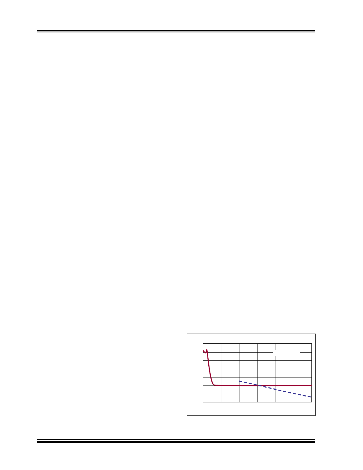
A typical output characteristic of the HV9861A LED
driver is shown in Figure 3-1. The corresponding
HV9910B characteristic is given for comparison.
FIGURE 3-1: TYPICAL OUTPUT
CHARACTERISTIC OF AN
HV9861A LED DRIVER
0.60
0.55
0.50
0.45
0.40
0.35
LED Current (A)
0.30
0.25
0 10 20 30 40 50 60
Output Characteristics
VIN = 170VDC
HV9861A
HV9910B
Output Voltage (V)
DS20005333A-page 6 2014 Microchip Technology Inc.
Page 7
HV9861A
650μs
0.45V/R
CS
0 0.2 0.4 0.6 0.8 1.0 1.2 1.4 1.6
0.40
0.35
0.30
0.25
0.20
0.15
0.10
0.05
0
LED Current (A)
LD (V)
LD Response Characteristics
V
IN MAX
T
JMAXTA
–
R
JA–
IIN
------------------------------ - 330V==
IIN1.0mA QGfs+
The short circuit protection comparator trips when the
voltage at CS exceeds 0.45V. When this occurs, the
GATE off-time T
= 650µs is generated to prevent
HICCUP
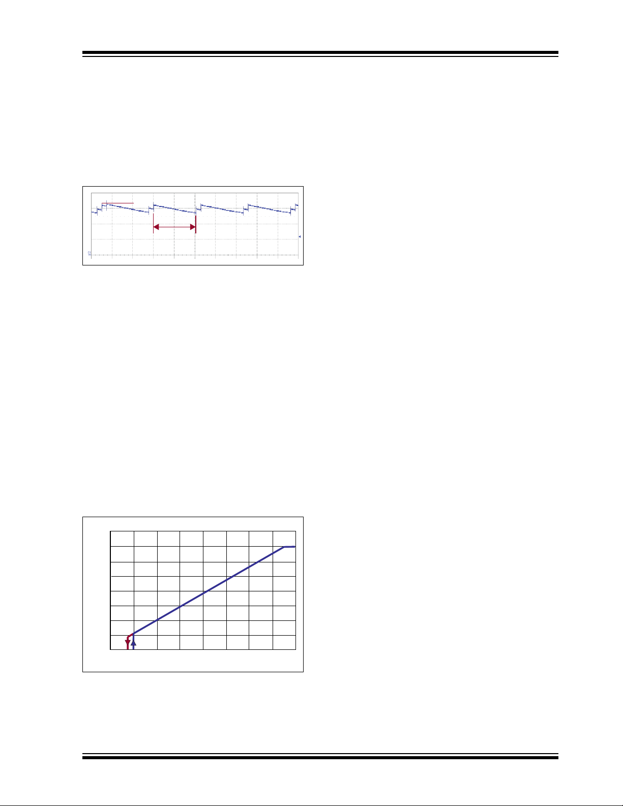
stair-casing of the inductor current, and potentially its
saturation, due to insufficient output voltage. The typical short-circuit current is shown in the waveform of
Figure 3-2.
FIGURE 3-2: SHORT-CIRCUIT
INDUCTOR CURRENT
A leading-edge blanking delay is provided at CS to prevent false triggering of the current feedback and the
short circuit protection.
3.3 Linear Dimming
When the voltage at LD falls below 1.5V, the internal
270mV reference to the constant-current feedback
becomes overridden by VLD • 0.18. As long as the current in the inductor remains continuous, the LED current is given by the equation in Section 3.2. However,
when V
becomes disabled. The GATE signal recovers, when
V
LD
tions to be able to shut the LED lamp off with the same
signal input that controls the brightness. The typical linear dimming response is shown in Figure 3-3.
FIGURE 3-3: TYPICAL LINEAR DIMMING
falls below 150mV, the GATE output
LD
exceeds 200mV. This is required in some applica-
RESPONSE OF AN
HV9861A LED DRIVER
3.4 Input Voltage Regulator
HV9861A can be powered directly from a 15 – 450VDC
supply through its VIN input. When this voltage is
applied at the VIN pin, the HV9861A maintains a constant 7.5V level at VDD. This voltage can be used to
power the IC and external circuitry connected to VDD
within the rated maximum current or within the thermal
ratings of the package, whichever limit is lower. The
VDD pin must be bypassed by a low ESR capacitor to
provide a low impedance path for the high frequency
current of the GATE output. The HV9861A can also be
powered through the VDD pin directly with a voltage
greater than the internally regulated 7.5V, but less than
12V.
Despite the instantaneous voltage rating of 450V, continuous voltage at VIN is limited by the power dissipation in the package. For example, when these ICs draw
= 3.0mA from the VIN input, and the 8-lead SOIC
I
IN
package is used, the maximum continuous voltage at
VIN is limited to the following:
In this instance, the ambient temperature T
maximum working junction temperature T
and the junction-to-ambient thermal resistance R
101°C/W.
In such cases, when it is needed to operate the
HV9861A from a higher voltage, a resistor or a Zener
diode can be added in series with the VIN input to divert
some of the power loss from the IC. In the above example, using a 100V Zener diode will allow the circuit to
work up to 430V. The input current drawn from the VIN
pin is represented by the following equation:
= 25°C, the
A
= 125°C,
J(MAX)
,JA
=
The linear dimming input could also be used for “mixedmode” dimming to expand the dimming ratio. In such
case a pulse-width modulated signal of a measured
amplitude below 1.5V should be applied at LD.
2014 Microchip Technology Inc. DS20005333A-page 7
In the above equation, f
and Q
is the GATE charge of the external FET
G
is the switching frequency,
S
obtained from the manufacturer’s data sheet.
3.5 GATE Output
The GATE output of HV9861A is used to drive an external MOSFET. The gate charge, Q
MOSFET should be less than 25nC for switching frequencies 100kHz and less than 15nC for switching
frequencies >100kHz.
, of the external
G
Page 8
HV9861A
CH2 (red): PWMD
CH4 (green): Inductor Current
CH3 (blue): Same as HV9910B, for comparison
R Q
S Q
T
OFF
Timer
Latch
Enable
Blanking
0.45V
min (V
LD
•
0.18, 0.27V)
650μs
Current
Mirror
i
Regulator
VIN
LD
CS
GND
VDD
GATE
PWMD
RT
UVLO
POR
0.15/0.20V
Average Current
Control Logic
OUT
Auto-REF
HV9861A
CLK
IN
+
-
+
-
+
-
11μA
3.6 PWM Dimming
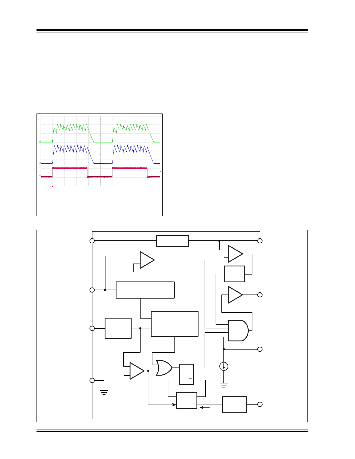
Due to the fast open-loop response of the averagemode, current-control loop of the HV9861A, the PWM
dimming performance nearly matches that of the
HV9910B. The inductor current waveform comparison
is shown in Figure 3-4.
FIGURE 3-4: TYPICAL PWM DIMMING
RESPONSE OF AN
HV9861A LED DRIVER
The rising and falling edges are limited by the current
slew rate in the inductor. The first switching cycle is terminated upon reaching the 270mV (VLD • 0.18) level at
CS. The circuit is further reaching its steady-state
within 3–4 switching cycles regardless of the switching
frequency.
FIGURE 3-5: FUNCTIONAL BLOCK DIAGRAM
DS20005333A-page 8 2014 Microchip Technology Inc.
Page 9
4.0 PACKAGING INFORMATION
Legend: XX...X Product Code or Customer-specific information
Y Year code (last digit of calendar year)
YY Year code (last 2 digits of calendar year)
WW Week code (week of January 1 is week ‘01’)
NNN Alphanumeric traceability code
Pb-free JEDEC
®
designator for Matte Tin (Sn)
* This package is Pb-free. The Pb-free JEDEC designator ( )
can be found on the outer packaging for this package.
Note: In the event the full Microchip part number cannot be marked on one line, it will
be carried over to the next line, thus limiting the number of available
characters for product code or customer-specific information. Package may or
not include the corporate logo.
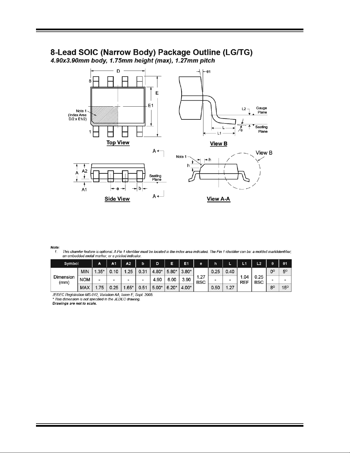
8-lead SOIC
Example
NNN
XX
XXXXXXXX
YYWW
e3
343
LG
HV9861A
1447
e3
16-lead SOIC
XXXXXXXXX
XXXXXXXXXXX
YYWWNNN
e3
Example
HV9861ANG
1447343
e3
4.1 Package Marking Information
HV9861A
2014 Microchip Technology Inc. DS20005333A-page 9
Page 10
HV9861A
Note: For the most current package drawings, see the Microchip Packaging Specification at www.microchip.com/packaging.
DS20005333A-page 10 2014 Microchip Technology Inc.
Page 11
HV9861A
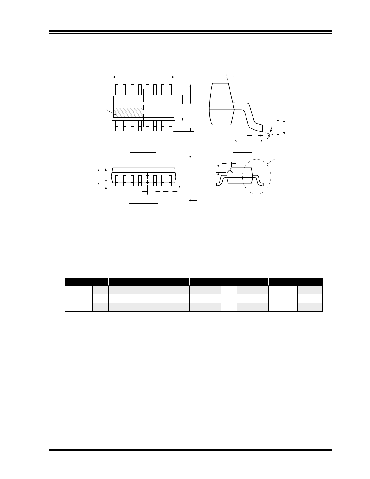
16-Lead SOIC (Narrow Body) Package Outline (NG)
9.90x3.90mm body, 1.75mm height (max), 1.27mm pitch
Symbol A A1 A2 b D E E1 e h L L1 L2 șș
Dimension
(mm)
MIN 1.35* 0.10 1.25 0.31 9.80* 5.80* 3.80*
1.27
BSC
0.25 0.40
1.04
REF
0.25
BSC
0
O5O
NOM - - - - 9.90 6.00 3.90 - - - -
MAX 1.75 0.25 1.65* 0.51 10.00* 6.20* 4.00* 0.50 1.27 8O15
O
JEDEC Registration MS-012, Variation AC, Issue E, Sept. 2005.
7KLVGLPHQVLRQLVQRWVSHFL¿HGLQWKH-('(&GUDZLQJ
Drawings are not to scale.
D
Seating
Plane
Gauge
Plane
L
L1
L2
Top View
Side View
View A-A
View B
View
B
θ1
θ
E1
E
A
A2
A1
A
A
Seating
Plane
e
b
h
h
16
1
Note 1
Note 1
(Index Area
D/2 x E1/2)
Note:
1. 7KLVFKDPIHUIHDWXUHLVRSWLRQDO,ILWLVQRWSUHVHQWWKHQD3LQLGHQWL¿HUPXVWEHORFDWHGLQWKHLQGH[DUHDLQGLFDWHG7KH3LQLGHQWL¿HUFDQEH
DPROGHGPDUNLGHQWL¿HUDQHPEHGGHGPHWDOPDUNHURUDSULQWHGLQGLFDWRU
Note: For the most current package drawings, see the Microchip Packaging Specification at www.microchip.com/packaging.Note: For the most current package drawings, see the Microchip Packaging Specification at www.microchip.com/packaging.
2014 Microchip Technology Inc. DS20005333A-page 11
Page 12

HV9861A
APPENDIX A: REVISION HISTORY
Revision A (December 2014)
• Original Release of this Document.
DS20005333A-page 12 2014 Microchip Technology Inc.
Page 13

PRODUCT IDENTIFICATION SYSTEM
Device: HV9861A= LED Driver with Average-Mode Constant
Current Control
Package: LG = 8-lead SOIC
NG = 16-lead SOIC
Environmental G = Lead (Pb)-free/ROHS-compliant package
Media Type: (blank) = Reel for LG package, Tube for NG package
Examples:
a) HV9861ALG-G: 8-lead SOIC package,
2500/Reel.
b) HV9861ANG-G 16-lead SOIC package,
45/Tube
PAR T N O. X
Device
X
Environmental
XX
Package
Options
Media
-
-
Typ e
To order or obtain information, e.g., on pricing or delivery, refer to the factory or the listed sales office.
HV9861A
2014 Microchip Technology Inc. DS20005333A-page 13
Page 14

Note the following details of the code protection feature on Microchip devices:
YSTEM
CERTIFIEDBYDNV
== ISO/TS16949==
• Microchip products meet the specification contained in their particular Microchip Data Sheet.
• Microchip believes that its family of products is one of the most secure families of its kind on the market today, when used in the
intended manner and under normal conditions.
• There are dishonest and possibly illegal methods used to breach the code protection feature. All of these methods, to our
knowledge, require using the Microchip products in a manner outside the operating specifications contained in Microchip’s Data
Sheets. Most likely, the person doing so is engaged in theft of intellectual property.
• Microchip is willing to work with the customer who is concerned about the integrity of their code.
• Neither Microchip nor any other semiconductor manufacturer can guarantee the security of their code. Code protection does not
mean that we are guaranteeing the product as “unbreakable.”
Code protection is constantly evolving. We at Microchip are committed to continuously improving the code protection features of our
products. Attempts to break Microchip’s code protection feature may be a violation of the Digital Millennium Copyright Act. If such acts
allow unauthorized access to your software or other copyrighted work, you may have a right to sue for relief under that Act.
Information contained in this publication regarding device
applications and the like is provided only for your convenience
and may be superseded by updates. It is your responsibility to
ensure that your application meets with your specifications.
MICROCHIP MAKES NO REPRESENTATIONS OR
WARRANTIES OF ANY KIND WHETHER EXPRESS OR
IMPLIED, WRITTEN OR ORAL, STATUTORY OR
OTHERWISE, RELATED TO THE INFORMATION,
INCLUDING BUT NOT LIMITED TO ITS CONDITION,
QUALITY, PERFORMANCE, MERCHANTABILITY OR
FITNESS FOR PURPOSE. Microchip disclaims all liability
arising from this information and its use. Use of Microchip
devices in life support and/or safety applications is entirely at
the buyer’s risk, and the buyer agrees to defend, indemnify and
hold harmless Microchip from any and all damages, claims,
suits, or expenses resulting from such use. No licenses are
conveyed, implicitly or otherwise, under any Microchip
intellectual property rights.
Trademarks
The Microchip name and logo, the Microchip logo, dsPIC,
FlashFlex, K
PICSTART, PIC
and UNI/O are registered trademarks of Microchip Technology
Incorporated in the U.S.A. and other countries.
FilterLab, Hampshire, HI-TECH C, Linear Active Thermistor,
MTP, SEEVAL and The Embedded Control Solutions
Company are registered trademarks of Microchip Technology
Incorporated in the U.S.A.
Silicon Storage Technology is a registered trademark of
Microchip Technology Inc. in other countries.
Analog-for-the-Digital Age, Application Maestro, BodyCom,
chipKIT, chipKIT logo, CodeGuard, dsPICDEM,
dsPICDEM.net, dsPICworks, dsSPEAK, ECAN,
ECONOMONITOR, FanSense, HI-TIDE, In-Circuit Serial
Programming, ICSP, Mindi, MiWi, MPASM, MPF, MPLAB
Certified logo, MPLIB, MPLINK, mTouch, Omniscient Code
Generation, PICC, PICC-18, PICDEM, PICDEM.net, PICkit,
PICtail, REAL ICE, rfLAB, Select Mode, SQI, Serial Quad I/O,
Total Endurance, TSHARC, UniWinDriver, WiperLock, ZENA
and Z-Scale are trademarks of Microchip Technology
Incorporated in the U.S.A. and other countries.
SQTP is a service mark of Microchip Technology Incorporated
in the U.S.A.
GestIC and ULPP are registered trademarks of Microchip
Technology Germany II GmbH & Co. KG, a subsidiary of
Microchip Technology Inc., in other countries.
All other trademarks mentioned herein are property of their
respective companies.
© 2014, Microchip Technology Incorporated, Printed in the
U.S.A., All Rights Reserved.
Printed on recycled paper.
ISBN: 978-1-63276-871-1
EELOQ, KEELOQ logo, MPLAB, PIC, PICmicro,
32
logo, rfPIC, SST, SST Logo, SuperFlash
QUALITYMANAGEMENTS
DS20005333A-page 14 2014 Microchip Technology Inc.
Microchip received ISO/TS-16949:2009 certification for its worldwide
headquarters, design and wafer fabrication facilities in Chandler and
Tempe, Arizona; Gresham, Oregon and design centers in California
and India. The Company’s quality system processes and procedures
are for its PIC
devices, Serial EEPROMs, microperipherals, nonvolatile memory and
analog products. In addition, Microchip’s quality system for the design
and manufacture of development systems is ISO 9001:2000 certified.
®
MCUs and dsPIC® DSCs, KEELOQ
®
code hopping
Page 15

Worldwide Sales and Service
AMERICAS
Corporate Office
2355 West Chandler Blvd.
Chandler, AZ 85224-6199
Tel: 480-792-7200
Fax: 480-792-7277
Technical Support:
http://www.microchip.com/
support
Web Address:
www.microchip.com
Atlanta
Duluth, GA
Tel: 678-957-9614
Fax: 678-957-1455
Austin, TX
Tel: 512-257-3370
Boston
Westborough, MA
Tel: 774-760-0087
Fax: 774-760-0088
Chicago
Itasca, IL
Tel: 630-285-0071
Fax: 630-285-0075
Cleveland
Independence, OH
Tel: 216-447-0464
Fax: 216-447-0643
Dallas
Addison, TX
Tel: 972-818-7423
Fax: 972-818-2924
Detroit
Novi, MI
Tel: 248-848-4000
Houston, TX
Tel: 281-894-5983
Indianapolis
Noblesville, IN
Tel: 317-773-8323
Fax: 317-773-5453
Los Angeles
Mission Viejo, CA
Tel: 949-462-9523
Fax: 949-462-9608
New York, NY
Tel: 631-435-6000
San Jose, CA
Tel: 408-735-9110
Canada - Toronto
Tel: 905-673-0699
Fax: 905-673-6509
ASIA/PACIFIC
Asia Pacific Office
Suites 3707-14, 37th Floor
Tower 6, The Gateway
Harbour City, Kowloon
Hong Kong
Tel: 852-2943-5100
Fax: 852-2401-3431
Australia - Sydney
Tel: 61-2-9868-6733
Fax: 61-2-9868-6755
China - Beijing
Tel: 86-10-8569-7000
Fax: 86-10-8528-2104
China - Chengdu
Tel: 86-28-8665-5511
Fax: 86-28-8665-7889
China - Chongqing
Tel: 86-23-8980-9588
Fax: 86-23-8980-9500
China - Hangzhou
Tel: 86-571-8792-8115
Fax: 86-571-8792-8116
China - Hong Kong SAR
Tel: 852-2943-5100
Fax: 852-2401-3431
China - Nanjing
Tel: 86-25-8473-2460
Fax: 86-25-8473-2470
China - Qingdao
Tel: 86-532-8502-7355
Fax: 86-532-8502-7205
China - Shanghai
Tel: 86-21-5407-5533
Fax: 86-21-5407-5066
China - Shenyang
Tel: 86-24-2334-2829
Fax: 86-24-2334-2393
China - Shenzhen
Tel: 86-755-8864-2200
Fax: 86-755-8203-1760
China - Wuhan
Tel: 86-27-5980-5300
Fax: 86-27-5980-5118
China - Xian
Tel: 86-29-8833-7252
Fax: 86-29-8833-7256
China - Xiamen
Tel: 86-592-2388138
Fax: 86-592-2388130
China - Zhuhai
Tel: 86-756-3210040
Fax: 86-756-3210049
ASIA/PACIFIC
India - Bangalore
Tel: 91-80-3090-4444
Fax: 91-80-3090-4123
India - New Delhi
Tel: 91-11-4160-8631
Fax: 91-11-4160-8632
India - Pune
Tel: 91-20-3019-1500
Japan - Osaka
Tel: 81-6-6152-7160
Fax: 81-6-6152-9310
Japan - Tokyo
Tel: 81-3-6880- 3770
Fax: 81-3-6880-3771
Korea - Daegu
Tel: 82-53-744-4301
Fax: 82-53-744-4302
Korea - Seoul
Tel: 82-2-554-7200
Fax: 82-2-558-5932 or
82-2-558-5934
Malaysia - Kuala Lumpur
Tel: 60-3-6201-9857
Fax: 60-3-6201-9859
Malaysia - Penang
Tel: 60-4-227-8870
Fax: 60-4-227-4068
Philippines - Manila
Tel: 63-2-634-9065
Fax: 63-2-634-9069
Singapore
Tel: 65-6334-8870
Fax: 65-6334-8850
Taiwan - Hsin Chu
Tel: 886-3-5778-366
Fax: 886-3-5770-955
Taiwan - Kaohsiung
Tel: 886-7-213-7830
Taiwan - Taipei
Tel: 886-2-2508-8600
Fax: 886-2-2508-0102
Thailand - Bangkok
Tel: 66-2-694-1351
Fax: 66-2-694-1350
EUROPE
Austria - Wels
Tel: 43-7242-2244-39
Fax: 43-7242-2244-393
Denmark - Copenhagen
Tel: 45-4450-2828
Fax: 45-4485-2829
France - Paris
Tel: 33-1-69-53-63-20
Fax: 33-1-69-30-90-79
Germany - Dusseldorf
Tel: 49-2129-3766400
Germany - Munich
Tel: 49-89-627-144-0
Fax: 49-89-627-144-44
Germany - Pforzheim
Tel: 49-7231-424750
Italy - Milan
Tel: 39-0331-742611
Fax: 39-0331-466781
Italy - Venice
Tel: 39-049-7625286
Netherlands - Drunen
Tel: 31-416-690399
Fax: 31-416-690340
Poland - Warsaw
Tel: 48-22-3325737
Spain - Madrid
Tel: 34-91-708-08-90
Fax: 34-91-708-08-91
Sweden - Stockholm
Tel: 46-8-5090-4654
UK - Wokingham
Tel: 44-118-921-5800
Fax: 44-118-921-5820
03/25/14
DS20005333A-page 15 2014 Microchip Technology Inc.
 Loading...