

Datasheet dsPIC33FJ32GS406, dsPIC33FJ32GS606, dsPIC33FJ32GS608, dsPIC33FJ32GS610, dsPIC33FJ64GS406 Datasheet
...Page 1

dsPIC33FJ32GS406/606/608/610 and
dsPIC33FJ64GS406/606/608/610
Data Sheet
High-Performance,
16-bit Digital Signal Controllers
2010 Microchip Technology Inc. Preliminary DS70591C
Page 2

Note the following details of the code protection feature on Microchip devices:
• Microchip products meet the specification contained in their particular Microchip Data Sheet.
• Microchip believes that its family of products is one of the most secure families of its kind on the market today, when used in the
intended manner and under normal conditions.
• There are dishonest and possibly illegal methods used to breach the code protection feature. All of these methods, to our
knowledge, require using the Microchip products in a manner outside the operating specifications contained in Microchip’s Data
Sheets. Most likely, the person doing so is engaged in theft of intellectual property.
• Microchip is willing to work with the customer who is concerned about the integrity of their code.
• Neither Microchip nor any other semiconductor manufacturer can guarantee the security of their code. Code protection does not
mean that we are guaranteeing the product as “unbreakable.”
Code protection is constantly evolving. We at Microchip are committed to continuously improving the code protection features of our
products. Attempts to break Microchip’s code protection feature may be a violation of the Digital Millennium Copyright Act. If such acts
allow unauthorized access to your software or other copyrighted work, you may have a right to sue for relief under that Act.
Information contained in this publication regarding device
applications and t he lik e is provided only for your convenience
and may be su perseded by upda t es . It is y our responsibility to
ensure that your application meets with your specifications.
MICROCHIP MAKES NO REPRESENTATIONS OR
WARRANTIES OF ANY KIND WHETHER EXPRESS OR
IMPLIED, WRITTEN OR ORAL, STATUTORY OR
OTHERWISE, RELATED TO THE INFORMATION,
INCLUDING BUT NOT LIMITED TO ITS CONDITION,
QUALITY, PERFORMANCE, MERCHANTABILITY OR
FITNESS FOR PURPOSE. Microchip disclaims all liability
arising from this information and its use. Use of Microchip
devices in life supp ort and/or safety ap plications is entir ely at
the buyer’s risk, and the buyer agrees to defend, indemnify and
hold harmless M icrochip from any and all dama ges, claims,
suits, or expenses re sulting from such use. No licens es are
conveyed, implicitly or otherwise, under any Microchip
intellectual property rights.
Trademarks
The Microchip name and logo, the Microchip logo, dsPIC,
K
EELOQ, KEELOQ logo, MPLAB, PIC, PICmicro, PICSTART,
32
PIC
logo, rfPIC and UNI/O are registered trademarks of
Microchip Technology Incorporated in the U.S.A. and other
countries.
FilterLab, Hampshire, HI-TECH C, Linear Active Thermistor,
MXDEV, MXLAB, SEEVAL and The Embedded Control
Solutions Company are registered trademarks of Microchip
Technology Incorporated in the U.S.A.
Analog-for-the-Digital Age, Application Maestro, CodeGuard,
dsPICDEM, dsPICDEM.net, dsPICworks, dsSPEAK, ECAN,
ECONOMONITOR, FanSense, HI-TIDE, In-Circuit Serial
Programming, ICSP, Mindi, MiWi, MPASM, MPLAB Certified
logo, MPLIB, MPLINK, mTouch, Octopus, Omniscient Code
Generation, PICC, PICC-18, PICDEM, PICDEM.net, PICkit,
PICtail, REAL ICE, rfLAB, Select Mode, Total Endurance,
TSHARC, UniWinDriver, WiperLock and ZENA are
trademarks of Microchip Technology Incorporated in the
U.S.A. and other countries.
SQTP is a service mark of Microchip Technology Incorporated
in the U.S.A.
All other trademarks mentioned herein are property of their
respective companies.
© 2010, Microchip Technology Incorporated, Printed in the
U.S.A., All Rights Reserved.
Printed on recycled paper.
ISBN: 978-1-60932-027-0
Microchip received ISO/TS-16949:2002 certification for its worldwide
headquarters, design and wafer fabrication facilities in Chandler and
Tempe, Arizona; Gresham, Oregon and design centers in California
and India. The Company’s quality system processes and procedures
are for its PIC
devices, Serial EEPROMs, microperipherals, nonvolatile memory and
analog products. In addition, Microchip’s quality system for the design
and manufacture of development systems is ISO 9001:2000 certified.
®
MCUs and dsPIC® DSCs, KEELOQ
®
code hopping
DS70591C-page 2 Preliminary 2010 Microchip Technology Inc.
Page 3

dsPIC33FJ32GS406/606/608/610 and
dsPIC33FJ64GS406/606/608/610
High-Performance, 16-Bit Digital Signal Controllers
Operating Range:
• Up to 40 MIPS operation (at 3.0-3.6V):
- Industrial temperature range (-40°C to +85°C)
- Extended temperature range (-40°C to +125°C)
High-Performance DSC CPU:
• Modified Harvard architecture
• C compiler optimized inst ruction set
• 16-bit wide data path
• 24-bit wide instructions
• Linear program memory addressing up to 4M
instruction words
• Linear data memory addressing up to 64 Kbytes
• 83 base instructions: mostly 1 word/1 cycle
• Two 40-bit accumulators with rounding and
saturation options
• Flexible and powerful addressing modes:
-Indirect
- Modulo
- Bit-Reversed
• Software stack
• 16 x 16 fractional/integer multiply operations
• 32/16 and 16/16 divide operations
• Single-cycle multiply and accumulate:
- Accumulator write back for DSP operations
- Dual data fetch
• Up to ±16-bit shifts for up to 40-bit data
Direct Memory Access (DMA):
• 4-channel hardware DMA
• 1 Kbyte dual ported DMA buff er area (DMA RAM)
to store data transferred via DMA:
- Allows data transfer between RAM and a
peripheral while CPU is executing code (no
cycle steali ng)
• Most peripherals support DMA
Digital I/O:
• Up to 85 programmable digital I/O pi ns
• Wake-up/Interrupt-on-Change for up to 24 pins
• Output pins can drive voltage from 3.0V to 3.6V
• Up to 5V output with open drain configuration
• 5V tolerant digital input pins
• 16 mA source/sink on all PWM pins
On-Chip Flash and SRAM:
• Flash program memory (up to 64 Kbytes)
• Data SRAM (up to 8 Kbytes)
• Boot and General Security for program Flash
Peripheral Features:
• Timer/Counters, up to five 16-bit timers
- Can pair up to make one 32-bit timer
• Input Capture (up to four channels):
- Capture on up, down or both edges
- 16-bit capture input functions
- 4-deep FIFO on each capture
• Output Compare (up to four channels):
- Single or Dual 16-bit Compare mode
- 16-bit Glitchless PWM mode
• 4-wire SPI (up to two modules):
- Framing supports I/O interface to simpl e
codecs
- 1-deep FIFO buffer
- Supports 8-bit and 16-bit data
- Supports all serial clock formats and
sampling modes
2
•I
C™ (up to two modules):
- Supports Full Multi-Master Slave mode
- 7-bit and 10-bit addressing
- Bus collision detection and arbitration
- Integrated signal conditioning
- Slave address masking
2010 Microchip Technology Inc. Preliminary DS70591C-page 3
Page 4

dsPIC33FJ32GS406/606/608/610 and dsPIC33FJ64GS406/606/608/610
Peripheral Features (Continued)
• UART (up to two modules):
- Interrupt on address bit detect
- Interrupt on UART error
- Wake-up on Start bit from Sleep mode
- 4-character TX and RX FIFO buffers
- LIN bus support
©
-IrDA
- High-Speed Baud mode
- Hardware Flow Control with CTS and RTS
• Enhanced CAN (ECAN™ module) 2.0B active:
- Up to eight transmit and up to 32 receive buffers
- 16 receive filters and three masks
- Loopback, Listen Only and Listen All
- Messages modes for diagnostics and bus
- Wake-up on CAN message
- Automatic processing of Remote
- FIFO mode using DMA
- DeviceNet™ addressing support
• Quadrature Encoder Interface (up to 2 modul es ):
- Phase A, Phase B, and index pulse input
- 16-bit up/down position counter
- Count direction status
- Position Measurement (x2 and x 4) mode
- Programmable digital noise filters on inputs
- Alternate 16-bit Timer/Cou nte r mode
- Interrupt on position counter rollover/underflow
encoding and decoding in hardware
monitoring
Transmission Requests
High-Speed PWM Module Features:
• Up to nine PWM generators with up to 18 outputs
• Primary and Secondary time-base
• Individual time base an d duty c ycle fo r each of the
PWM output
• Dead time for rising and falling edges:
- Duty cycle resolution of 1.04 ns
- Dead-time resolution of 1.04 ns
• Phase shift resolution of 1.04 ns
• Frequency resolution of 1.04 ns
• PWM modes supported:
- Standard Edge -Aligned
- True Independent Output
- Complementary
- Center-Aligned
- Push-Pull
-Multi-Phase
- Variable Phase
- Fixed Off-Time
- Current Reset
- Current-Limit
• Independent Fault/Current-Limit inputs
• Output override control
• Special Event Trigger
• PWM capture feature
• Prescaler for input clock
• Dual Trigger from PWM TO ADC
• PWMxL, PWMxH output pin swapping
• On-the-Fly PWM Frequency, Duty cycle and
Phase Shift changes
• Disabling of Individual PWM generators
• Leading-Edge Blanking (LEB) functionality
High-Speed Analog Comparator:
• Up to four Analog Comparators:
- 20 ns response time
- 10-bit DAC for each analog comparator
- DACOUT pin to provide DAC output
- Programmable output polarity
- Selectable input source
- ADC sample and convert capability
• PWM module interface:
- PWM Duty Cycle Control
- PWM Period Control
- PWM Fault Detect
Interrupt Controller:
• 5-cycle latency
• Up to five external interrupts
• Seven programmable priority levels
• Five proc essor exceptions
High-Speed 10-bit ADC:
• 10-bit resolution
• Up to 24 input channels grouped into 12
conversion pairs
• Two internal reference monitoring inputs grouped
into a pair
• Successive Approximation Register (SAR)
converters for parallel conversions of analog pairs:
- 4 Msps for devices with two SARs
- 2 Msps for devices with one SAR
• Dedicated result buffer for each analog channel
• Independent trigger source section for each
analog input conversion pairs
Power Management:
• On-chip 2.5V voltage regulator
• Switch between clock sources in real time
• Idle, Sleep, and Doze modes with fast wake-up
DS70591C-page 4 Preliminary 2010 Microchip Technology Inc.
Page 5

dsPIC33FJ32GS406/606/608/610 and dsPIC33FJ64GS406/606/608/610
CMOS Flash Technology:
• Low-power, high-speed Flash technology
• Fully static design
• 3.3V (±10%) operating voltag e
• Industrial and Extended tempera t ure
• Low power consumption
System Management:
• Flexible clock options :
- External, crystal, resonator, internal RC
- Phase-Locked Loop (PLL) with 120 MHz VCO
- Primary Crystal Os cill ator (OSC) in t he range
of 3 MHz to 40 MHz
- Second ary oscillator (SOSC)
- Internal Low-Power RC (LPRC) o scillator at a
frequency of 32.767 kHz
- Internal Fast RC (FRC) oscillator at a
frequency of 7.37 MHz
• Power-o n Reset (POR )
• Brown-out Reset (BOR)
• Power-up Timer (PWRT)
• Oscillator Start-up Timer (OST)
• Watchdog Timer with its RC oscillator
• Fail-Safe Clock Monitor
• Reset by multiple sources
• In-Circuit Serial Programming™ (ICSP™)
• Reference Oscillator Output
Application Examples:
• AC-to-DC Converters
• Automotive HID
• Battery Chargers
• DC-to-DC Converters
• Digital Lighting
• Induction Cooking
•LED Ballast
• Renewable Power/Pure Sine Wave Inverters
• Uninterruptible Power Supply (UPS)
Packaging:
• 64-pin QFN (9x9x0.9 mm)
• 64-pin TQFP (10x10x1 mm)
• 80-pin TQFP (12x12x1 mm)
• 100-pin TQFP (14x14x1 mm and 12x12x1 mm)
Note: See the dsPIC33FJ32GS406/606/608/
610 and dsPIC33FJ64GS406/606/608/
610 Controller Families table for exact
peripheral features per device.
2010 Microchip Technology Inc. Preliminary DS70591C-page 5
Page 6
dsPIC33FJ32GS406/606/608/610 and dsPIC33FJ64GS406/606/608/610
dsPIC33FJ32GS406/606/608/610 and dsPIC33FJ64GS406/606/608/610 PRODUCT FAMILIES
The device names, pin counts, memory sizes, and
peripheral availability of each device are listed in
Table 1. The following pages show their pinout
diagrams.
TABLE 1: dsPIC33FJ32GS406/606/608/610 and dsPIC33FJ64GS406/606/608/610 CONTROLLER
FAMILIES
ADC
Device
dsPIC33FJ32GS40664324K544212006x20502151658PT,
dsPIC33FJ32GS60664324K544222006x24512261658PT,
dsPIC33FJ32GS60880324K544222008x24512261874PT
dsPIC33FJ32GS610100324K544222009x24512262485PT,
dsPIC33FJ64GS40664648K544212006x20502151658PT,
dsPIC33FJ64GS606 64 64 9K
dsPIC33FJ64GS608 80 64 9K
dsPIC33FJ64GS610 100 64 9K
Note 1: RAM size is inclusive of 1 Kbyte DMA RAM.
Pins
Program Flash Memory (Kbytes)
UART
16-bit Timer
RAM (Bytes)
(1)
(1)
(1)
Input Capture
Output Compare
544222146x24512261658PT,
544222148x24512261874PT
544222149x24512262485PT,
SPI
Quadrature Encoder Interface
ECAN™
PWM
DMA Channels
Analog Compara tor
External Interrupts
C™
2
I
DAC Output
SARs
Sample and Hold (S&H) Circuit
I/O Pins
Packages
Analog-to-Digital Inputs
MR
MR
PF
MR
MR
PF
DS70591C-page 6 Preliminary 2010 Microchip Technology Inc.
Page 7

dsPIC33FJ32GS406/606/608/610 and dsPIC33FJ64GS406/606/608/610
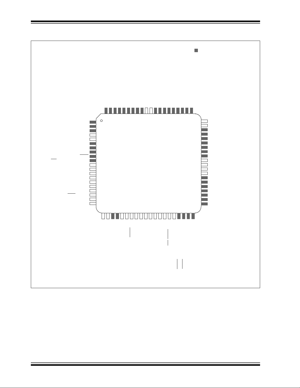
64-Pin TQFP
1
2
3
4
5
6
7
8
9
10
11
12
13
36
35
34
33
32
31
30
29
28
27
26
646362616059585756
14
15
16
171819202122232425
dsPIC33FJ32GS406
PGEC2/SOSCO/T1CK/CN0/RC14
PGED2/SOSCI/T4CK/CN1/RC13
OC1/QEB1/FLT5/RD0
IC4/QEA1/FLT4/INT4/RD11
IC2/FLT2/U1CTS
/INT2/RD9
IC1/FLT1/SYNCI1/INT1/RD8
V
SS
OSC2/REFCLKO/CLKO/RC15
OSC1/CLKIN/RC12
V
DD
SCL1/RG2
U1RTS
/SCK1/INT0/RF6
U1RX/SDI1/RF2
U1TX/SDO1/RF3
PWM3H/RE5
PWM4L/RE6
PWM4H/RE7
SCK2/FLT12/CN8/RG6
SDI2/FLT11/CN9/RG7
SDO2/FLT10/CN10/RG8
MCLR
VSS
VDD
AN3/AINDX1/CN5/RB3
AN2/ASS1
/CN4/RB2
PGEC3/B/AN1/CN3/RB1
PGED3/AN0/CN2/RB0
PWM5H/UPDN1/CN16/RD7
PWM3L/RE4
PWM2H/RE3
PWM2L/RE2
V
CAP/VDDCORE
PWM1L1/FLT8/RE0
RF1
PWM1H1/RE1
OC2/SYNCO2/FLT6/RD1
OC3/FLT7/SYNCI3/RD2
PGEC1/AN6/OCFA/RB6
PGED1/AN7/RB7
AV
DD
AVSS
AN8/U2CTS/RB8
AN9/RB9
TMS/AN10/RB10
TDO/AN11/RB11
V
SS
VDD
TCK/AN12/RB12
TDI/AN13/RB13
AN14/SS1
/U2RTS/RB14
AN15/OCFB/CN12/RB15
U2TX/SCL2/FLT18/CN18/RF5
U2RX/SDA2/FLT17/CN17/RF4
SDA1/RG3
43
42
41
40
39
38
37
44
48
47
46
504951
545352
55
45
SS2
/FLT9/SYNCI2/T5CK/CN11/RG9
AN5/AQEB1/CN7/RB5
AN4/AQEA1/CN6/RB4
IC3/INDX1/FLT3/INT3/RD10
VDD
SYNCI4/RF0
OC4/SYNCO1/RD3
PWM5L/CN15/RD6
PWM6H/CN14/RD5
PWM6L/CN13/RD4
dsPIC33FJ64GS406
= Pins are up to 5V tolerant
Pin Diagrams
2010 Microchip Technology Inc. Preliminary DS70591C-page 7
Page 8
dsPIC33FJ32GS406/606/608/610 and dsPIC33FJ64GS406/606/608/610
64-Pin QFN
PGEC2/SOSCO/T1CK/CN0/RC14
PGED2/SOSCI/T4CK/CN1/RC13
OC1/QEB1/FLT5/RD0
IC4/QEA1/FLT4/INT4/RD11
IC2/FLT2/U1CTS
/INT2/RD9
IC1/FLT1/SYNCI1/INT1/RD8
V
SS
OSC2/REFCLKO/CLKO/RC15
OSC1/CLKIN/RC12
V
DD
SCL1/RG2
U1RTS
/SCK1/INT0/RF6
U1RX/SDI1/RF2
U1TX/SDO1/RF3
PWM3H/RE5
PWM4L/RE6
PWM4H/RE7
SCK2/FLT12/CN8/RG6
SDI2/FLT11/CN9/RG7
SDO2/FLT10/CN10/RG8
MCLR
VSS
VDD
AN3/AINDX1/CN5/RB3
AN2/ASS1
/CN4/RB2
PGEC3/B/AN1/CN3/RB1
PGED3/AN0/CN2/RB0
PWM5H/UPDN1/CN16/RD7
PWM3L/RE4
PWM2H/RE3
PWM2L/RE2
V
CAP/VDDCORE
PWM1L1/FLT8/RE0
RF1
PWM1H1/RE1
OC2/SYNCO2/FLT6/RD1
OC3/FLT7/SYNCI3/RD2
PGEC1/AN6/OCFA/RB6
PGED1/AN7/RB7
AV
DD
AVss
AN8/U2CTS
/RB8
AN9/RB9
TMS/AN10/RB10
TDO/AN11/RB11
V
SS
VDD
TCK/AN12/RB12
TDI/AN13/RB13
AN14/SS1
/U2RTS/RB14
AN15/OCFB/CN12/RB15
U2TX/SCL2/FLT18/CN18/RF5
U2RX/SDA2/FLT17/CN17/RF4
SDA1/RG3
SS2
/FLT9/SYNCI2/T5CK/CN11/RG9
AN5/AQEB1/CN7/RB5
AN4/AQEA1/CN6/RB4
IC3/INDX1/FLT3/INT3/RD10
VDD
SYNCI4/RF0
OC4/SYNCO1/RD3
PWM5L/CN15/RD6
PWM6H/CN14/RD5
PWM6L/CN13/RD4
646362 61 60595857 56 55
2223 24 2526272829 30 31
3
40
39
38
37
36
35
34
33
4
5
7
8
9
10
11
1
2
42
41
6
32
43
54
14
15
16
12
13
17
1819 20 21
45
44
47
46
48
53
52515049
dsPIC33FJ32GS406
dsPIC33FJ64GS406
= Pins are up to 5V tolerant
Note: The metal plane at the bottom of the device is not connected to any pins and is recomm ended t o be connected to
V
SS externally.
Pin Diagrams (Continued)
DS70591C-page 8 Preliminary 2010 Microchip Technology Inc.
Page 9

dsPIC33FJ32GS406/606/608/610 and dsPIC33FJ64GS406/606/608/610
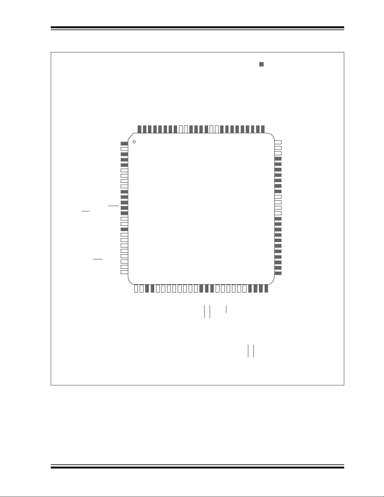
64-Pin TQFP
1
2
3
4
5
6
7
8
9
10
11
12
13
36
35
34
33
32
31
30
29
28
27
26
646362616059585756
14
15
16
171819202122232425
PGEC2/SOSCO/T1CK/CN0/RC14
PGED2/SOSCI/T4CK/CN1/RC13
OC1/QEB1/FLT5/RD0
IC4/QEA1/FLT4/INT4/RD11
IC2/FLT2/U1CTS
/INT2/RD9
IC1/FLT1/SYNCI1/INT1/RD8
V
SS
OSC2/REFCLKO/CLKO/RC15
OSC1/CLKIN/RC12
V
DD
SCL1/RG2
U1RTS
/SCK1/INT0/RF6
U1RX/SDI1/RF2
U1TX/SDO1/RF3
PWM3H/RE5
PWM4L/RE6
PWM4H/RE7
SCK2/FLT12/CN8/RG6
SDI2/FLT11/CN9/RG7
SDO2/FLT10/CN10/RG8
MCLR
VSS
VDD
AN3/CMP2B/AINDX1/CN5/RB3
AN2/CMP1C/CMP2A/ASS1
/CN4/RB2
PGEC3/B/AN1/CMP1B/CN3/RB1
PGED3/AN0/CMP1A/CMP4C/CN2/RB0
PWM5H/UPDN1/CN16/RD7
PWM3L/RE4
PWM2H/RE3
PWM2L/RE2
V
CAP/VDDCORE
PWM1L1/FLT8/RE0
RF1
PWM1H1/RE1
OC2/SYNCO2/FLT6/RD1
OC3/FLT7/SYNCI3/RD2
PGEC1/AN6/CMP3C/CMP4A/OCFA/RB6
PGED1/AN7/CMP4B/RB7
AVdd
AV
SS
AN8/U2CTS/RB8
AN9/DACOUT/RB9
TMS/AN10/RB10
TDO/AN11/EXTREF/RB11
V
SS
VDD
TCK/AN12/CMP1D/RB12
TDI/AN13/CMP2D/RB13
AN14/CMP3D/SS1
/U2RTS/RB14
AN15/CMP4D/OCFB/CN12/RB15
U2TX/SCL2/FLT18/CN18/RF5
U2RX/SDA2/FLT17/CN17/RF4
SDA1/RG3
43
42
41
40
39
38
37
44
48
47
46
504951
545352
55
45
SS2
/FLT9/SYNCI2/T5CK/CN11/RG9
AN5/CMP3B/AQEB1/CN7/RB5
AN4/CMP2C/CMP3A/AQEA1/CN6/RB4
IC3/INDX1/FLT3/INT3/RD10
VDD
SYNCI4/RF0
OC4/SYNCO1/RD3
PWM5L/CN15/RD6
PWM6H/CN14/RD5
PWM6L/CN13/RD4
dsPIC33FJ32GS606
= Pins are up to 5V tolerant
Pin Diagrams (Continued)
2010 Microchip Technology Inc. Preliminary DS70591C-page 9
Page 10
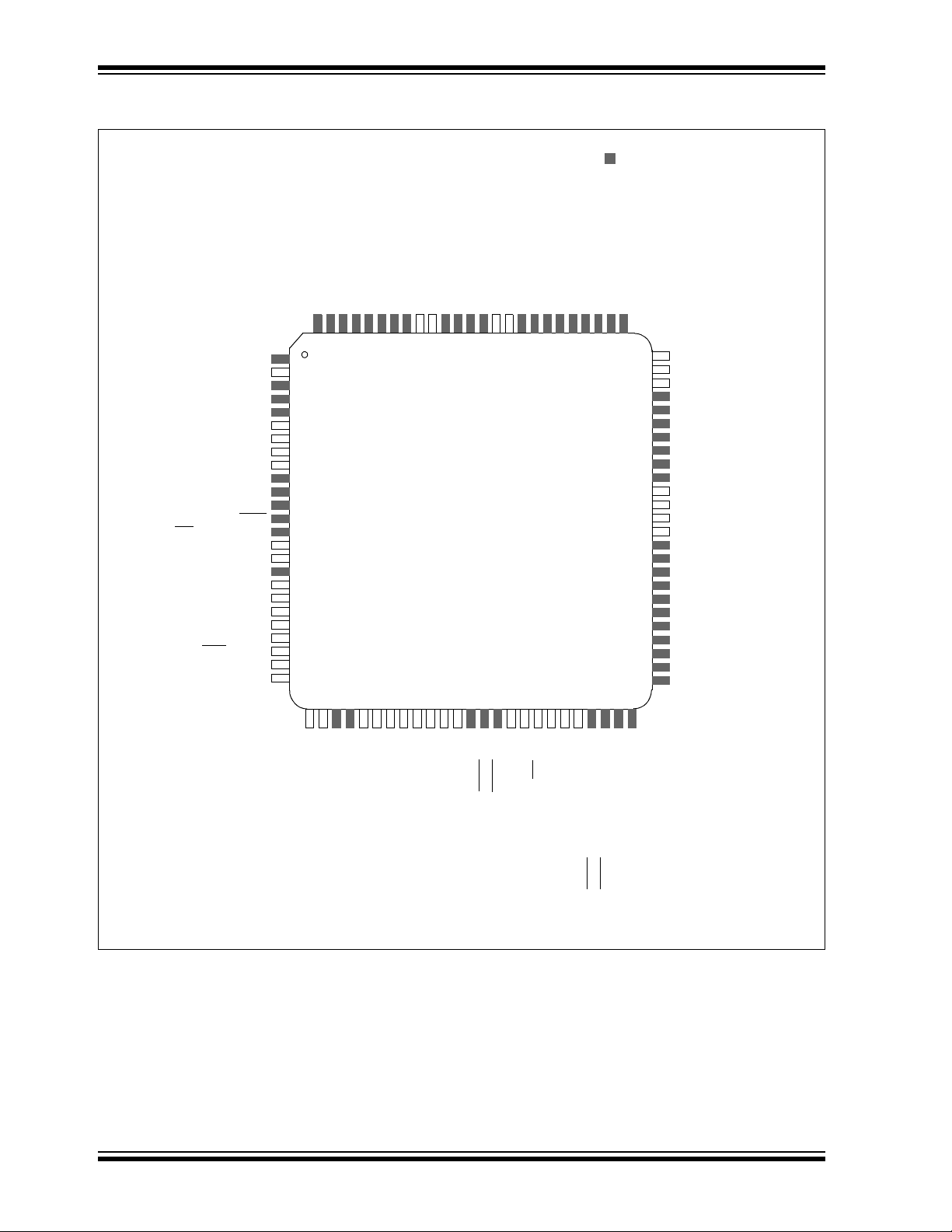
dsPIC33FJ32GS406/606/608/610 and dsPIC33FJ64GS406/606/608/610
64-Pin TQFP
1
2
3
4
5
6
7
8
9
10
11
12
13
36
35
34
33
32
31
30
29
28
27
26
646362616059585756
14
15
16
171819202122232425
PGEC2/SOSCO/T1CK/CN0/RC14
PGED2/SOSCI/T4CK/CN1/RC13
OC1/QEB1/FLT5/RD0
IC4/QEA1/FLT4/INT4/RD11
IC2/FLT2/U1CTS
/INT2/RD9
IC1/FLT1/SYNCI1/INT1/RD8
V
SS
OSC2/REFCLKO/CLKO/RC15
OSC1/CLKIN/RC12
V
DD
SCL1/RG2
U1RTS
/SCK1/INT0/RF6
U1RX/SDI1/RF2
U1TX/SDO1/RF3
PWM3H/RE5
PWM4L/RE6
PWM4H/RE7
SCK2/FLT12/CN8/RG6
SDI2/FLT11/CN9/RG7
SDO2/FLT10/CN10/RG8
MCLR
VSS
VDD
AN3/CMP2B/AINDX1/CN5/RB3
AN2/CMP1C/CMP2A/ASS1
/CN4/RB2
PGEC3/B/AN1/CMP1B/CN3/RB1
PGED3/AN0/CMP1A/CMP4C/CN2/RB0
PWM5H/UPDN1/CN16/RD7
PWM3L/RE4
PWM2H/RE3
PWM2L/RE2
V
CAP/VDDCORE
PWM1L1/FLT8/RE0
C1TX/RF1
PWM1H1/RE1
OC2/SYNCO2/FLT6/RD1
OC3/FLT7/SYNCI3/RD2
PGEC1/AN6/CMP3C/CMP4A/OCFA/RB6
PGED1/AN7/CMP4B/RB7
AVdd
AV
SS
AN8/U2CTS/RB8
AN9/DACOUT/RB9
TMS/AN10/RB10
TDO/AN11/EXTREF/RB11
V
SS
VDD
TCK/AN12/CMP1D/RB12
TDI/AN13/CMP2D/RB13
AN14/CMP3D/SS1
/U2RTS/RB14
AN15/CMP4D/OCFB/CN12/RB15
U2TX/SCL2/FLT18/CN18/RF5
U2RX/SDA2/FLT17/CN17/RF4
SDA1/RG3
43
42
41
40
39
38
37
44
48
47
46
504951
545352
55
45
SS2
/FLT9/SYNCI2/T5CK/CN11/RG9
AN5/CMP3B/AQEB1/CN7/RB5
AN4/CMP2C/CMP3A/AQEA1/CN6/RB4
IC3/INDX1/FLT3/INT3/RD10
VDD
C1RX/SYNCI4/RF0
OC4/SYNCO1/RD3
PWM5L/CN15/RD6
PWM6H/CN14/RD5
PWM6L/CN13/RD4
dsPIC33FJ64GS606
= Pins are up to 5V tolerant
Pin Diagrams (Continued)
DS70591C-page 10 Preliminary 2010 Microchip Technology Inc.
Page 11
dsPIC33FJ32GS406/606/608/610 and dsPIC33FJ64GS406/606/608/610
PGEC2/SOSCO/T1CK/CN0/RC14
PGED2/SOSCI/T4CK/CN1/RC13
OC1/QEB1/FLT5/RD0
IC4/QEA1/FLT4/INT4/RD11
IC2/FLT2/U1CTS
/INT2/RD9
IC1/FLT1/SYNCI1/INT1/RD8
V
SS
OSC2/REFCLKO/CLKO/RC15
OSC1/CLKIN/RC12
V
DD
SCL1/RG2
U1RTS
/SCK1/INT0/RF6
U1RX/SDI1/RF2
U1TX/SDO1/RF3
PWM3H/RE5
PWM4L/RE6
PWM4H/RE7
SCK2/FLT12/CN8/RG6
SDI2/FLT11/CN9/RG7
SDO2/FLT10/CN10/RG8
MCLR
VSS
VDD
AN3/CMP2B/AINDX1/CN5/RB3
AN2/CMP1C/CMP2A/ASS1
/CN4/RB2
PGEC3/B/AN1/CMP1B/CN3/RB1
PGED3/AN0/CMP1A/CMP4C/CN2/RB0
PWM5H/UPDN1/CN16/RD7
PWM3L/RE4
PWM2H/RE3
PWM2L/RE2
V
CAP/VDDCORE
PWM1L1/FLT8/RE0
RF1
PWM1H1/RE1
OC2/SYNCO2/FLT6/RD1
OC3/FLT7/SYNCI3/RD2
PGEC1/AN6/CMP3C/CMP4A/OCFA/RB6
PGED1/AN7/CMP4B/RB7
AV
DD
AVSS
AN8/U2CTS/RB8
AN9/DACOUT/RB9
TMS/AN10/RB10
TDO/AN11/EXTREF/RB11
V
SS
VDD
TCK/AN12/CMP1D/RB12
TDI/AN13/CMP2D/RB13
AN14/CMP3D/SS1
/U2RTS/RB14
AN15/CMP4D/OCFB/CN12/RB15
U2TX/SCL2FLT18//CN18/RF5
U2RX/SDA2/FLT17/CN17/RF4
SDA1/RG3
SS2
/FLT9/SYNCI2/T5CK/CN11/RG9
AN5/CMP3B/AQEB1/CN7/RB5
AN4/CMP2C/CMP3A/AQEA1/CN6/RB4
IC3/INDX1/FLT3/INT3/RD10
VDD
SYNCI4/RF0
OC4/SYNCO1/RD3
PWM5L/CN15/RD6
PWM6H/CN14/RD5
PWM6L/CN13/RD4
64 63 62 6160 59 58 57 56 55
22 23 2425 26 27 28 29 30 31
3
40
39
38
37
36
35
34
33
4
5
7
8
9
10
11
1
2
42
41
6
32
43
54
14
15
16
12
13
17
18 19 2021
45
44
47
46
48
53
52 51 5049
dsPIC33FJ32GS606
64-Pin QFN
= Pins are up to 5V tolerant
Note: The metal plane at the bottom of the device is not connected to any pins and is recommended to be connected to
V
SS externally.
Pin Diagrams (Continued)
2010 Microchip Technology Inc. Preliminary DS70591C-page 11
Page 12

dsPIC33FJ32GS406/606/608/610 and dsPIC33FJ64GS406/606/608/610
64-Pin QFN
PGEC2/SOSCO/T1CK/CN0/RC14
PGED2/SOSCI/T4CK/CN1/RC13
OC1/QEB1/FLT5/RD0
IC4/QEA1/FLT4/INT4/RD11
IC2/FLT2/U1CTS
/INT2/RD9
IC1/FLT1/SYNCI1/INT1/RD8
V
SS
OSC2/REFCLKO/CLKO/RC15
OSC1/CLKIN/RC12
V
DD
SCL1/RG2
U1RTS
/SCK1/INT0/RF6
U1RX/SDI1/RF2
U1TX/SDO1/RF3
PWM3H/RE5
PWM4L/RE6
PWM4H/RE7
SCK2/FLT12/CN8/RG6
SDI2/FLT11/CN9/RG7
SDO2/FLT10/CN10/RG8
MCLR
VSS
VDD
AN3/CMP2B/AINDX1/CN5/RB3
AN2/CMP1C/CMP2A/ASS1
/CN4/RB2
PGEC3/B/AN1/CMP1B/CN3/RB1
PGED3/AN0/CMP1A/CMP4C/CN2/RB0
PWM5H/UPDN1/CN16/RD7
PWM3L/RE4
PWM2H/RE3
PWM2L/RE2
V
CAP/VDDCORE
PWM1L1/FLT8/RE0
C1TX/RF1
PWM1H1/RE1
OC2/SYNCO2/FLT6/RD1
OC3/FLT7/SYNCI3/RD2
PGEC1/AN6/CMP3C/CMP4A/OCFA/RB6
PGED1/AN7/CMP4B/RB7
AV
DD
AVSS
AN8/U2CTS/RB8
AN9/DACOUT/RB9
TMS/AN10/RB10
TDO/AN11/EXTREF/RB11
V
SS
VDD
TCK/AN12/CMP1D/RB12
TDI/AN13/CMP2D/RB13
AN14/CMP3D/SS1
/U2RTS/RB14
AN15/CMP4D/OCFB/CN12/RB15
U2TX/SCL2/FLT18/CN18/RF5
U2RX/SDA2/FLT17/CN17/RF4
SDA1/RG3
SS2
/FLT9/SYNCI2/T5CK/CN11/RG9
AN5/CMP3B/AQEB1/CN7/RB5
AN4/CMP2C/CMP3A/AQEA1/CN6/RB4
IC3/INDX1/FLT3/INT3/RD10
VDD
C1RX/SYNCI4/RF0
OC4/SYNCO1/RD3
PWM5L/CN15/RD6
PWM6H/CN14/RD5
PWM6L/CN13/RD4
64 63 62 61 60 59 5857 56 55
22 23 2425 26 27 28 29 30 31
3
40
39
38
37
36
35
34
33
4
5
7
8
9
10
11
1
2
42
41
6
32
43
54
14
15
16
12
13
17
18 19 2021
45
44
47
46
48
53
52 51 5049
dsPIC33FJ64GS606
= Pins are up to 5V tolerant
Note: The metal plane at the bottom of the device is not connected to any pins and is recomm ended t o be connected to
V
SS externally.
Pin Diagrams (Continued)
DS70591C-page 12 Preliminary 2010 Microchip Technology Inc.
Page 13

dsPIC33FJ32GS406/606/608/610 and dsPIC33FJ64GS406/606/608/610
80-Pin TQFP
727473
7170696867666564636261
20
2
3
4
5
6
7
8
9
10
11
12
13
14
15
16
50
49
48
47
46
45
44
21
41
40
39
38
37
36
35
34
2324252627282930313233
dsPIC33FJ32GS608
17
18
19
75
1
57
56
55
54
53
52
51
60
59
58
43
42
767877
79
22
80
QEA2/RD12
PWM7H/OC4/SYNCO1/RD3
OC3/FLT7/RD2
OC2/SYNCO2/FLT6/RD1
PWM2L/RE2
PWM1H1/RE1
PWM1L1/FLT8/RE0
INDX2SYNCI4//RG0
QEB2/RG1
RF1
RF0
PWM3L/RE4
PWM2H/RE3
PWM5H/UPDN1/CN16/RD7
PWM6H/CN14/RD5
OC1/QEB1/FLT5/RD0
IC4/QEA1/FLT4/RD11
IC2/FLT2/RD9
IC1/FLT1/SYNCI1/RD8
SDA2/INT4/FLT19/RA15
IC3/INDX1/FLT3/RD10
SCL2/INT3/FLT20/RA14
V
SS
OSC1/CLKIN/RC12
V
DD
SCL1/RG2
U1RX/RF2
U1TX/RF3
PGEC2/SOSCO/T1CK/CN0/R C14
PGED2/SOSCI/T4CK/CN1/RC13
PWM8H/RA10
PWM8L/RA9
AV
DD
AVSS
AN8/U2CTS/RB8
AN9/DACOUT/RB9
AN10/RB10
AN11/EXTREF/RB11
V
DD
U2RX/FLT17/CN17/RF4
U1RTS
/FLT16/SYNCI2/CN21/RD15
U2TX/FLT18/CN18/RF5
PGEC1/AN6CMP3C/CMP4A//OCFA/RB6
PGED1/AN7/CMP4B/RB7
PWM4H/RE7
SCK2/FLT12/CN8/RG6
SDI2/FLT11/CN9/RG7
SDO2/FLT10/CN10/RG8
MCLR
SS2/FLT9/T5CK/CN11/RG9
AN4/CMP2C/CMP3A/AQEA1/CN6/RB4
AN3/CMP2B/AINDX1/CN5/RB3
AN2/CMP1C/CMP2A/ASS1
/CN4/RB2
PGEC3/AN1/CMP1B/CN3/RB1
PGED3/AN0/CMP1A/CMP4C/CN2/RB0
V
SS
VDD
PWM3H/RE5
PWM4L/RE6
TDO/FLT14/INT2/RE9
TMS/FLT13/INT1/RE8
TCK/AN12/CMP1D/RB12
TDI/AN13/CMP2D/RB13
AN14/CMP3D/SS1
/U2RTS/RB14
AN15/CMP4D/OCFB/CN12/RB15
V
DD
VCAP/VDDCORE
PWM6L/CN13/RD4
PWM7L/CN19/RD13
SDA1/RG3
SDI1/RF7
SDO1/RF8
AN5/CMP3B/AQEB1/CN7/RB5
VSS
OSC2/REFCLKO/CLKO/RC15
PWM5L/CN15/RD6
SCK1/INT0/RF6
U1CTS/FLT15/SYNCI3/CN20/RD14
AN16/T2CK/RC1
AN17/T3CK/RC2
= Pins are up to 5V tolerant
Pin Diagrams (Continued)
2010 Microchip Technology Inc. Preliminary DS70591C-page 13
Page 14
dsPIC33FJ32GS406/606/608/610 and dsPIC33FJ64GS406/606/608/610
80-Pin TQFP
727473
7170696867666564636261
20
2
3
4
5
6
7
8
9
10
11
12
13
14
15
16
50
49
48
47
46
45
44
21
41
40
39
38
37
36
35
34
2324252627282930313233
17
18
19
75
1
57
56
55
54
53
52
51
60
59
58
43
42
767877
79
22
80
QEA2/RD12
PWM7H/OC4/SYNCO1/RD3
OC3/FLT7/RD2
OC2/SYNCO2/FLT6/RD1
PWM2L/RE2
PWM1H1/RE1
PWM1L1/FLT8/RE0
INDX2SYNCI4//RG0
QEB2/RG1
C1TX/RF1
C1RX/RF0
PWM3L/RE4
PWM2H/RE3
PWM5H/UPDN1/CN16/RD7
PWM6H/CN14/RD5
OC1/QEB1/FLT5/RD0
IC4/QEA1/FLT4/RD11
IC2/FLT2/RD9
IC1/FLT1/SYNCI1/RD8
SDA2/INT4/FLT19/RA15
IC3/INDX1/FLT3/RD10
SCL2/INT3/FLT20/RA14
V
SS
OSC1/CLKIN/RC12
V
DD
SCL1/RG2
U1RX/RF2
U1TX/RF3
PGEC2/SOSCO/T1CK/CN0/R C14
PGED2/SOSCI/T4CK/CN1/RC13
PWM8H/RA10
PWM8L/RA9
AV
DD
AVSS
AN8/U2CTS/RB8
AN9/DACOUT/RB9
AN10/RB10
AN11/EXTREF/RB11
V
DD
U2RX/FLT17/CN17/RF4
U1RTS
/FLT16/SYNCI2/CN21/RD15
U2TX/FLT18/CN18/RF5
PGEC1/AN6CMP3C/CMP4A//OCFA/RB6
PGED1/AN7/CMP4B/RB7
PWM4H/RE7
SCK2/FLT12/CN8/RG6
SDI2/FLT11/CN9/RG7
SDO2/FLT10/CN10/RG8
MCLR
SS2/FLT9/T5CK/CN11/RG9
AN4/CMP2C/CMP3A/AQEA1/CN6/RB4
AN3/CMP2B/AINDX1/CN5/RB3
AN2/CMP1C/CMP2A/ASS1
/CN4/RB2
PGEC3/AN1/CMP1B/CN3/RB1
PGED3/AN0/CMP1A/CMP4C/CN2/RB0
V
SS
VDD
PWM3H/RE5
PWM4L/RE6
TDO/FLT14/INT2/RE9
TMS/FLT13/INT1/RE8
TCK/AN12/CMP1D/RB12
TDI/AN13/CMP2D/RB13
AN14/CMP3D/SS1
/U2RTS/RB14
AN15/CMP4D/OCFB/CN12/RB15
V
DD
VCAP/VDDCORE
PWM6L/CN13/RD4
PWM7L/CN19/RD13
SDA1/RG3
SDI1/RF7
SDO1/RF8
AN5/CMP3B/AQEB1/CN7/RB5
VSS
OSC2/REFCLKO/CLKO/RC15
PWM5L/CN15/RD6
SCK1/INT0/RF6
U1CTS/FLT15/SYNCI3/CN20/RD14
AN16/T2CK/RC1
AN17/T3CK/RC2
dsPIC33FJ64GS608
= Pins are up to 5V tolerant
Pin Diagrams (Continued)
DS70591C-page 14 Preliminary 2010 Microchip Technology Inc.
Page 15
dsPIC33FJ32GS406/606/608/610 and dsPIC33FJ64GS406/606/608/610
100-Pin TQFP
9294939190898887868584838281807978
20
2
3
4
5
6
7
8
9
10
11
12
13
14
15
16
65
64
63
62
61
60
59
26
56
45
44
43
42
41
40
39
2829303132333435363738
17
18
19
21
22
95
1
76
77
72
71
70
69
68
67
66
75
74
73
58
57
24
23
25
969897
99
27
4647484950
55
54
53
52
51
100
PWM6H/CN14/RD5
PWM6L/CN13/RD4
PWM7L/CN19/RD13
QEA2/RD12
PWM7H/OC4/RD3
OC3/FLT7/RD2
OC2/SYNCO2/FLT6/RD1
AN23/CN23/RA7
AN22/CN22/RA6
PWM2L/RE2
PWM9L/RG13
PWM9H/RG12
SYNCO1/FLT23/RG14
PWM1H/RE1
PW/M1L/FLT8/RE0
INDX2/RG0
PWM3L/RE4
PWM2H/RE3
RF0
V
CAP/VDDCORE
PGED2/SOSCI/CN1/RC13
OC1/QEB1/FLT5/RD0
IC3/INDX1/FLT3/RD10
IC2/FLT2/RD9
IC1/FLT1/RD8
IC4/QEA1/FLT4/RD11
SDA2/FLT21/RA3
SCL2/FLT22/RA2
OSC2/REFCLKO/CLKO/RC15
OSC1/CLKIN/RC12
V
DD
SCL1/RG2
SCK1/INT0/RF6
SDI1/RF7
SDO1/RF8
SDA1/RG3
U1RX/RF2
U1TX/RF3
Vss
PGEC2/SOSCO/T1CK/CN0/RC14
PWM8H/RA10
PWM8L/RA9
AV
DD
AVSS
AN8/RB8
AN9/DACOUT/RB9
AN10/RB10
AN11/EXTREF/RB11
V
DD
U2CTS/RF12
U2RTS
/RF13
U1CTS
/FLT15/SYNCI3/CN20/RD14
U1RTS
/FLT16/SYNCI2/CN21/RD15
V
DD
VSS
PGEC1/AN6/CMP3C/CMP4A//OCFA/RB6
PGED1/AN7/CMP4B/RB7
U2TX/FLT18/CN18/RF5
U2RX/FLT17/CN17/RF4
PWM3H/RE5
PWM4L/RE6
PWM4H/RE7
SCK2/FLT12/CN8/RG6
V
DD
TMS/RA0
AN20/FLT13/INT1/RE8
AN21/FLT14/INT2/RE9
AN5/CMP3B/AQEB1/CN7/RB5
AN4/CMP2C/CMP3A/AQEA1/CN 6/RB4
AN3/CMP2B/AINDX1/CN5 /RB3
AN2/CMP1C/CMP2A/ASS1
/CN4/RB2
SDI2/FLT11/CN9/RG7
SDO2/FLT10/CN10/RG8
PGEC3/AN1/CMP1B/CN3/RB1
PGED3/AN0/CMP1A/CMP4C/CN2/RB0
SYNCI1/RG15
V
DD
SS2/FLT9/CN11/RG9
MCLR
AN12/CMP1D/RB12
AN13/CMP2D/RB13
AN14/CMP3D/SS1
/RB14
AN15/CMP4D/OCFB/CN12/RB15
QEB2/RG1
RF1
PWM5H/UPDN1/CN16/RD7
PWM5L/CN15/RD6
TDO/RA5
INT4/FLT19/SYNCI4/RA15
INT3/FLT20/RA14
V
SS
VSS
VSS
VDD
TDI/RA4
TCK/RA1
AN16/T2CK/RC1
AN17/T3CK/RC2
AN18/T4CK/RC3
AN19/T5CK/RC4
dsPIC33FJ32GS610
= Pins are up to 5V tolerant
Pin Diagrams (Continued)
2010 Microchip Technology Inc. Preliminary DS70591C-page 15
Page 16
dsPIC33FJ32GS406/606/608/610 and dsPIC33FJ64GS406/606/608/610
9294939190898887868584838281807978
20
2
3
4
5
6
7
8
9
10
11
12
13
14
15
16
65
64
63
62
61
60
59
26
56
45
44
43
42
41
40
39
2829303132333435363738
17
18
19
21
22
95
1
76
77
72
71
70
69
68
67
66
75
74
73
58
57
24
23
25
969897
99
27
4647484950
55
54
53
52
51
100
PWM6H/CN14/RD5
PWM6L/CN13/RD4
PWM7L/CN19/RD13
QEA2/RD12
PWM7H/OC4/RD3
OC3/FLT7/RD2
OC2/SYNCO2/FLT6/RD1
AN23/CN23/RA7
AN22/CN22/RA6
PWM2L/RE2
PWM9L/RG13
PWM9H/RG12
SYNCO1/FLT23/RG14
PWM1H/RE1
PW/M1L/FLT8/RE0
INDX2/RG0
PWM3L/RE4
PWM2H/RE3
C1RX/RF0
V
CAP/VDDCORE
PGED2/SOSCI/CN1/RC13
OC1/QEB1/FLT5/RD0
IC3/INDX1/FLT3/RD10
IC2/FLT2/RD9
IC1/FLT1/RD8
IC4/QEA1/FLT4/RD11
SDA2/FLT21/RA3
SCL2/FLT22/RA2
OSC2/REFCLKO/CLKO/RC15
OSC1/CLKIN/RC12
V
DD
SCL1/RG2
SCK1/INT0/RF6
SDI1/RF7
SDO1/RF8
SDA1/RG3
U1RX/RF2
U1TX/RF3
Vss
PGEC2/SOSCO/T1CK/CN0/RC14
PWM8H/RA10
PWM8L/RA9
AV
DD
AVSS
AN8/RB8
AN9/DACOUT/RB9
AN10/RB10
AN11/EXTREF/RB11
V
DD
U2CTS/RF12
U2RTS
/RF13
U1CTS
/FLT15/SYNCI3/CN20/RD14
U1RTS
/FLT16/SYNCI2/CN21/RD15
V
DD
VSS
PGEC1/AN6/CMP3C/CMP4A//OCFA/RB6
PGED1/AN7/CMP4B/RB7
U2TX/FLT18/CN18/RF5
U2RX/FLT17/CN17/RF4
PWM3H/RE5
PWM4L/RE6
PWM4H/RE7
SCK2/FLT12/CN8/RG6
V
DD
TMS/RA0
AN20/FLT13/INT1/RE8
AN21/FLT14/INT2/RE9
AN5/CMP3B/AQEB1/CN7/RB5
AN4/CMP2C/CMP3A/AQEA1/CN 6/RB4
AN3/CMP2B/AINDX1/CN5 /RB3
AN2/CMP1C/CMP2A/ASS1
/CN4/RB2
SDI2/FLT11/CN9/RG7
SDO2/FLT10/CN10/RG8
PGEC3/AN1/CMP1B/CN3/RB1
PGED3/AN0/CMP1A/CMP4C/CN2/RB0
SYNCI1/RG15
V
DD
SS2/FLT9/CN11/RG9
MCLR
AN12/CMP1D/RB12
AN13/CMP2D/RB13
AN14/CMP3D/SS1
/RB14
AN15/CMP4D/OCFB/CN12/RB15
QEB2/RG1
C1TX/RF1
PWM5H/UPDN1/CN16/RD7
PWM5L/CN15/RD6
TDO/RA5
INT4/FLT19/SYNCI4/RA15
INT3/FLT20/RA14
V
SS
VSS
VSS
VDD
TDI/RA4
TCK/RA1
AN16/T2CK/RC1
AN17/T3CK/RC2
AN18/T4CK/RC3
AN19/T5CK/RC4
dsPIC33FJ64GS610
= Pins are up to 5V tolerant
100-Pin TQFP
Pin Diagrams (Continued)
DS70591C-page 16 Preliminary 2010 Microchip Technology Inc.
Page 17

dsPIC33FJ32GS406/606/608/610 and dsPIC33FJ64GS406/606/608/610
Table of Contents
dsPIC33FJ32GS406/606/608/610 and dsPIC33FJ64GS406/606/608/610 Product Families ............................................................... 6
1.0 Device Overview........................................................................................................................................................................ 19
2.0 Guidelines for Getting Started with 16-bit Digital Signal Controllers ..........................................................................................25
3.0 CPU............................................................................................................................................................................................ 35
4.0 Memory Organization................................................................................................................................................................. 47
5.0 Flash Program Memory............................................................................................................................................................ 109
6.0 Resets ..................................................................................................................................................................................... 115
7.0 Interrupt Controller................................... ................................................................. ............................................................... 123
8.0 Direct Memory Access (DMA)......................................................................... ......................................................................... 177
9.0 Oscillator Configuration .........................................................................................................................................................187
10.0 Power-Saving Features............................................................ ................................................................................................ 199
11.0 I/O Ports.............................................. .................................................................................................................................... 209
12.0 Timer1......................................................................................................................................................................................211
13.0 Timer2/3/4/5 feature s ....................................... .............................................................. ......................................................... 213
14.0 Input Capture......................................................................................................... .... ...............................................................219
15.0 Output Compare...................................................... .................................................................................................................221
16.0 High-Speed PWM........ .......................................................................................... ........... ........................................................ 225
17.0 Quadrature Encoder Interface (QEI) Module ........................................................................................................................... 255
18.0 Serial Peripheral Interface (SPI)............................................................................................................................................... 259
19.0 Inter-Integrated Circuit (I
20.0 Universal Asynchronous Receiver Transmitter (UART) ........................................................................................................... 273
21.0 Enhanced CAN (ECAN™) Module........................................................................................................................................... 279
22.0 High-Speed 10-bit Analog- to-Digital Converter (ADC)...................................... ........................... ............................................ 305
23.0 High-Speed Analog Comparato r......................... .................................................... ................................................................. 329
24.0 Special Features...................................................................................................................................................................... 333
25.0 Instruction Set Summary .......................................................................................................................................................... 341
26.0 Development Support............................................................................................................................................................... 349
27.0 Electrical Characteristics.......................................................................................................................................................... 353
28.0 Packaging Information. ................................................................. ............................................................................................ 389
Appendix A: Migrating from dsPIC33FJ06GS101/X02 and dsPIC33FJ16GSX02/X04 to dsPIC33FJ32GS406/606/608/610
and dsPIC33FJ64GS406/606/608/610 Devices ................................................................................................................................ 403
Appendix B: Revision History............................................................................................................................................................. 404
Index ................................................................................................................................................................................................. 409
The Microchip Web Site.............. ....................................................................................................................................................... 415
Customer Change Notification Service .............................................................................................................................................. 415
Customer Support..............................................................................................................................................................................415
Reader Response.............................................................................................................................................................................. 416
Product Identification System............................................................................................................................................................ 417
2
C™) ................................................................................................................................................. 265
2010 Microchip Technology Inc. Preliminary DS70591C-page 17
Page 18

dsPIC33FJ32GS406/606/608/610 and dsPIC33FJ64GS406/606/608/610
TO OUR VALUED CUSTOMERS
It is our intention to provide our valued customers with the best documentation possible to ensure successful use of your Microchip
products. To this end, we will continue to improve our publications to better suit your needs. Our publications will be refined and
enhanced as new volumes and updates are introduced.
If you have any questions or c omm ents r egarding t his publication, p lease c ontact the M arket ing Communications Department via
E-mail at docerrors@microchip.com or fax the Reader Response Form in the back of this data sheet to (480) 792-4150. We
welcome your feedback.
Most Current Data Sheet
To obtain the most up-to-date version of this data sheet, please register at our Worldwide Web site at:
http://www.microchip.com
You can determine the version of a data sheet by examining its literature number found on the bottom outside corner of any page.
The last character of the literature number is the version number, (e.g., DS30000A is version A of document DS30000).
Errata
An errata sheet, describing minor operational differences from the data sheet and recommended workarounds, may exist for current
devices. As device/documentation issues become known to us, we will publish an errata sheet. The errata will specify the revision
of silicon and revision of document to which it applies.
To determine if an errata sheet exists for a particular device, please check with one of the following:
• Microchip’s Worldwide Web site; http://www.microchip.com
• Your local Microchip sales office (see last page)
When contacting a sales office, please specify which device, revision of silicon and data sheet (include literature number) you are
using.
Customer Notification System
Register on our web site at www.microchip.com to receive the most current information on all of our products.
DS70591C-page 18 Preliminary 2010 Microchip Technology Inc.
Page 19

dsPIC33FJ32GS406/606/608/610 and dsPIC33FJ64GS406/606/608/610
1.0 DEVICE OVERVIEW
Note: This data sheet summarizes the features
of the dsPIC33FJ32GS406/606/608/610
and dsPIC33FJ64GS406/606/608/610
families of devic es . It is not intended to be
a comprehensive reference source. To
complement the information in this data
sheet, refer to the “dsPIC33F/PIC24H
Family Reference Manual”. Please see
the Microchip web site (www.microchip.com) for the latest dsPIC3 3F/PIC 24H
Family Reference Manual sections.
This document cont a ins dev ice -specific information for
the following dsPIC33F Digital Signal Controller (DSC)
devices:
• dsPIC33FJ32GS406
• dsPIC33FJ32GS606
• dsPIC33FJ32GS608
• dsPIC33FJ32GS610
• dsPIC33FJ64GS406
• dsPIC33FJ64GS606
• dsPIC33FJ64GS608
• dsPIC33FJ64GS610
The dsPIC33FJ32GS406/606/608/610 and
dsPIC33FJ64GS406/606/608/610 families of devices
contain extensiv e Di gital Signal Processo r (DSP) fun ctionality with a high-performance 16-bit microcontroller
(MCU) architecture.
Figure 1-1 shows a general block diagram of the core
and peripheral modules in the dsPIC33FJ32GS406/
606/608/610 and dsPIC33FJ64GS406/606/608/610
devices. Table 1-1 lists the functio ns of th e various pins
shown in the pinout diagrams.
2010 Microchip Technology Inc. Preliminary DS70591C-page 19
Page 20

16
OSC1/CLKI
OSC2/CLKO
V
DD, VSS
Timing
Generation
MCLR
Power-up
Timer
Oscillator
Start-up Timer
Power-on
Reset
Watchdog
Timer
Brown-out
Reset
Precision
Reference
Band Gap
FRC/LPRC
Oscillators
Regulator
Voltage
VCAP/VDDCORE
IC1-4
I2C1,2
PORTA
Instruction
Decode &
Control
PCH PCL
16
Program Counter
16-bit ALU
23
23
24
23
Instruction Reg
PCU
16 x 16
W Register Array
ROM Latch
16
EA MUX
16
16
8
Interrupt
Controller
PSV & Table
Data Access
Control Block
Stack
Control
Logic
Loop
Control
Logic
Data Latch
Address
Latch
Address Latch
Program Memory
Data Latch
Literal Data
16
16
16
16
Data Latch
Address
Latch
16
X RAM
Y RAM
16
Y Data Bus
X Data Bus
DSP Engine
Divide Support
16
Control Signals
to Various Blocks
ADC1
Timers
PORTB
Address Generator Units
1-5
CNx
UART1,2
PWM
9 x 2
PORTC
SPI1,2
OC1-4
Analog
Comparator 1-4
Note: Not all pins or features are implemented on all device pinout configurations. See pinout diagrams for the specific pins and features
present on each device.
ECAN1
QEI1,2
PORTD
PORTE
PORTF
PORTG
DMA
DMA
RAM
Controller
16
16
dsPIC33FJ32GS406/606/608/610 and dsPIC33FJ64GS406/606/608/610
FIGURE 1-1: BLOCK DIAGRAM
DS70591C-page 20 Preliminary 2010 Microchip Technology Inc.
Page 21
dsPIC33FJ32GS406/606/608/610 and dsPIC33FJ64GS406/606/608/610
TABLE 1-1: PINOUT I/O DESCRIPTIONS
Pin Name
AN0-AN23 I Analog Analog input channels
CLKI
CLKO
OSC1
OSC2
SOSCI
SOSCO
CN0-CN23 I ST Change notification inputs. Can be software programmed for internal
C1RX
C1TX
IC1-IC4 I ST Capture inputs 1/4
INDX1, INDX2, AINDX1
QEA1, QEA2, AQEA1
QEB1, QEB2, AQEB1
UPDN1
OCFA
OCFB
OC1-OC4
INT0
INT1
INT2
INT3
INT4
RA0-RA15 I/O ST PORTA is a bidirectional I/O port
RB0-RB15 I/O ST PORTB is a bidirectional I/O port
RC0-RC15 I/O ST PORTC is a bidirectional I/O port
RD0-RD15 I/O ST PORTD is a bidirectional I/O port
RE0-RE9 I/O ST PORTE is a bidirectional I/O port
RF0-RF13 I/O ST PORTF is a bidirectional I/O port
RG0-RG15 I/O ST PORTG is a bidirectional I/O port
T1CK
T2CK
T3CK
T4CK
T5CK
Legend: CMOS = CMOS compatible input or output Analog = Analog input I = Input
ST = Schmitt Trigger input with CMOS levels P = Power O = Output
TTL = Transistor-Transistor Logic
Pin
Type
I/O
O
O
O
Buffer
Type
IOST/CMOS—External clock source input. Always associated with OSC1 pin function.
Oscillator crystal output. Connects to crystal or resonator in Crystal
Oscillator mode. Optionally functions as CLKO in RC and EC modes.
Always associated with OSC2 pin function.
I
ST/CMOS—Oscillator crystal input. ST buffer when configured in RC mode; CMOS
otherwise.
Oscillator crystal output. Connects to crystal or resonator in Crystal
Oscillator mode. Optionally functions as CLKO in RC and EC modes.
IOST/CMOS—32.768 kHz low-power oscillator crystal input; CMOS otherwise.
32.768 kHz low-power oscillator cry s tal output.
weak pull-ups on all inputs.
I
I
I
I
I
I
I
I
I
I
I
I
I
I
I
I
ST—ECAN1 bus receive pin.
ST
ST
ST
CMOS
ST
ST
ST
ST
ST
ST
ST
ST
ST
ST
ST
ST
ECAN1 bus transmit pin.
Quadrature Encoder Index Pulse input.
Quadrature Encoder Phase A input in QEI mode.
Auxiliary Timer External Clock/Gate input in Timer mode.
Quadrature Encoder Phase A input in QEI mode.
Auxiliary Timer External Clock/Gate input in Timer mode.
Position Up/Down Counter Direction State.
Compare Fault A input (for Compare Channels 1 and 2)
Compare Fault B input (for Compare Channels 3 and 4)
—
Compare Outputs 1 through 4
External Interrupt 0
External Interrupt 1
External Interrupt 2
External Interrupt 3
External Interrupt 4
Timer1 External Clock Input
Timer2 External Clock Input
Timer3 External Clock Input
Timer4 External Clock Input
Timer5 External Clock Input
Description
2010 Microchip Technology Inc. Preliminary DS70591C-page 21
Page 22

dsPIC33FJ32GS406/606/608/610 and dsPIC33FJ64GS406/606/608/610
TABLE 1-1: PINOUT I/O DESCRIPTIONS (CONTINUED)
Pin Name
Pin
Type
Buffer
Type
Description
U1CTS
U1RTS
U1RX
U1TX
U2CTS
U2RTS
U2RX
U2TX
SCK1
SDI1
SDO1
SS1, ASS1
SCK2
SDI2
SDO2
SS2
SCL1
SDA1
SCL2
SDA2
TMS
TCK
TDI
TDO
CMP1A
CMP1B
CMP1C
CMP1D
CMP2A
CMP2B
CMP2C
CMP2D
CMP3A
CMP3B
CMP3C
CMP3D
CMP4A
CMP4B
CMP4C
CMP4D
DACOUT 0 — DAC output voltage
EXTREF I Analog External Voltage Reference Input for the Reference DACs
REFCLK 0 — REFCLK output signal is a postscaled derivative of the system clock
Legend: CMOS = CMOS compatible input or output Analog = Analog input I = Input
ST = Schmitt Trigger input with CMOS levels P = Power O = Output
TTL = Transistor-Transistor Logic
I
O
I
O
I
O
I
O
I/O
I
O
I/O
I/O
I
O
I/O
I/O
I/O
I/O
I/O
I
I
I
O
I
I
I
I
I
I
I
I
I
I
I
I
I
I
I
I
ST
—
ST
—
ST
—
ST
—
ST
ST
—
ST
ST
ST
—
ST
ST
ST
ST
ST
TTL
TTL
TTL
—
Analog
Analog
Analog
Analog
Analog
Analog
Analog
Analog
Analog
Analog
Analog
Analog
Analog
Analog
Analog
Analog
UART1 clear to send
UART1 ready to send
UART1 receive
UART1 transmit
UART2 clear to send
UART2 ready to send
UART2 receive
UART2 transmit
Synchronous serial clock input/output for SPI1
SPI1 data in
SPI1 data ou t
SPI1 slave synchronization or frame pulse I/O
Synchronous serial clock input/output for SPI2
SPI2 data in
SPI2 data ou t
SPI2 slave synchronization or frame pulse I/O
Synchronous serial clock input/output for I2C1
Synchronous serial data input/output for I2C1
Synchronous serial clock input/output for I2C2
Synchronous serial data input/output for I2C2
JTAG Test mode select pin
JTAG test clock input pi n
JTAG test data input pin
JTAG test data output pin
Comparator 1 Channel A
Comparator 1 Channel B
Comparator 1 Channel C
Comparator 1 Channel D
Comparator 2 Channel A
Comparator 2 Channel B
Comparator 2 Channel C
Comparator 2 Channel D
Comparator 3 Channel A
Comparator 3 Channel B
Comparator 3 Channel C
Comparator 3 Channel D
Comparator 4 Channel A
Comparator 4 Channel B
Comparator 4 Channel C
Comparator 4 Channel D
DS70591C-page 22 Preliminary 2010 Microchip Technology Inc.
Page 23

dsPIC33FJ32GS406/606/608/610 and dsPIC33FJ64GS406/606/608/610
TABLE 1-1: PINOUT I/O DESCRIPTIONS (CONTINUED)
Pin Name
Pin
Type
Buffer
Type
Description
FLT1-FLT23
SYNCI1-SYNCI4
SYNCO1-SYNCO2
PWM1L
PWM1H
PWM2L
PWM2H
PWM3L
PWM3H
PWM4L
PWM4H
PWM5L
PWM5H
PWM6L
PWM6H
PWM7L
PWM7H
PWM8L
PWM8H
PWM9L
PWM9H
PGED1
PGEC1
PGED2
PGEC2
PGED3
PGEC3
MCLR
AV
DD P P Positive supply for analog modules
AVSS P P Ground reference for analog modules
DD P — Positive supply for peripheral logic and I/O pins
V
VCAP/VDDCORE P — CPU logic filter capacitor connection
VSS P — Ground reference for logic and I/O pins
Legend: CMOS = CMOS compatible input or output Analog = Analog input I = Input
ST = Schmitt Trigger input with CMOS levels P = Power O = Output
TTL = Transistor-Transistor Logic
I
I
O
O
O
O
O
O
O
O
O
O
O
O
O
O
O
O
O
O
O
I/O
I
I/O
I
I/O
I
I/P ST Master Clear (Reset) input. This pin is an active-low Reset to the
ST
ST
—
—
—
—
—
—
—
—
—
—
—
—
—
—
—
—
—
—
—
ST
ST
ST
ST
ST
ST
Fault Inputs to PWM Module
External synchronization signal to PWM Master Time Base
PWM Master Time Base for external device synchronization
PWM1 Low output
PWM1 High output
PWM2 Low output
PWM2 High output
PWM3 Low output
PWM3 High output
PWM4 Low output
PWM4 High output
PWM5 Low output
PWM5 High output
PWM6 Low output
PWM6 High output
PWM7 Low output
PWM7 High output
PWM8 Low output
PWM8 High output
PWM9 Low output
PWM9 High output
Data I/O pin for programming/debugging communication Channel 1
Clock input pin for programming/debugging communication Channel 1
Data I/O pin for programming/debugging communication Channel 2
Clock input pin for programming/debugging communication Channel 2
Data I/O pin for programming/debugging communication Channel 3
Clock input pin for programming/debugging communication Channel 3
device.
2010 Microchip Technology Inc. Preliminary DS70591C-page 23
Page 24

dsPIC33FJ32GS406/606/608/610 and dsPIC33FJ64GS406/606/608/610
NOTES:
DS70591C-page 24 Preliminary 2010 Microchip Technology Inc.
Page 25

dsPIC33FJ32GS406/606/608/610 and dsPIC33FJ64GS406/606/608/610
2.0 GUIDELINES FOR GETTING STARTED WITH 16-BIT DIGITAL SIGNAL CONTROLLERS
Note 1: This data sheet summarizes the features
of the dsPIC33FJ32GS406/606/608/610
and dsPIC33FJ64GS406/606/608/610
family of devices. It is not intended to be
a comprehensive reference source. To
complement the information in this data
sheet, refer to the “dsPIC33F/PIC24H
Family Reference Manual”. Please see
the Microchip web site
(www.microchip.com) for the latest
74dsPIC33F/PIC24H Family Reference
Manual sections.
2: Some registers and associated bits
described in this section may not be available on all devices. Refer to Section 4.0
“Memory Organization” in this data
sheet for device-specific register and bit
information.
2.1 Basic Connection Requirements
Getting started with the
dsPIC33FJ32GS406/606/608/610 and
dsPIC33FJ64GS406/606/608/610 family of 16-bit
Digital Signal Controllers (DSC) requires attention to a
minimal set of device pin connections before
proceeding with development. The following is a list of
pin names, which must always be connected:
DD and VSS pins
•All V
(see Section 2.2 “Decoupling Capacitors”)
•All AV
•V
•MCLR pin
• PGECx/PGEDx pins used for In-Circuit Serial
• OSC1 and OSC2 pins when external oscillator
DD and AVSS pins (regardless if ADC module
is not used)
(see Section 2.2 “Decoupling Capacitors”)
CAP/VDDCORE
(see Section 2.3 “Capacitor on Internal Voltage
Regulator (V
(see Section 2.4 “Master Clear (MCLR) Pin”)
Programming™ (ICSP™) and debugging purposes
(see Section 2.5 “ICSP Pins”)
source is used
(see Section 2.6 “External Oscillator Pins”)
CAP/VDDCORE)”)
2.2 Decoupling Capacitors
The use of decoupling capacitors on every pair of
power supply pins, such as V
SS is required.
AV
Consider the following criteria when using decoupling
capacitors:
• Value and type of cap a cito r: Reco mm endation
of 0.1 µF (100 nF), 10-20V. This capacitor should
be a low-ESR and have resonance frequency in
the range of 20 MHz and higher. It is
recommended that ceramic c apacitors be used.
• Placement on the printed circuit board: The
decoupling capacitors should be placed as close
to the pins as possible. It is recommended to
place the capacitors on the same side of the
board as the device. If space is constricted, the
capacitor can be placed on another layer on the
PCB using a via; however, ensure that the trace
length from the pin to the capacitor is within
one-quarter inch (6mm) in length.
• Handling high frequency noise: If the board is
experiencing high frequency noise, upward of
tens of MHz, add a second ceramic-type capacitor in parallel to the above described decoupling
capacitor. The value of the second capacitor can
be in the range of 0.01 µF to 0.001 µF. Place this
second capacitor next to the primary decoupling
capacitor. In high-speed circuit designs, consider
implementing a decade pair of capacitances as
close to the power and ground pins as possible.
For example, 0.1 µF in parallel with 0.001 µF.
• Maximizing performance: On the board layout
from the power supply circuit, run the power and
return traces to the decoupling cap acito rs firs t,
and then to the device pins. This ensures that the
decoupling capacitors are first in the power chain.
Equally important is to keep the trace length
between the capacitor and the power pins to a
minimum, thereby reducing PCB track
inductance.
DD, VSS, AVDD, and
2010 Microchip Technology Inc. Preliminary DS70591C-page 25
Page 26
dsPIC33FJ32GS406/606/608/610 and dsPIC33FJ64GS406/606/608/610
dsPIC33F
VDD
VSS
VDD
VSS
VSS
VDD
AVDD
AVSS
VDD
VSS
0.1 µF
Ceramic
0.1 µF
Ceramic
0.1 µF
Ceramic
0.1 µF
Ceramic
C
R
V
DD
MCLR
0.1 µF
Ceramic
VCAP/VDDCORE
10
R1
Note 1: R 10 k is recommended. A suggested
starting value is 10 k. Ensure that the
MCLR
pin VIH and VIL specifications are met.
2: R1 470 will limit any current flowing into
MCLR
from the external capacitor C, in the
event of MCLR
pin breakdown, due to
Electrostatic Discharge (ESD) or Electrical
Overstress (EOS). Ensure that the MCLR
pin
V
IH and VIL specifications are met.
C
R1
R
V
DD
MCLR
dsPIC33F
JP
FIGURE 2-1: RECOMMENDED
MINIMUM CONNECTION
2.2.1 TANK CAPACITORS
On boards with power traces running longer than six
inches in length, it is suggested to use a tank capacitor
for integrated circuits including DSCs to supply a local
power source. The value of the tank capacitor should
be determined based on the trace resistance that connects the power supply source to the device, and the
maximum current drawn by the device in the application. In other words, select the tank capacitor so that it
meets the ac ceptable volta ge sag at th e device . T ypical
values range from 4.7 µF to 47 µF.
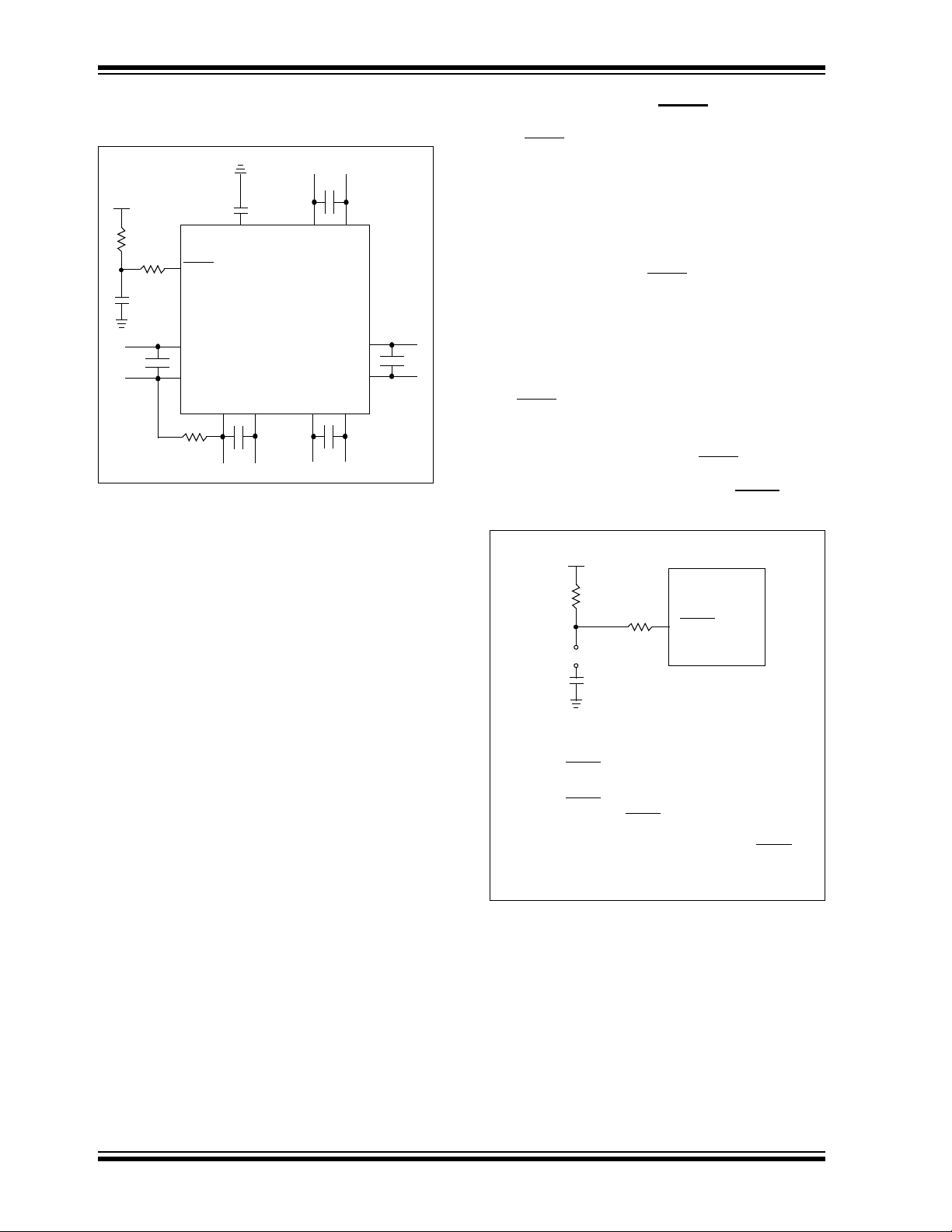
2.4 Master Clear (MCLR) Pin
The MCLR pin provides for two specific device
functions:
• Device Reset
• Device programming and debugging.
During device programming and debugging, the
resistance and capacitance that can be added to the
pin must be considered. Device programmers and
debuggers drive the MCLR
specific voltage levels (V
transitions must not be adversely affected. Therefore,
specific values of R and C will need to be adjusted
based on the application and PCB requirements.
For example, as shown in Figure 2-2, it is
recommended that the capacitor C, be isolated from
the MCLR
pin during programming and debugging
operations.
Place the components shown in Figure2-2 within
one-quarter inch (6mm) from the MCLR
FIGURE 2-2: EXAMPLE OF MCLR PIN
CONNECTIONS
pin. Consequently,
IH and VIL) and fast signal
pin.
2.3 Capacitor on Internal Voltage
Regulator (V
A low-ESR (< 5 Ohms) capacitor is required on the
CAP/VDDCORE pin, which is used to stabilize the
V
voltage regulator output voltage. The V
pin must not be connected to VDD, and must have a
capacitor bet ween 4.7µF and 10 µF, 16V connected to
ground. The type can be ceramic or tantalum. Refer to
Section 27.0 “Electrical Characteristics” for
additional information.
The placement of this capacitor should be close to the
CAP/VDDCORE. It is recommended that the trace
V
length not exceed one-quarter inch (6 mm). Refer to
Section 24.2 “On-Chip Voltage Regulator” for
details.
DS70591C-page 26 Preliminary 2010 Microchip Technology Inc.
CAP/VDDCORE)
CAP/VDDCORE
Page 27
dsPIC33FJ32GS406/606/608/610 and dsPIC33FJ64GS406/606/608/610
13
Main Oscillator
Guard Ring
Guard Trace
Secondary
Oscillator
14
15
16
17
18
19
20
2.5 ICSP Pins
The PGECx and PGEDx pins are used for In-Circuit
Serial Programming™ (ICSP™) and debugging purposes. It is recommended to keep the trace length
between the ICSP connec tor an d th e ICSP pi ns on th e
device as short as possible. If the ICSP connector is
expected to experience an ESD event, a serie s resistor
is recommended, with the value in the range of a few
tens of Ohms, not to exceed 100 Ohms.
Pull-up resistors, series diodes, and capacitors on the
PGCx and PGDx pins are not recommended as they
will interfere with the programmer/debugger communications to the device. If such discrete components are
an application requirement, they should be removed
from the circuit during programming and debugging.
Alternatively, refer to the AC/DC characteristics and
timing requirements information in the respective
device Flash programming specification for information
on capacitive loading limits and pin input voltage high
IH) and input low (VIL) requirements.
(V
Ensure that the “Communication Channel Select” (i.e.,
PGECx/PGEDx pins) programmed into the device
matches the physical connections for the ICSP to
MPLAB
ICE™.
For more information on ICD 2, ICD 3, and REAL ICE
connection requirements, refer to the following
documents that are available on the Microchip web
site.
• “MPLAB
• “Using MPLAB
• “MPLAB
• “Using MPLAB® ICD 3” (poster) DS51765
• “MPLAB® ICD 3 Design Advisory” DS51764
• “MPLAB
• “Using MPLAB
®
ICD 2, MPLAB® ICD 3, or MPLAB® REAL
®
ICD 2 In-Circuit Debugger User's
Guide” DS51331
®
®
®
ICD 2” (poster) DS51265
ICD 2 Design Advisory” DS51566
REAL ICE™ In-Circuit Debugger
User's Guide” DS51616
®
REAL ICE™” (poster) DS51749
2.6 External Oscillator Pins
Many DSCs have options for at least two oscillators: a
high-frequency primary oscillator and a low-frequency
secondary oscillator (refer to Section 9.0 “Oscillator
Configuration” for details).
The oscillator circuit should be placed on the same
side of the board as the device. Also, place the
oscillator circuit close to the respective oscillator pins,
not exceeding one-half inch (12 mm) distance
between them. The load capacitors should be placed
next to the oscillator itself, on the same side of the
board. Use a grounded copper pour around the
oscillator circuit to isolate them from surrounding
circuits. The grounded copper pour should be routed
directly to the MCU ground. Do not run any signal
traces or power traces inside the ground pour. Also, if
using a two-sided board, avoid any traces on the
other side of the board where the crystal is placed. A
suggested layout is shown in Figure 2-3.
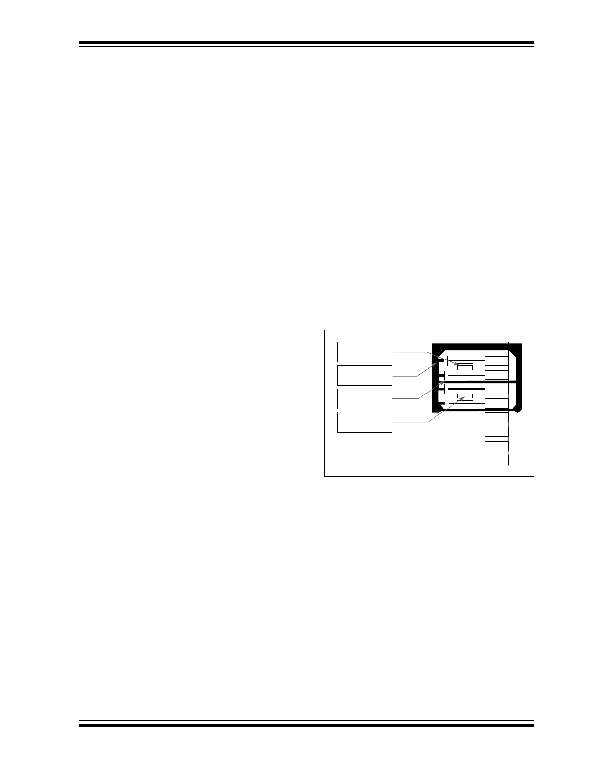
FIGURE 2-3: SUGGESTED PLACEMENT
OF THE OSCILLATOR
CIRCUIT
2010 Microchip Technology Inc. Preliminary DS70591C-page 27
Page 28

dsPIC33FJ32GS406/606/608/610 and dsPIC33FJ64GS406/606/608/610
2.7 Oscillator Value Conditions on
Device Start-up
If the PLL of the target device is enabled and
configured for the device start-up oscillator, the
maximum oscil lator source freque ncy must be limit ed
to 4 MHz < F
start-up conditions. This means that if the external
oscillator frequency is outside this range, the
application must start-up in the FRC mode first. The
default PLL settings after a POR with an oscillator
frequency outside this range will violate the device
operating speed.
Once the device powers up, the application firmware
can initialize the PLL SFR s, CLKDIV, and PLLDBF to a
suitable value, and then perform a clock switch to the
Oscillator + PLL clock source. Note that clock switching
must be enabled in the device Configuration Word.
IN < 8 MHz to comply with device PLL
2.8 Configuration of Analog and
Digital Pins During ICSP
Operations
If MPLAB ICD 2, ICD 3, or R EAL ICE i s sele cted as a
debugger, it automatical ly ini tia liz es al l of the A/D input
pins (ANx) as “digital” pins, by setting all bits in the
ADPCFG and ADPCFG2 registers.
The bits in the re gister s that co rrespond to the A/D pin s
that are initialized by MPLAB ICD 2, ICD 3, or REAL
ICE, must not be cleared by the user application
firmware; otherwise, communication errors will result
between the debugger and the device.
If your application needs to use certain A/D pins as
analog input pins during the debug session, the user
application must clear the corresponding bits in the
ADPCFG and ADPCFG2 registers during initialization
of the ADC module.
When MPLAB ICD 2, ICD 3, or REAL ICE is used as a
programmer, the user application firmware must
correctly configure the ADPCFG and ADPCFG2
registers. Automatic initialization of these registers is
only done during debugger operation. Failure to
correctly configure the register(s) will result in all A/D
pins being recogn ized as a nalog inpu t pins , res ulting in
the port value being read as a logic '0', which may
affect user application functionality.
2.9 Unused I/Os
Unused I/O pins s hould b e config ured as outputs and
driven to a logic-low state.
Alternatively, connect a 1k to 10k resistor to V
unused pins and drive the output to logic low.
SS on
2.10 Typical Application Connection
Examples
Examples of typical applicati on connecti ons are shown
in Figure 2-4 through Figure 2-11.
DS70591C-page 28 Preliminary 2010 Microchip Technology Inc.
Page 29
dsPIC33FJ32GS406/606/608/610 and dsPIC33FJ64GS406/606/608/610
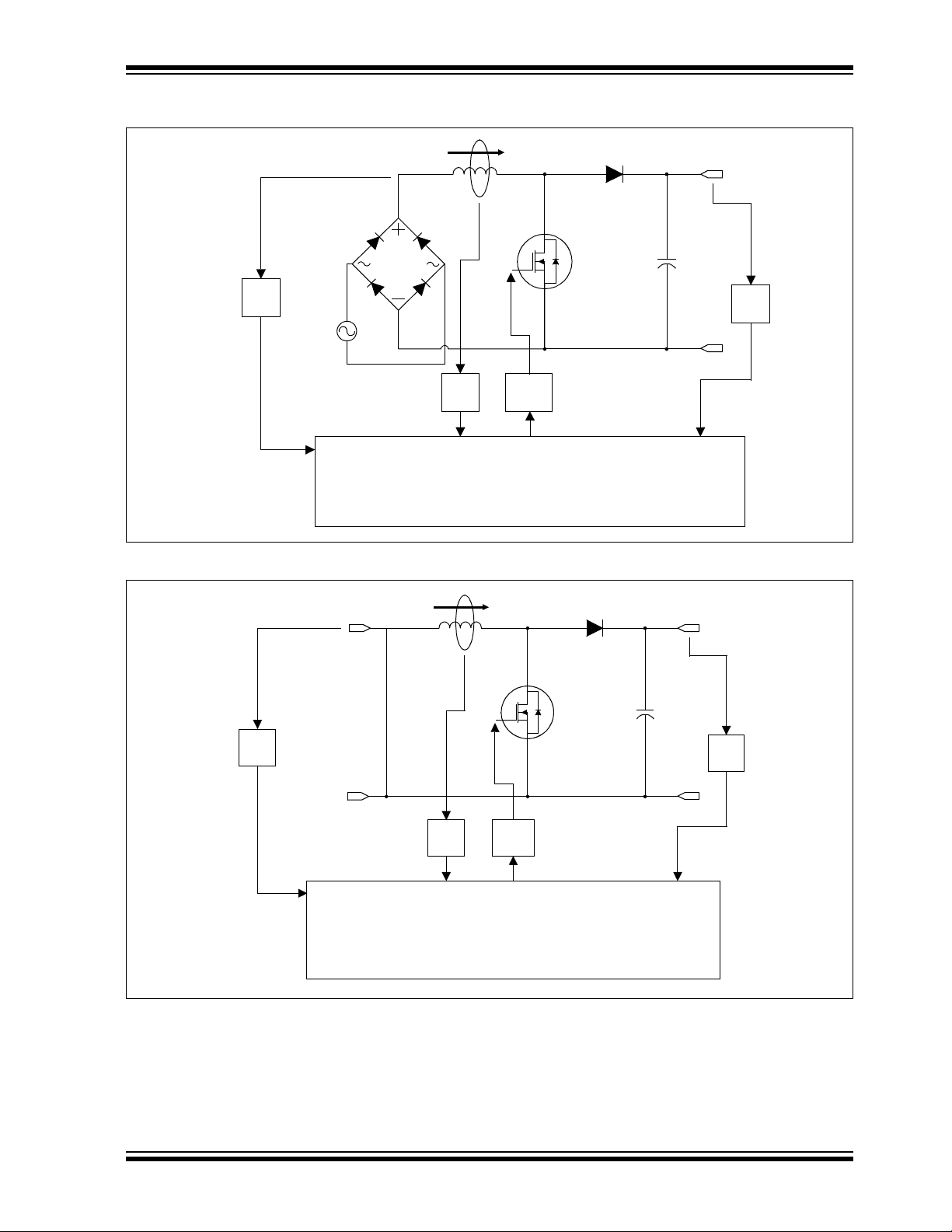
VAC
IPFC
VHV_BUS
ADC Channel
ADC Channel
ADC Channel
PWM Output
|V
AC|
k
1
k
2
k
3
FET
dsPIC33FJ32GS406
Driver
IPFC
VOUTPUT
ADC Channel
ADC
ADC Channel
PWM
k
1
k
2
k
3
FET
dsPIC33FJ32GS406
V
INPUT
Channel Output
Driver
FIGURE 2-4: DIGITAL PFC
FIGURE 2-5: BOOST CONVERTER IMPLEMENTATION
2010 Microchip Technology Inc. Preliminary DS70591C-page 29
Page 30
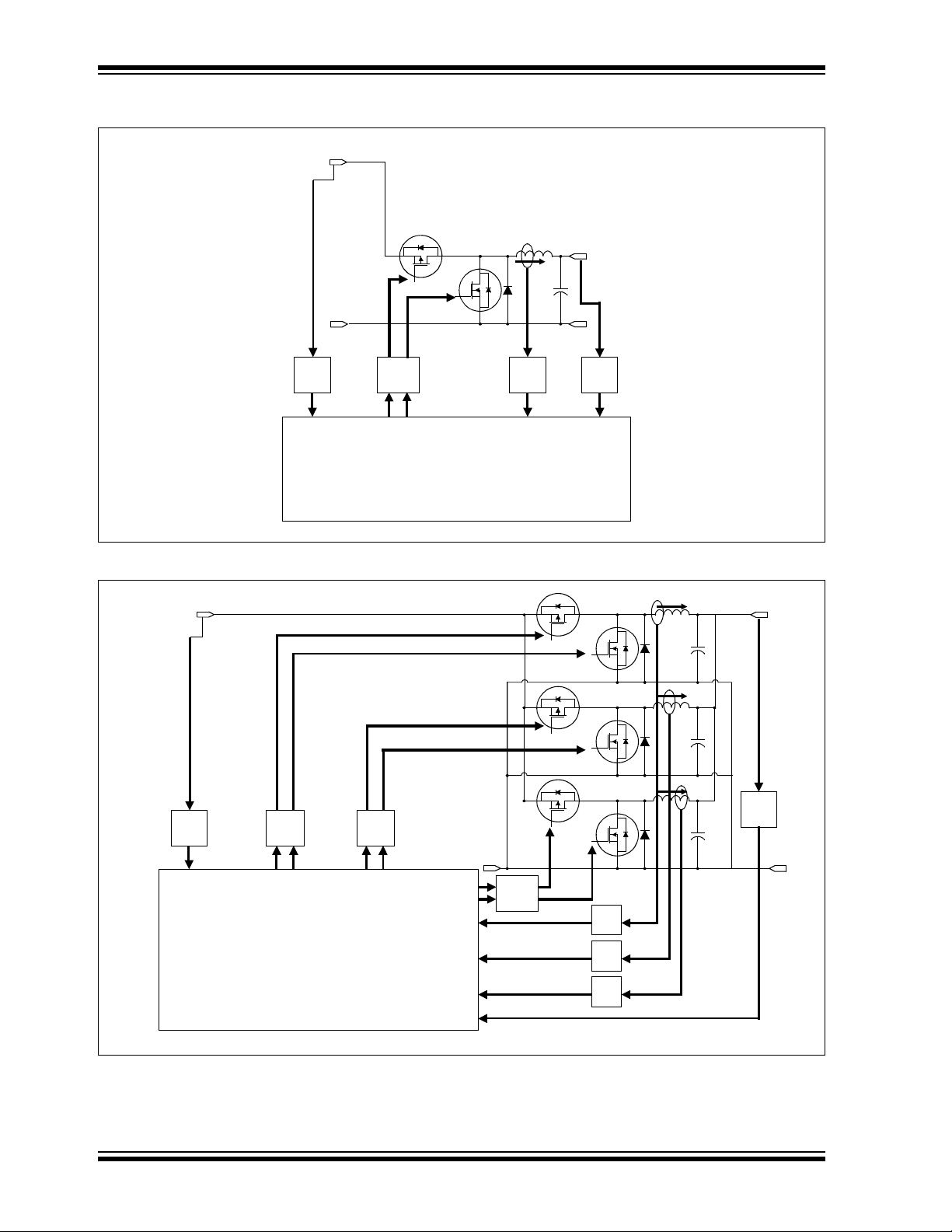
dsPIC33FJ32GS406/606/608/610 and dsPIC33FJ64GS406/606/608/610
k
1
Analog
Comp.
k
2
k
7
PWM
PWM
ADC
Channel
ADC
Channel
5V Output
I
5V
12V Input
FET
Driver
dsPIC33FJ32GS606
k
5
k
4
k
3
k
6
k
7
Analog Comparator
Analog Comparator
ADC Channel
Analog Comparator
ADC
Channel
PWM
PWM
PWM
PWM
PWM
PWM
3.3V Output
12V Input
FET
Driver
FET
Driver
FET
Driver
dsPIC33FJ32GS608
FIGURE 2-6: SINGLE-PHASE SYNCHRONOUS BUCK CONVERTER
FIGURE 2-7: MULTI-PHASE SYNCHRONOUS BUCK CONVERTER
DS70591C-page 30 Preliminary 2010 Microchip Technology Inc.
Page 31

dsPIC33FJ32GS406/606/608/610 and dsPIC33FJ64GS406/606/608/610
ADC
ADC
ADC
ADC
ADC
PWM PWMPWM
dsPIC33FJ64GS610
PWM PWM PWM
FET
Driver
FET
Driver
k
2
k
1
FET
Driver
FET
Driver
FET
Driver
FET
Driver
k
4
k
5
VBAT
GND
+
VOUT+
V
OUT-
Full-Bridge Inverter
Push-Pull Converter
V
DC
GND
FET
Driver
ADC
PWM
k
3
k
6
or
Analog Comp.
Battery Charger
+
FIGURE 2-8: OFF-LINE UPS
2010 Microchip Technology Inc. Preliminary DS70591C-page 31
Page 32

dsPIC33FJ32GS406/606/608/610 and dsPIC33FJ64GS406/606/608/610
VAC
VOUT+
ADC Channel
PWM
ADC
PWM
|V
AC|
k
4
k
3
FET
dsPIC33FJ32GS608
Driver
V
OUT-
ADC Channel
FET
Driver
ADC
k
1
k
2
Channel
Channel
ADC
Channel
FIGURE 2-9: INTERLEAVED PFC
DS70591C-page 32 Preliminary 2010 Microchip Technology Inc.
Page 33

dsPIC33FJ32GS406/606/608/610 and dsPIC33FJ64GS406/606/608/610
VIN+
V
IN-
S1
Gate 4
Gate 2
Gate 3
Gate 1
Analog
Ground
VOUT+
V
OUT-
dsPIC33FJ32GS606
PWM
PWM ADC
Channel
PWM ADC
Channel
k
2
FET
Driver
k
1
FET
Driver
FET
Driver
Gate 1
Gate 2
S1
Gate 3
Gate 4
S3
S3
Gate 6
Gate 5
Gate 6
Gate 5
FIGURE 2-10: PHA SE -SHIFTED FULL-BRIDGE CONVERTER
2010 Microchip Technology Inc. Preliminary DS70591C-page 33
Page 34

DS70591C-page 34 Preliminary 2010 Microchip Technology Inc.
k
4
ADC
Channel
PWM
UART
RX
PWM
PWM
IZVT
VHV_BUS
VOUT
Isolation
Barrier
ADC
Channel
PWM
PWM
PWM
FET
Driver
FET
Driver
FET
Driver
dsPIC33FJ64GS610
k
6
Analog
Comp.
UART
TX
k
10
k
7
k
9
k
8
k
11
k
5
PWM
PWM
ADC
Channel
Analog Comparator
Analog Comparator
ADC Channel
Analog Comparator
ADC
Channel
PWM
PWM
PWM
PWM
PWM
PWM
3.3V Output
5V Output
I
5V
12V Input
FET
Driver
FET
Driver
FET
Driver
FET
Driver
I
3.3V_3
I
3.3V_2
I
3.3V_1
dsPIC33FJ64GS610
VAC
IPFC
VHV_BUS
|VAC|
k
1
k
2
k
3
FET Driver
ADC
Ch.
ADC
Ch.
PWM
Output
ADC
Ch.
PFC Stage
3.3V Multi-Phase Buck Stage
ZVT with Current Doubler Synchronous Rectifier
5V Buck Stage
Secondary Controller
Primary Controller
FIGURE 2-11: AC-TO-DC POWER SUPPLY WITH PFC AND THREE OUTPUTS (12V, 5V, AND 3.3V)
dsPIC33FJ32GS406/606/608/610 and dsPIC33FJ64GS406/606/608/610
Page 35

dsPIC33FJ32GS406/606/608/610 and dsPIC33FJ64GS406/606/608/610
3.0 CPU
Note 1: This data sheet summarizes the features
of the dsPIC33FJ32GS406/606/608/610
and dsPIC33FJ64GS406/606/608/610
families of devi ces. It is not i ntended to be
a comprehensive reference source. To
complement the information in this data
sheet, refer to Section 2. “CPU”
(DS70204) in the “dsPIC33F/PIC24H
Family Reference Manual”, which is available from the Microchip web site
(www.microchip.com).
2: Some registers and associated bits
described in this section may not be available on all devices. Refer to Section 4.0
“Memory Organization” in this data
sheet for device-specific register and bit
information.
The dsPIC33FJ32GS406/606/608/610 and
dsPIC33FJ64GS406/606/608/610 CPU module has a
16-bit (data) modified Harvard architecture with an
enhanced instruction set, including significant support
for DSP. The CPU has a 24-bit instruction word with a
variable length opcode field. The Program Counter
(PC) is 23 bits wide and addresses up to 4M x 24 bits
of user program memory space. The actual amount of
program memory implemented varies from device to
device. A single-cycle instruction prefetch mechanism
is used to help maintain throughput and provides predictable execution. All instructions execute in a single
cycle, with the ex ception of i nstructions that change th e
program flow, the double-word move (MOV.D)
instruction and the table instructions. Overhead-free
program loop constructs are supported using the DO
and REPEAT instructions, both of which are
interruptible at any point.
The dsPIC33FJ32GS406/606/608/610 and
dsPIC33FJ64GS406/606/608/610 devices have sixteen, 16-bit working registers in the programmer’s
model. Each of the working registers can serve as a
data, address or address offset register. The sixteenth
working register (W15) operates as a software Stack
Pointer (SP) for interrupts and calls.
There are two classes of instruction in the
dsPIC33FJ32GS406/606/608/610 and
dsPIC33FJ64GS406/606/608/610 devices: MCU and
DSP. These two instruction classes are seamlessly
integrated into a single CPU. The instruction set
includes many addressing modes and is designed for
optimum C compiler eff iciency. For most instruct ions,
the dsPIC33FJ32GS406/606/608/610 and
dsPIC33FJ64GS406/606/608/610 is capable of executing a data (or program data) memory read, a working register (data) read, a data memory write and a
program (instruction) memory read per instruction
cycle. As a result, three parameter instructions can be
supported, allowing A + B = C operations to be
executed in a single cycle.
A block diagram of the CPU is shown in Figure 3-1,
and the programmer’s model for the
dsPIC33FJ32GS406/606/608/610 and
dsPIC33FJ64GS406/606/608/610 is shown in
Figure 3-2.
3.1 Data Addressing Overview
The data space can be addressed as 32K words or
64 Kbytes and is split into two blocks, referred to as X
and Y data memory. Each memory block has its own
independent Address Generation Unit (AGU). The
MCU class of instructions operates solely through
the X memory AGU, which accesses the entire
memory map as one linear data space. Certain DSP
instructions operate through the X and Y AGUs to
support dual operand reads, which splits the data
address space into two parts. The X and Y data space
boundary is device-specific.
Overhead-free circular buffers (Modulo Addressing
mode) are supported in both X and Y address spaces.
The Modulo Addressing removes the software
boundary checking overhead for DSP algorithms.
Furthermore, the X AGU circular addressing can be
used with any of the MCU class of instructions. The X
AGU also support s Bit-Rev ers ed Add r essin g to greatly
simplify input or output data reordering for radix-2 FFT
algorithms.
The upper 32 Kbytes of the data space memory map
can optionally be mapped into program space at any
16K program word boundary defined by the 8-bit
Program S pace Visibility Page (PSVPAG) register. The
program-to-data space mapping feature lets any
instruction access program space as if it were data
space.
3.2 DSP Engine Overview
The DSP engine features a high-speed, 17-bit by 17-bit
multiplier, a 40-bit ALU, two 40-bit saturating
accumulators and a 40-bit bidirectional barrel shifter.
The barrel shifter is c apable of shif ting a 40-bit value up
to 16 bits, right or left, in a single cycle. The DSP
instructions operate seamlessly with all other
instructions and have been designed for optimal realtime performance. The MAC i nstruc tion an d other a ssociated instructions can concurrently fetch two data
operands from memory while multiplying two W
registers and accumulating and optionally saturating
the result in the same cycle. This instruction
functionality requires that the RAM data space be split
for these instructions and linear for all others. Data
space partitioning is achieved in a transparent and
flexible manner through dedicating certain working
registers to each address space.
2010 Microchip Technology Inc. Preliminary DS70591C-page 35
Page 36

dsPIC33FJ32GS406/606/608/610 and dsPIC33FJ64GS406/606/608/610
Instruction
Decode &
Control
PCH PCL
Program Counter
16-Bit ALU
24
23
Instruction Reg
PCU
16 x 16
W Register Array
ROM Latch
EA MUX
Interrupt
Controller
Stack
Control
Logic
Loop
Control
Logic
Data Latch
Address
Latch
Control Signals
to Various Blocks
Literal Data
16
16
16
To Peripheral Modules
Data Latch
Address
Latch
16
X RAM
Y RAM
Address Generator Units
16
Y Data Bus
X Data Bus
DSP Engine
Divide Support
16
16
23
23
16
8
PSV & Table
Data Access
Control Block
16
16
16
16
Program Memory
Data Latch
Address Latch
3.3 Special MCU Features
The dsPIC33FJ32GS406/606/608/610 and
dsPIC33FJ64GS406/606/608/610 features a 17-bit by
17-bit single-cycl e multiplier that is shared by both the
MCU ALU and DSP engine. Th e multiplier can pe rform
signed, unsigned and mixed sign mult iplicatio n. Using a
17-bit by 17-bit multiplier for 16-bit by 16-bit multiplication
not only allows you to perf orm mixed sig n multip licati on,
it also achieves acc urate results for special operations,
such as (-1.0) x (-1.0 ).
The dsPIC33FJ32GS406/606/608/610 and
dsPIC33FJ64GS406/606/608/610 supports 16/16 and
32/16 divide operat ions, both fractional and intege r. All
divide instructions are iterative operations. They must be
executed within a REPEAT loop, resulting in a total
execution time of 19 instruction cycles. The divide
operation can be interrupted during any of those
19 cycles without loss of data.
A 40-bit barrel shifter is used to perform up to a 16-bit
left or right shift in a single cycle. The barrel shifter can
be used by both MCU and DSP instructions.
FIGURE 3-1: dsPIC33FJ32GS406/606/608/610 and dsPIC33FJ64GS406/606/608/610 CPU
CORE BLOCK DIAGRAM
DS70591C-page 36 Preliminary 2010 Microchip Technology Inc.
Page 37

dsPIC33FJ32GS406/606/608/610 and dsPIC33FJ64GS406/606/608/610
PC22
PC0
7
0
D0D15
Program Counter
Data Table Page Address
STATUS Register
Working Registers
DSP Operand
Registers
W1
W2
W3
W4
W5
W6
W7
W8
W9
W10
W11
W12/DSP Offset
W13/DSP Write Back
W14/Frame Pointer
W15/Stack Pointer
DSP Address
Registers
AD39 AD0AD31
DSP
Accumulators
ACCA
ACCB
7
0
Program Space Visibility Page Address
Z
0
OA OB SA SB
RCOUNT
15
0
REPEAT Loop Counter
DCOUNT
15
0
DO Loop Counter
DOSTART
22
0
DO Loop Start Address
IPL2 IPL1
SPLIM
Stack Pointer Limit Register
AD15
SRL
PUSH.S Shadow
DO Shadow
OAB SAB
15
0
Core Configuration Register
Legend
CORCON
DA DC
RA N
TBLPAG
PSVPAG
IPL0 OV
W0/WREG
SRH
DO Loop End Address
DOEND
22
C
FIGURE 3-2: PROGRAMMER’S MODEL
2010 Microchip Technology Inc. Preliminary DS70591C-page 37
Page 38

dsPIC33FJ32GS406/606/608/610 and dsPIC33FJ64GS406/606/608/610
3.4 CPU Control Registers
REGISTER 3-1: SR: CPU STATUS REGISTER
R-0 R-0 R/C-0 R/C-0 R-0 R/C-0 R -0 R/W-0
OA OB SA
(1)
bit 15 bit 8
SB
(1)
OAB SAB
(1,4)
DA DC
R/W-0
(2)
IPL<2:0>
R/W-0
(3)
(2)
R/W-0
(3)
R-0 R/W-0 R/W-0 R/W-0 R/W-0
RA N OV Z C
bit 7 bit 0
Legend:
C = Clearable bit R = Readable bit U = Unimplemented bit, read as ‘0’
S = Settable bit W = Writable bit -n = Value at POR
‘1’ = Bit is set ‘0’ = Bit is cleared x = Bit is unknown
bit 15 OA: Accumulator A Overflow Status bit
1 = Accumul ator A overflowed
0 = Accumulator A has not overflowed
bit 14 OB: Accumulator B Overflow Status bit
1 = Accumul ator B overflowed
0 = Accumulator B has not overflowed
bit 13 SA: Accumulator A Saturation ‘Sticky’ Status bit
(1)
1 = Accumulator A is saturated or has been saturated at some time
0 = Accumulator A is not satura ted
bit 12 SB: Accumulator B Saturation ‘Sticky’ Status bit
(1)
1 = Accumulator B is saturated or has been saturated at some time
0 = Accumulator B is not satura ted
bit 11 OAB: OA || OB Combined Accumulator Overflow Status bit
1 = Accumulators A or B have overflowed
0 = Neither Accumulators A or B have overflowed
bit 10 SAB: SA || SB Combined Accumulator ‘Sticky’ Status bit
(1,4)
1 = Accumulators A or B are saturated or have been saturated at some time in the past
0 = Neither Accumulator A or B are saturated
bit 9 DA: DO Loop Active bit
1 = DO loop in progress
0 = DO loop not in progress
bit 8 DC: MCU ALU Half Carry/Borrow bit
1 = A carry-out from the 4th low-order bit (for byte-sized dat a) or 8th low-orde r bit (for word-sized dat a)
of the result occurred
0 = No carry-out from the 4th low-order bit (for byte-sized data) or 8th low-order bit (for word-sized
data) of the result occurred
Note 1: This bit can be read or cleared (not set).
2: The IPL<2:0> bits are conca ten ated with the IPL<3 > bi t (CO RCON<3>) to form the CPU Inte rrup t Prio rity
Level (IPL ). Th e val ue i n pare nth ese s ind ica tes t he I PL i f IPL <3> = 1. User interrupts are disabled when
IPL<3> = 1.
3: The IPL<2:0> Sta tus bit s are read -on ly w hen NSTDIS = 1 (INTCON1<15>).
4: Clearing this bit will clear SA and SB.
DS70591C-page 38 Preliminary 2010 Microchip Technology Inc.
Page 39

dsPIC33FJ32GS406/606/608/610 and dsPIC33FJ64GS406/606/608/610
REGISTER 3-1: SR: CPU STATUS REGISTER (CONTINUED)
bit 7-5 IPL<2:0>: CPU Interrupt Priority Level Status bits
111 = CPU Interrupt Priority Level is 7 (15), user interrupts disabled
110 = CPU Interrupt Priority Level is 6 (14)
101 = CPU Interrupt Priority Level is 5 (13)
100 = CPU Interrupt Priority Level is 4 (12)
011 = CPU Interrupt Priority Level is 3 (11)
010 = CPU Interrupt Priority Level is 2 (10)
001 = CPU Interrupt Priority Level is 1 (9)
000 = CPU Interrupt Priority Level is 0 (8)
bit 4 RA: REPEAT Loop Active bit
1 = REPEAT loop in prog ress
0 = REPEAT loop not in pr ogress
bit 3 N: MCU ALU Negative bit
1 = Result was negative
0 = Result was non-negative (zero or positive)
bit 2 OV: MCU ALU Overflow bit
This bit is used for signed arithmetic (2’s complement). It indicates an overflow of a magnitude that
causes the sign bit to change state.
1 = Overflow occurred for signed arithmetic (in this arithmetic operation)
0 = No overflow occurred
bit 1 Z: MCU ALU Zero bit
1 = An operation that affects the Z bit has set it at some time in the past
0 = The most recent operation that affects the Z bit has cleared it (i.e., a non-zero result)
bit 0 C: MCU ALU Carry/Borrow
1 = A carry-out from the Most Significant bit of the result occurred
0 = No carry-out from the Most Significant bit of the result occurred
bit
(2)
Note 1: This bit can be read or cleared (not set).
2: The IPL<2:0> bits are conca ten ated with the IPL<3 > bi t (CO RCON<3>) to form the CPU Inte rrup t Prio rity
Level (IPL ). Th e val ue i n pare nth ese s ind ica tes t he I PL i f IPL <3> = 1. User interrupts are disabled when
IPL<3> = 1.
3: The IPL<2:0> Sta tus bit s are read -on ly w hen NSTDIS = 1 (INTCON1<15>).
4: Clearing this bit will clear SA and SB.
2010 Microchip Technology Inc. Preliminary DS70591C-page 39
Page 40

dsPIC33FJ32GS406/606/608/610 and dsPIC33FJ64GS406/606/608/610
REGISTER 3-2: CORCON: CORE CONTROL REGISTER
U-0 U-0 U-0 R/W-0 R/W-0 R-0 R-0 R-0
— — —USEDT
(1)
DL<2:0>
bit 15 bit 8
R/W-0 R/W-0 R/W-1 R/W-0 R/C-0 R/W-0 R/W-0 R/W-0
SATA SATB SATDW ACCSAT IPL3
(2)
PSV RND IF
bit 7 bit 0
Legend: C = Clearable bit
R = Readable bit W = Writable bit -n = Value at POR ‘1’ = Bit is set
0’ = Bit is cleared ‘x = Bit is unknown U = Unimplemented bit, read as ‘0’
bit 15-13 Unimplemented: Read as ‘0’
bit 12 US: DSP Multiply Unsigned/Signed Control bit
1 = DSP engine multiplies are unsigned
0 = DSP engine multiplies are signed
bit 11 EDT: Early DO Loop Termination Control bit
(1)
1 = Terminate executing DO loop at end of current loop iteration
0 = No effect
bit 10-8 DL<2:0>: DO Loop Nesting Level Status bits
111 = 7 DO loops active
•
•
•
001 = 1 DO loop active
000 = 0 DO loops active
bit 7 SATA: ACCA Saturation Enable bit
1 = Accumulator A saturation enabled
0 = Accumulator A saturation disabled
bit 6 SATB: ACCB Saturation Enable bit
1 = Accumulator B saturation enabled
0 = Accumulator B saturation disabled
bit 5 SATDW: Data Space Write from DSP Engine Saturation Enable bit
1 = Data space write saturation enabled
0 = Data space write saturation disabled
bit 4 ACCSAT: Accumulator Saturation Mode Select bit
1 = 9.31 saturation (super saturation)
0 = 1.31 saturation (normal saturation)
bit 3 IPL3: CPU Interrupt Priority Level Status bit 3
(2)
1 = CPU Interrupt Priority Level is greater than 7
0 = CPU Interrupt Priority Level is 7 or less
bit 2 PSV: Program Space Visibility in Data Space Enable bit
1 = Program space visible in data space
0 = Program space not visible in data space
bit 1 RND: Rounding Mode Select bit
1 = Biased (conventional) rounding enabled
0 = Unbiased (convergent) rounding enabled
bit 0 IF: Integer or Fractional Multiplier Mode Select bit
1 = Integer mode enabled for DSP multiply ops
0 = Fractional mode enabled for DSP multiply ops
Note 1: This bit will always read as ‘0’.
2: The IPL3 bit is concatenated with the IPL<2:0> bits (SR<7:5>) to form the CPU Interrupt Priority Level.
DS70591C-page 40 Preliminary 2010 Microchip Technology Inc.
Page 41

dsPIC33FJ32GS406/606/608/610 and dsPIC33FJ64GS406/606/608/610
3.5 Arithmetic Logic Unit (ALU)
The dsPIC33FJ32GS406/606/608/610 and
dsPIC33FJ64GS406/606/608/610 ALU is 16 bits wide
and is capable of addition, subtraction, bit shifts and logic
operations. Unless otherwise mentioned, arithmetic
operations are 2’s complemen t in nat ure. D epending on
the operation, the ALU can affect the values of the Carry
(C), Zero (Z), Negat ive (N), Overflow (OV) an d Digit Carry
(DC) Status bits in the SR register. The C and DC Status
bits operate as Borrow
for subtra c ti o n op e r a ti o ns .
The ALU can perform 8-bit or 16-bit operations,
depending on the mode of the instruction that is used.
Data for the ALU operation can come from the W
register array or data memory, depending on the
addressing mode of the instruction. Likewise, output
data from the ALU ca n be written to the W re gister array
or a data memory location.
Refer to the “16-bit MCU and DSC Programmer’s Ref-
erence Manual” (DS70157) for information on the SR
bits affected by each instruction.
The dsPIC33FJ32GS406/606/608/610 and
dsPIC33FJ64GS406/606/608/610 CPU incorporates
hardware support for both multiplication and division. This
includes a dedicated hardware multiplier and support
hardware for 16-bit-divisor division.
3.5.1 MULTIPLIER
Using the high-speed, 17-bit x 17-bit multiplier of the
DSP engine, the ALU supports unsigned, signed or
mixed sign operation in several MCU multiplication
modes:
• 16-bit x 16-bit signed
• 16-bit x 16-bit unsigned
• 16-bit signed x 5-bit (literal) unsigned
• 16-bit unsigned x 16-bit unsigned
• 16-bit unsigned x 5-bit (literal) unsigned
• 16-bit unsigned x 16-bit signed
• 8-bit unsigned x 8-bit unsigned
and Digit Borrow bits, respectively,
3.5.2 DIVIDER
The divide block support s 32-bit/16-bit and 16-b it/16-bit
signed and unsig ne d in teg er d iv ide ope rati ons with the
following data sizes:
• 32-bit signed/16-bit signed divide
• 32-bit unsigned/16-bit unsigned divide
• 16-bit signed/16-bit signed divide
• 16-bit unsigned/16-bit unsigned divide
The quotient fo r all divid e instru ctions ends up in W0 and
the remainder in W1. 16-bit signed and unsigned DIV
instructions can specify an y W register for bo th the 16-bit
divisor (Wn) and any W register (aligned) pair
(W(m + 1):Wm) for the 32-bit dividend. The divide
algorithm t akes one cycl e per bit of divisor , so bo th 32-bit/
16-bit and 16-bit/16-bit instructions take the same
number of cycles to execute.
3.6 DSP Engine
The DSP engine consists of a high-speed, 17-bit x
17-bit multiplier, a barrel shifter and a 40-bit adder/
subtracter (with two target accumulators, round and
saturation logic).
The dsPIC33FJ32GS406/606/608/610 and
dsPIC33FJ64GS406/606/608/610 is a single-cycle
instruction flow architecture; therefore, concurrent operation of the DSP engine wi th MCU instruction f low is not
possible. However, some MCU ALU and DSP engine
resources can be used concurrently by the same instruction (for example, ED, EDAC).
The DSP engine can also perform inherent
accumulator-to-accu mu lator operations that require no
additional data. These instructions are ADD, SUB and
NEG.
The DSP engine has options selected through bits in
the CPU Core Control register (CORCON), as listed
below:
• Fractional or integer DSP multiply (IF)
• Signed or unsigned DSP multiply (US)
• Conventional or convergent rounding (RND)
• Automatic saturation on/off for ACCA (SATA)
• Automatic saturation on/off for ACCB (SATB)
• Automatic saturation on/off for writes to data
memory (SATDW)
• Accumulator Saturation mode selection (ACCSAT)
A block diagram of the DSP engine is shown in
Figure 3-3.
2010 Microchip Technology Inc. Preliminary DS70591C-page 41
Page 42

dsPIC33FJ32GS406/606/608/610 and dsPIC33FJ64GS406/606/608/610
Zero Backfill
Sign-Extend
Barrel
Shifter
40-bit Accumulator A
40-bit Accumulator B
Round
Logic
X Data Bus
To/From W Array
Adder
Saturate
Negate
32
32
33
16
16
16
16
40
40
40
40
S
a
t
u
r
a
t
e
Y Data Bus
40
Carry/Borrow Out
Carry/Borrow In
16
40
Multiplier/Scaler
17-Bit
TABLE 3-1: DSP INSTRUCTIONS SUMMARY
Instruction Algebraic Operation ACC Write Back
CLR A = 0
ED A = (x – y)2 No
EDAC A = A + (x – y)2 No
MAC A = A + (x * y) Yes
MAC A = A + x2 No
MOVSAC No change in A Yes
MPY A = x * y No
MPY A = x 2 No
MPY.N A = – x * y No
MSC A = A – x * y Yes
FIGURE 3-3: DSP ENGINE BLOCK DIAGRAM
Yes
DS70591C-page 42 Preliminary 2010 Microchip Technology Inc.
Page 43

dsPIC33FJ32GS406/606/608/610 and dsPIC33FJ64GS406/606/608/610
3.6.1 MULTIPLIER
The 17-bit x 17-bit multiplier is capable of signed or
unsigned operati on and can mul tiplex i ts ou tput u sing a
scaler to support either 1.31 fractional (Q31) or 32-bit
integer results. Unsigned operands are zero-extended
into the 17th bit of the multiplier input value. Signed
operands are sign-extended into the 17th bit of the
multiplier input value. The output of the 17-bit x 17-bit
multiplier/ scale r is a 33-bit valu e that i s sign -ext ended
to 40 bits. Integer data is inherently represented as a
signed 2’s complement value, where the Most
Significant bit (MSb) is defined as a sign bit. Th e range
of an N-bit 2’s complement integer is -2
• For a 16-bit integer, the data range is -32768
(0x8000) to 32767 (0x7FFF) including 0.
• For a 32-bit integer, the data range is
-2,147,483,648 (0x80000000) to 2,147,483,647
(0x7FFF FFFF).
When the multiplier is configured for fractional
multiplication, the data is represented as a 2’s
complement fraction, where the MSb is defined as a
sign bit and the radix po int is impli ed to lie just af ter the
sign bit (QX format). The range of an N-bit 2’s
complement fract ion with this im plie d radix point i s -1.0
to (1 – 2
is -1.0 (0x8000) to 0.999969482 (0x7FFF) including 0
and has a precision of 3.01518x10⁻⁵. In Fractional
mode, the 16 x 16 multiply operation generates a
1.31 product that has a precision of 4.65661 x 10
The same multiplier is used to support the MCU
multiply instructions, which include integer 16-bit
signed, unsigned and mixed sign multiply operations.
The MUL instruction can be directed to use byte or
word-sized operands. Byt e operan ds will direct a 16-bit
result, and word operands will direct a 32-bit result to
the specified register(s) in the W array.
1-N
). For a 16-bit fraction, the Q15 data range
N-1
to 2
N-1
– 1.
-10
.
3.6.2 DATA ACCUMULATORS AND
ADDER/SUBTRACTER
The data accumulator consists of a 40-bit adder/
subtracter with automatic sign extension logic. It can
select one of two accumulators (A or B) as its preaccumulation source and post-accumulation
destination. For t he ADD and LAC instructions, the da t a
to be accumulated or loaded can be optionally scaled
using the barrel shifter prior to accumulation.
3.6.2.1 Adder/Subtracter, Overflow and
Saturation
The adder/subtracter is a 40-bit adder with an optional
zero input into one si de, and either true or comp leme nt
data into the other input.
• In the case of addition, the Carry/B
active-high and the other input is true data (not
complemented).
• In the case of subtraction, the Carry/Borrow input
is active-low and the ot her inpu t is comple mente d.
The adder/subtracter generates Overflow Status bits,
SA/SB and OA/OB, which are latched and reflected in
the STATUS register:
• Overflow from bit 39: this is a catastrophic
overflow in which the sign of the accumulator is
destroyed.
• Overflow into guard bits, 32 through 39: this is a
recoverable overflow. This bit is set whenever all
the guard bits are not identical to each other.
The adder has an additional saturation block that
controls accumulator data saturation, if selected. It
uses the result of the adder, the Overflow Status bits
described previously and the SAT<A:B>
(CORCON<7:6>) and ACCSAT (CORCON<4>) mode
control bits to determine when and to what value to
saturate.
Six STATUS register bits support saturation and
overflow:
• OA: ACCA overflowed into guard bits
• OB: ACCB overflowed into guard bits
• SA: ACCA saturated (bit 31 overflow and
saturation)
or
ACCA overflowed into guard bits and saturated
(bit 39 overflow and saturation)
• SB: ACCB saturated (bit 31 overflow and
saturation)
or
ACCB overflowed into guard bits and saturated
(bit 39 overflow and saturation)
• OAB: Logical OR of OA and OB
• SAB: Logical OR of SA and SB
The OA and OB bits are modified each time data
passes through the adder/subtracter. When set, they
indicate that the most recent operation has overflowed
into the accumulator guard bits (bits 32 through 39).
The OA and OB bits can also optionally generate an
arithmetic warning trap when set and the corresponding Overflow Trap Flag Enable bits (OVATE, OVBTE)
in the INTCON1 register are set (refer to Section 7.0
“Interrupt Controller”). This allows the us er applica tion to take immediate action, for example, to correct
system gain.
orrow input is
2010 Microchip Technology Inc. Preliminary DS70591C- page 43
Page 44

dsPIC33FJ32GS406/606/608/610 and dsPIC33FJ64GS406/606/608/610
The SA and SB bits are modified each time data
passes through the adder/subtracter, but can only be
cleared by the u ser applic ation. When set, they indicate
that the accumulator has overflowed its maximum
range (bit 31 for 32-bit saturation or bit 39 for 40-bit
saturation) and will be saturated (if saturation is
enabled). When saturation is not enabled, SA and SB
default to bit 39 overflow and thus, indic ate that a ca tastrophic overflow has o cc urred . If th e CO VTE bi t in th e
INTCON1 register is set, SA and SB bits will generate
an arithmetic warning trap when saturation is disabled.
The Overfl ow and Saturation Status bits c an optionally
be viewed in the STATUS Register (SR) as the logical
OR of OA and OB (in bit OAB) and the logical OR of SA
and SB (in bit SAB). Programmers can check one bit in
the ST ATUS register to determine if either ac cumula tor
has overflowed, or one bit to determine if either
accumulator has saturated. This is useful for complex
number arithmetic, which typically uses both
accumulators.
The device supports three Saturation and Overflow
modes:
• Bit 39 Overflow and Saturation:
When bit 39 overflow and saturation occurs, the
saturation logic loads the maximally positive
9.31 (0x7FFFFFFFFF) or maximally negative
9.31 value (0x8000000000) into the target accumulator. The SA or SB bit is set and remains set un til
cleared by the user application. This condition is
referred to as ‘super saturation’ and provides
protection against erroneous data or unexpected
algorithm problems (such as gain calculations).
• Bit 31 Overflow and Saturation:
When bit 31 overflow and saturation occurs, the
saturation logic then loads the maximally positive
1.31 value (0x007FFFFFFF) or maximally negative 1.31 value (0x0080000000) into the target
accumulator. The SA or SB bit is set and remains
set until cleared by the user application. When
this Saturation mode is in effect , the guard bit s are
not used, so the OA, OB or OAB bits are never
set.
• Bit 39 Catastrophic Overflow:
The bit 39 Overflow Status bit from the adder is
used to set the SA or SB bit, which remains set
until cleared by the user applic ation. No sa turation
operation is performed, and the accumulator is
allowed to overflow, destroying its sign. If the
COVTE bit in the INTCON1 register is set, a
catastrophic ov erfl ow ca n i nitiate a trap excep tio n.
3.6.3 ACCUMULATOR ‘WRITE BACK’
The MAC class of instructions (with the exception of
MPY, MPY.N, ED and EDAC) can optionally write a
rounded ver sion of the hi gh word (bits 31 t hroug h 16)
of the accumulator tha t is not targeted by the instructio n
into data spac e memory. The write is performed across
the X bus into combined X and Y address space. The
following addressing modes are supported:
• W13, Register Direct:
The rounded contents of the non-target
accumulator are written into W13 as a
1.15 fraction.
• [W13] + = 2, Register Indirect with Post-Increment:
The rounded contents of the non-target
accumulator are writte n into the addr ess pointed
to by W13 as a 1.15 fraction. W13 is then
incremented by 2 (for a word write).
3.6.3.1 Round Logic
The round logic is a combinational block that performs
a conventional (biased) or convergent (unbiased)
round function durin g an ac cumulat or write (store). Th e
Round mode is determined by the state of the RND bit
in the CORCON register. It generates a 16-bit,
1.15 data value that is passed to the data space write
saturation logic. If rounding is not indicated by the
instruction, a truncated 1.15 data value is stored and
the least significant word is simply discarded.
Conventional roundi ng zero-exten ds bit 15 of t he accumulator and adds it to the A CCxH word (bits 1 6 through
31 of the accumulator).
• If the ACCxL word (bits 0 through 15 of the
accumulator) is between 0x8000 and 0xFFFF
(0x8000 included), ACCxH is incremented.
• If ACCxL is between 0x0 000 and 0x 7FFF, ACCxH
is left unchanged.
A consequence of this algorithm is that over a
succession of random rounding operations, the value
tends to be biased slightly positive.
Convergent (or unbiased) rounding operates in the
same manner as conventional rounding, except when
ACCxL equals 0x8000. In this case, the Least
Significant bit (bit 16 of the accumulator) of ACCxH is
examined:
• If it is ‘1’, ACCxH is incremented.
• If it is ‘0’, ACCxH is not modified.
Assuming that bit 16 is effectively random in nature,
this scheme removes any rounding bias that may
accumulate.
The SAC and SAC.R instructions store either a
truncated (SAC), or rounded (SAC.R) version of the
contents of the target accumulator to data memory via
the X bus, subject to data saturation (see
Section 3.6.3.2 “Data Space Write Saturation”). For
the MAC class of instructions, the accumulator writeback operation functions in the same manner,
addressing combined MCU (X and Y) data space
though the X bus. For this class of instruc tions, the data
is always subject to rounding.
DS70591C-page 44 Preliminary 2010 Microchip Technology Inc.
Page 45

dsPIC33FJ32GS406/606/608/610 and dsPIC33FJ64GS406/606/608/610
3.6.3.2 Data Space Write Saturation
In addition to adder/subtrac ter saturation, writes to dat a
space can also be saturated, but without affecting the
contents of the source accumulator. The data space
write saturation logic block accepts a 16-bit, 1.15
fractional value from the round logic block as its input,
together with overflow status from the original source
(accumulator) and the 1 6-bit round adde r . These in puts
are combined and used to select the appropriate
1.15 fractional value as output to write to data space
memory.
If the SATDW bit in the CORCON register is set, data
(after rounding or truncat ion ) is tested for overflow and
adjusted accordingly:
• For input data greater than 0x007FFF, data
written to memory is forced to the maximum
positive 1.15 value, 0x 7FFF.
• For input dat a les s tha n 0x FF8000, dat a w ritten to
memory is forced to the maximum negative
1.15 value, 0x8000.
The Most Significan t bit of the source (bit 39) is used to
determine the sign of the operand being tested.
If the SA TDW bi t in the CORCON regis ter is not set , the
input data is always passed through unmodified under
all conditions.
3.6.4 BARREL SHIFTER
The barrel shifter ca n perform up to 1 6-bit arithme tic or
logic right shifts, or up to 16-bit left shifts in a single
cycle. The source can be either of the two DSP
accumulators or the X bus (to su pport multi-bit shif t s of
register or memory data).
The shifter requires a signed binary value to determine
both the magnitude (num ber of bits) and direction of the
shift operation. A positive value shif ts the operand right.
A negative v alue shi fts the opera nd left. A va lue of ‘ 0’
does not modify the operand.
The barrel shifter is 40 bits wide, thereby obtaining a
40-bit result fo r DSP shif t o peratio ns a nd a 16-bit re sult
for MCU shift operations. Data from the X bus is
presented to the barrel shifter between bit positions 16
and 31 for right shifts, and between bit positions 0 and
16 for left shifts.
2010 Microchip Technology Inc. Preliminary DS70591C- page 45
Page 46

dsPIC33FJ32GS406/606/608/610 and dsPIC33FJ64GS406/606/608/610
NOTES:
DS70591C-page 46 Preliminary 2010 Microchip Technology Inc.
Page 47

dsPIC33FJ32GS406/606/608/610 and dsPIC33FJ64GS406/606/608/610
Reset Address
0x000000
0x0000FE
0x000002
0x000100
Device Configuration
User Program
Flash Memory
0x005800
0x0057FE
(11008 instructions)
0x800000
0xF80000
Registers
0xF80017
0xF80018
DEVID (2)
0xFEFFFE
0xFF0000
0xFFFFFE
0xF7FFFE
Unimplemented
(Read ‘0’s)
GOTO Instruction
0x000004
Reserved
0x7FFFFE
Reserved
0x000200
0x0001FE
0x000104
Alternate Vector Table
Reserved
Interrupt Vector Table
dsPIC33FJ32GS406/606/608/610
Configuration Memory Space
User Memory Space
Reset Address
0x000000
0x0000FE
0x000002
0x000100
Device Configuration
User Program
Flash Memory
0x00AC00
0x00ABFE
(21760 instructions)
0x800000
0xF80000
Registers
0xF80017
0xF80018
0xF7FFFE
Unimplemented
(Read ‘0’s)
GOTO Instruction
0x000004
Reserved
0x7FFFFE
Reserved
0x000200
0x0001FE
0x000104
Alternate Vector Table
Reserved
Interrupt Vector Table
dsPIC33FJ64GS406/606/608/610
Configuration Memory Space
User Memory Space
Reserved
0xFF0002
DEVID (2)
Reserved
0xFEFFFE
0xFF0000
0xFFFFFE
0xFF0002
4.0 MEMORY ORGANIZATION
Note: This data sheet summarizes the features
of the dsPIC33FJ32GS406/606/608/610
and dsPIC33FJ64GS406/606/608/610
families of devices. It is not intended to be
a comprehensive reference source. To
complement the information in this data
sheet, refer to the dsPIC33F/PIC24H
Family Reference Manual, “Section 4.
Program Memory” (DS70202), which is
available from the Microchip web site
(www.microchip.com).
4.1 Program Address Space
The program address memory space of the
dsPIC33FJ32GS406/606/608/610 and
dsPIC33FJ64GS406/606/608/610 devices is 4M
instructions. The space is addressable by a 24-bit
value deriv ed either from t he 23-bit Progr am Counter
(PC) during program execution, or from table operation
or data space remapp ing as des cribed in Section 4.6
“Interfacing Program and Data Memory Spaces”.
User application acc ess to the program me mory sp ac e
is restricted to the lower half of the address range
(0x000000 to 0x7FFFFF). The exception is the use of
TBLRD/TBLWT operations, which use TBLPAG<7> to
The dsPIC33FJ32GS406/606/608/610 and
dsPIC33FJ64GS406/606/608/610 architecture features
separate program and data memor y spaces a nd buses.
This architecture also allows the direct access to program
memory from the data space during code execution.
permit access to the Configuration bits and Device ID
sections of the configuration memory space.
The memory maps for the
dsPIC33FJ32GS406/606/608/610 and
dsPIC33FJ64GS406/606/608/610 devices are shown
in Figure 4-1.
FIGURE 4-1: PROGRAM MEMORY MAPS FOR dsPIC33FJ32GS406/606/608/610 and
dsPIC33FJ64GS406/606/608/610 DEVICES
2010 Microchip Technology Inc. Preliminary DS70591C- page 47
Page 48

dsPIC33FJ32GS406/606/608/610 and dsPIC33FJ64GS406/606/608/610
0816
PC Address
0x000000
0x000002
0x000004
0x000006
23
00000000
00000000
00000000
00000000
Program Memor y
‘Phantom’ Byte
(read as ‘0’)
least signi ficant word
most significant word
Instruction Width
0x000001
0x000003
0x000005
0x000007
msw
Address (lsw Address)
4.1.1 PROGRAM MEMORY
ORGANIZATION
The program memory space is organized in
word-addressable blocks. Although it is treated as
24 bits wide, it is more appropriate to think of each
address of the program memory as a lower and upper
word, with the upper byte of the upper word being
unimplemented. The lower word always has an even
address, while the upper word has an od d address (see
Figure 4-2).
Program memory addresses are always word-aligned
on the lower word, and addresses are incremented or
decremented by two during the code execution. This
arrangement provides compatibility with data memory
space addressing and makes data in the program
memory space accessible.
4.1.2 INTERRUPT AND TRAP VECTORS
All dsPIC33FJ32GS406/606/608/610 and
dsPIC33FJ64GS406/606/608/610 devices reserve the
addresses between 0x00000 and 0x000200 for
hard-coded program execution vectors. A hardware
Reset vector is provided to redire ct code executi on from
the default value of the PC on device Reset to the actual
start of code. A GOTO instruction is programmed by the
user application at 0x000000, with the actual address for
the start of code at 0x000002.
The dsPIC33FJ32GS406/606/608/610 and
dsPIC33FJ64GS406/606/608/610 devices also have
two interr upt vector tables , located from 0x000004 to
0x0000FF and 0x000100 to 0x0001FF. These vector
tables allow each of the device interrupt sources to be
handled by separate Interrupt Service Routines (ISRs).
A more detailed discussion of the interrupt vector
tables is provided in Section 7.1 “Interrupt Vector
Table”.
FIGURE 4-2: PROGRAM MEMORY ORGANIZATION
DS70591C-page 48 Preliminary 2010 Microchip Technology Inc.
Page 49

dsPIC33FJ32GS406/606/608/610 and dsPIC33FJ64GS406/606/608/610
4.2 Data Address Space
The dsPIC33FJ32GS406/606/608/610 and
dsPIC33FJ64GS406/606/608/610 CPU ha s a separate
16-bit-wide data memory space. The data space is
accessed using separate Address Generation Units
(AGUs) for read and write operations. The data memory
maps is shown in Figure 4-3.
All Effective Addresses (EAs) in the data memory space
are 16 bits wide and point to bytes within the data space.
This arrangement gives a data space address range of
64 Kbytes or 32K words. The lower half of the data
memory space (that is, when EA<15> = 0) is used for
implemented memory addresses, while the upper half
(EA<15> = 1) is reserved for the Program Space
Visibility area (see Section 4.6.3 “Reading Data From
Program Memory Using Program Space Visibility”).
The dsPIC33FJ32GS406/606/608/610 and
dsPIC33FJ64GS406/606/608/610 devices implement
up to 9 Kbytes of data memory. Should an EA point to
a location outside of this area, an all-zero word or byte
will be returned.
4.2.1 DATA SPACE WIDTH
The data memory space is organized in byte
addressable, 16-bit wide blocks. Data is aligned in data
memory and registers as 16-bit words, but all data
space EAs resolve to bytes. The Least Significant
Bytes (LSBs) of each word have even ad dresses, whil e
the Most Significant Bytes (MSBs) have odd
addresses.
4.2.2 DATA MEMORY ORGANIZATION
AND ALIGNMENT
To maintain backward compatibility with PIC
devices and improve data space memory usage
efficiency, the dsPIC33FJ32GS406/606/608/610 and
dsPIC33FJ64GS406/606/608/610 instruction set supports both word and byte operations. As a consequence of byte accessibility, all effective address
calculations are internally scaled to step through
word-aligned memory. For example, the core recognizes that Post-Modified Register Indirect Addressing
mode [Ws++] t ha t r e su lts i n a v al u e of Ws + 1 fo r by te
operations and Ws + 2 for word operations.
Data byte reads will read the complete word that
contains the byte, using the LSB of any EA to
determine which byte to select. The selected byte is
placed onto the LSB of the data path. That is, data
memory and registers are organized as two parallel
byte-wide entities with shared (word) address decode
but separate write lin es. Data byt e writes o nly writ e to
the corresponding side of the array or register that
matches the byte address.
®
MCU
All word accesses m ust be al igned to an even a ddress.
Misaligned word data fetches are not supported, so
care must be taken when mixing byte and word
operations, or translating from 8-bit MCU code. If a
misaligned read or w rite is attemp ted, an addres s error
trap is generated. If the error occurred on a read, the
instruction underway is com pleted. If the error o ccurred
on a write, the instruction is executed but the write doe s
not occur. In either case, a trap is then executed,
allowing the system and/or use r appli cation to ex amine
the machine state prior to execution of the address
Fault.
All byte loads into any W register are loaded into the
Least Significan t B yte . T he Most Significant By te is n ot
modified.
A sign-extend instruction (SE) is provided to allow user
applications to translate 8-bit signed data to 16-bit
signed values. Alternatively, for 16-bit unsigned data,
user applications can clear the MSB of any W register
by executing a zero-extend (ZE) instruction on the
appropriate address.
4.2.3 SFR SPACE
The first 2 Kbytes of the Near Data S pace, from 0x000 0
to 0x07FF, is primarily occupied by Special Function
Registers (SFRs). These are used by the
dsPIC33FJ32GS406/606/608/610 and
dsPIC33FJ64GS406/606/608/610 core and peripheral
modules for controlling the operation of the device.
SFRs are distributed among the modules that they
control, and are generall y grouped together by mod ule.
Much of the SFR space contains unused addresses;
these are read as ‘0’.
Note: The actual set of peripheral features and
interrupts varies by the device. Refer to
the corresponding device tables and
pinout diagrams for device-specific
information.
4.2.4 NEAR DATA SPACE
The 8 Kbyte area between 0x0000 and 0x1FFF is
referred to as t he near data space. Locations in this
space are directly addressable via a 13-bit absolute
address field within all memory direct instructions.
Additionally, the whole data space is ad dressable us ing
MOV instructions, which support Memory Direct
Addressing mode with a 16-bit address field, or by
using Indirect Addressing mode using a working
register as an Address Pointer.
2010 Microchip Technology Inc. Preliminary DS70591C- page 49
Page 50

dsPIC33FJ32GS406/606/608/610 and dsPIC33FJ64GS406/606/608/610
0x0000
0x07FE
0x17FE
0xFFFE
LSB
Address
16 bits
LSbMSb
MSB
Address
0x0001
0x07FF
0xFFFF
Optionally
Mapped
into Program
Memory
0x0801
0x0800
0x1800
2 Kbyte
SFR Space
0x8001
0x8000
SFR Space
X Data
Unimplemented (X)
0x0FFE
0x1000
0x0FFF
0x1001
0x17FF
0x1801
6 Kbyte
Near Data
Space
X Data RAM (X)
Y Data RAM (Y)
FIGURE 4-3: DATA MEMORY MAP FOR DEVICES WITH 4 KB RAM
DS70591C-page 50 Preliminary 2010 Microchip Technology Inc.
Page 51

dsPIC33FJ32GS406/606/608/610 and dsPIC33FJ64GS406/606/608/610
0x0000
0x07FE
0x27FE
0xFFFE
LSB
Address
16 bits
LSbMSb
MSB
Address
0x0001
0x07FF
0xFFFF
Optionally
Mapped
into Program
Memory
0x0801
0x0800
0x2800
2 Kbyte
SFR Space
0x8001
0x8000
SFR Space
X Data
Unimplemented (X)
0x17FE
0x1800
0x17FF
0x1801
0x27FF
0x2801
0x1FFF
0x1FFE
0x2001
0x2000
8 Kbyte
Near Data
Space
X Data RAM (X)
Y Data RAM (Y)
FIGURE 4-4: DATA MEMORY MAP FOR DEVICES WITH 8 KB RAM
2010 Microchip Technology Inc. Preliminary DS70591C- page 51
Page 52

dsPIC33FJ32GS406/606/608/610 and dsPIC33FJ64GS406/606/608/610
0x0000
0x07FE
0x27FE
0xFFFE
LSB
Address
16 bits
LSbMSb
MSB
Address
0x0001
0x07FF
0xFFFF
Optionally
Mapped
into Program
Memory
0x0801
0x0800
0x2800
2 Kbyte
SFR Space
0x8001
0x8000
SFR Space
X Data
Unimplemented (X)
0x17FE
0x1800
0x17FF
0x1801
0x27FF
0x2801
0x1FFF
0x1FFE
0x2001
0x2000
8 Kbyte
Near Data
Space
X Data RAM (X)
Y Data RAM (Y)
DMA RAM
0x2BFE
0x2C00
0x2BFF
0x2C01
FIGURE 4-5: DATA MEMORY MAP FOR DEVICES WITH 9 KB RAM
DS70591C-page 52 Preliminary 2010 Microchip Technology Inc.
Page 53

dsPIC33FJ32GS406/606/608/610 and dsPIC33FJ64GS406/606/608/610
4.2.5 X AND Y DATA SPACES
The core has two data spaces, X and Y. These data
spaces can be considered either separate (for some
DSP instructions), or as one unified linear address
range (for MCU instructions). The data spaces are
accessed using two Address Generation Units (AGUs)
and separate data paths. This feature allows certain
instructions to concu rrently fe tch two w ords from RAM ,
thereby enabling efficient execution of DSP algorithms
such as Finite Impulse Response (FIR) filtering and
Fast Fourier Transform (FFT).
The X data space is used by all instructions and
supports all addressing modes. X data space has
separate read and write data buses. The X read data
bus is the read data path for all instructions that view
data space as combined X and Y address space. It is
also the X dat a prefe tch p ath for the dual operand DSP
instructions (MAC class).
The Y data space is used in concert with the X data
space by the MAC class of instructions (CLR, ED,
EDAC, MAC, MOVSAC, MPY, MPY.N and MSC) to provide two concurrent data read paths.
Both the X and Y data spaces support Modulo
Addressing mode for all instructions, subject to
addressing mode restrictions. Bit-Reversed Addressing
mode is only supported for writes to X data space.
All data memory writes, including in DSP instructions,
view data space as combined X and Y address space.
The boundary between the X and Y data spaces is
device-dependent and is not user-programmable.
All effective addresses are 16 bits wide and point to
bytes within the data space. Therefore, the data space
address range is 64 Kbytes, or 32K words, though the
implemented memory locations vary by device.
4.2.6 DMA RAM
Some devices contain 1Kbyte of dual ported DMA
RAM, which is located at the end of Y data space.
Memory locations that are part of Y data RAM and are in
the DMA RAM space are accessible simultaneously by
the CPU and the DMA controller module. DMA RAM is
utilized by the DMA controller to store data to be
transferred to various peripherals using DMA, as well as
data transferred from various peripherals using DMA.
The DMA RAM can be accessed by the DMA controller
without having to steal cycles from the CPU.
When the CPU and the DMA controller attempt to
concurrently write to the same DMA RAM location, the
hardware ensures tha t the C PU is giv en prec edenc e in
accessing the DMA RAM lo cation . Therefo re, the DMA
RAM provides a reliable means of transferring DMA
data without ever having to stall the CPU.
2010 Microchip Technology Inc. Preliminary DS70591C- page 53
Page 54

DS70591C-page 54 Preliminary 2010 Microchip Technology Inc.
dsPIC33FJ32GS406/606/608/610 and dsPIC33FJ64GS406/606/608/610
TABLE 4-1: CPU CORE REGISTER MAP
SFR Name
WREG0 0000 Working Register 0
WREG1 0002 Working Register 1
WREG2 0004 Working Register 2
WREG3 0006 Working Register 3
WREG4 0008 Working Register 4
WREG5 000A Working Register 5
WREG6 000C Working Register 6
WREG7 000E Working Register 7
WREG8 0010 Working Register 8
WREG9 0012 Working Register 9
WREG10 0014 Working Register 10
WREG11 0016 Working Register 11
WREG12 0018 Working Register 12
WREG13 001A Working Register 13
WREG14 001C Working Register 14
WREG15 001E Working Register 15
SPLIM 0020 Stack Pointer Limit Register
ACCAL 0022 ACCAL xxxx
ACCAH 0024 ACCAH xxxx
ACCAU 0026 ACCA<39> ACCA<39> ACCA<39> ACCA<39> ACCA<39> ACCA<39> ACCA<39> ACCA<3 9> ACCAU xxxx
ACCBL 0028 ACCBL xxxx
ACCBH 002A ACCBH xxxx
ACCBU 002C ACCB<39> ACCB<39> ACCB<39> ACCB<39> ACCB<39> ACCB<39> ACCB<39> ACCB<39> ACCBU xxxx
PCL 002E Program Counter Low Word Register
PCH 0030 —
TBLPAG 0032 —
PSVPAG 0034 —
RCOUNT 0036 Repeat Loop Counter Register
DCOUNT 0038 DCOUNT<15:0> xxxx
DOSTARTL 003A DOSTARTL<15:1> 0xxxx
DOSTARTH 003C
DOENDL 003E DOENDL<15:1> 0xxxx
DOENDH 0040
SR 0042 OA OB SA SB OAB SAB DA DC IPL2 IPL1 IPL0 RA N OV Z C
CORCON 0044 — — — US EDT DL<2:0>
MODCON 0046 XMODEN YM ODEN
Legend: x = unknown value on Reset, — = unimplemented, read as ‘0’. Reset values are shown in hexadecimal.
SFR
Addr
Bit 15 Bit 14 Bit 13 Bit 12 Bit 11 Bit 10 Bit 9 Bit 8 Bit 7 Bit 6 Bit 5 Bit 4 Bit 3 Bit 2 Bit 1 Bit 0
—
—
—
— — — — — — — — — —
— — — — — — — — — —
— — — — — — Program Co unte r Hi gh B yte Re gist er
— — — — — — Table Page Address Pointer Register
— — — — — — Program Memory Visibility Page Address Pointer Register
DOSTARTH<5:0> 00xx
DOENDH 00xx
SATA SATB SATDW ACCSAT IPL3 PSV RND IF
— —
BWM<3:0> YWM<3:0> XWM<3:0> 0000
All
Resets
0000
0000
0000
0000
0000
0000
0000
0000
0000
0000
0000
0000
0000
0000
0000
0800
xxxx
0000
0000
0000
0000
xxxx
0000
0000
Page 55

2010 Microchip Technology Inc. Preliminary DS70591C-page 55
TABLE 4-1: CPU CORE REGISTER MAP (CONTINUED)
SFR Name
XMODSRT 0048 XS<15:1> 0xxxx
XMODEND 004A XE<15:1> 1xxxx
YMODSRT 004C YS<15:1> 0xxxx
YMODEND 004E YE<15:1> 1xxxx
XBREV 0050 BREN XB<14:0> xxxx
DISICNT
Legend: x = unknown value on Reset, — = unimplemented, read as ‘0’. Reset values are shown in hexadecimal.
SFR
Addr
0052 —
Bit 15 Bit 14 Bit 13 Bit 12 Bit 11 Bit 10 Bit 9 Bit 8 Bit 7 Bit 6 Bit 5 Bit 4 Bit 3 Bit 2 Bit 1 Bit 0
— Disable Interrupts Counter
Register
All
Resets
xxxx
dsPIC33FJ32GS406/606/608/610 and dsPIC33FJ64GS406/606/608/610
Page 56

DS70591C-page 56 Preliminary 2010 Microchip Technology Inc.
TABLE 4-2: CHANGE NOTIFICATION REGISTER MAP FOR dsPIC33FJ32GS608/610 AND dsPIC33FJ64GS608/610 DEVICES
File
SFR
Name
CNEN1
CNEN2
CNPU1
CNPU2
Legend: x = unknown value on Reset, — = unimplemented, read as ‘0’. Reset values are shown in hexadecimal.
Bit 15 Bit 14 Bit 13 Bit 12 Bit 11 Bit 10 Bit 9 Bit 8 Bit 7 Bit 6 Bit 5 Bit 4 Bit 3 Bit 2 Bit 1 Bit 0
Addr
CN15IE CN14IE CN13IE CN12IE CN11IE CN10IE CN9IE CN8IE CN7IE CN6IE CN5IE CN4IE CN3IE CN2IE CN1IE CN0IE
0060
0062
0068
006A
— — — — — — — — CN23IE CN22IE CN21IE CN20IE CN19IE CN18IE CN17IE CN16IE
CN15PUE CN14PUE CN13PUE CN12PUE CN11PUE CN10PUE CN9PUE CN8PUE CN7PUE CN6PUE CN5PUE CN4PUE CN3PUE CN2PUE CN1PUE CN0PUE
— — — — — — — — CN23PUE CN22PUE CN21PUE CN20PUE CN19PUE CN18PUE CN17PUE CN16PUE
All
Resets
0000
0000
0000
0000
dsPIC33FJ32GS406/606/608/610 and dsPIC33FJ64GS406/606/608/610
TABLE 4-3: CHANGE NOTIFICATION REGISTER MAP FOR dsPIC33FJ32GS406/606 AND dsPIC33FJ64GS406/606 DEVICES
File
SFR
Name
CNEN1
CNEN2
CNPU1
CNPU2
Legend: x = unknown value on Reset, — = unimplemented, read as ‘0’. Reset values are shown in hexadecimal.
Bit 15 Bit 14 Bit 13 Bit 12 Bit 11 Bit 10 Bit 9 Bit 8 Bit 7 Bit 6 Bit 5 Bit 4 Bit 3 Bit 2 Bit 1 Bit 0
Addr
CN15IE CN14IE CN13IE CN12IE CN11IE CN10IE CN9IE CN8IE CN7IE CN6IE CN5IE CN4IE CN3IE CN2IE CN1IE CN0IE
0060
0062
0068
006A
— — — — — — — — CN23IE CN22IE — — — CN18IE CN17IE CN16IE
CN15PUE CN14PUE CN13PUE CN12PUE CN11PUE CN10PUE CN9PUE CN8PUE CN7PUE CN6PUE CN5PUE CN4PUE CN3PUE CN2PUE CN1PUE CN0PUE
— — — — — — — — CN23PUE CN22PUE — — — CN18PUE CN17PUE CN16PUE
All
Resets
0000
0000
0000
0000
Page 57

2010 Microchip Technology Inc. Preliminary DS70591C-page 57
TABLE 4-4: INTERRUPT CONTROLLER REGISTER MAP FOR dsPIC33FJ64GS610 DEVICES
File
SFR
Name
INTCON1 0080 NSTDIS OVAERR OVBERR COVAERR COVBERR OVATE OVBTE COVTE SFTACERR DIV0ERR DMACERR MATHERR ADDRERR STKERR OSCFAIL
INTCON2 0082 ALTIVT DISI
IFS0 0084
IFS1 0086 U2TXIF U2RXIF INT2IF T5IF T4IF OC4IF OC3IF DMA2IF
IFS2 0088
IFS3 008A
IFS4 008C
IFS5 008E PWM2IF PWM1IF ADCP12IF
IFS6 0090 ADCP1IF ADCP0IF
IFS7 0092
IEC0 0094
IEC1 0096 U2TXIE U2RXIE INT2IE T5IE T4IE OC4IE OC3IE DMA2IE
IEC2 0098
IEC3 009A
IEC4 009C
IEC5 009E PWM2IE PWM1IE ADCP12IE
IEC6 00A0 ADCP1IE ADCP0IE
IEC7 00A2
IPC0 00A4
IPC1 00A6
IPC2 00A8
IPC3 00AA
IPC4 00AC
IPC5 00AE
IPC6 00B0
IPC7 00B2
IPC8 00B4
IPC9 00B6
IPC12 00BC
IPC13 00BE
IPC14 00C0
IPC16 00C4
IPC17 00C6
IPC18 00C8
IPC20 00CC
Legend: x = unknown value on Reset, — = unimplemented, read as ‘0’. Reset values are shown in hexadecimal.
Bit 15 Bit 14 Bit 13 Bit 12 Bit 11 Bit 10 Bit 9 Bit 8 Bit 7 Bit 6 Bit 5 Bit 4 Bit 3 Bit 2 Bit 1 Bit 0
Addr
— — — — — — — — — INT4EP INT3EP INT2EP INT1EP INT0EP 0000
— DMA1IF ADIF U1TXIF U1RXIF SPI1IF SPI1EIF T3IF T2IF OC2IF IC2IF DMA0IF T1IF OC1IF IC1IF INT0IF 0000
— — — INT1IF CNIF AC1IF MI2C1IF SI2C1IF 0000
— — — — — — — — — IC4IF IC3IF DMA3IF C1IF C1RXIF SPI2IF SPI2EIF 0000
— — — — — QEI1IF PSEMIF — — INT4IF INT3IF — — MI2C2IF SI2C2IF — 0000
— — — —QEI2IF— PSESMIF — —C1TXIF— — —U2EIFU1EIF— 0000
— — — — — — — — ADCP11IF ADCP10IF ADCP9IF ADCP8IF — 0000
— — — — AC4IF AC3IF AC2IF PWM9IF PWM8IF PWM7IF PWM6IF PWM5IF PWM4IF PWM3IF 0000
— — — — — — — — — — ADCP7IF ADCP6IF ADCP5IF ADCP4IF ADCP3IF ADCP2IF 0000
— DMA1IE ADIE U1TXIE U1RXIE SPI1IE SPI1EIE T3IE T2IE OC2IE IC2IE DMA0IE T1IE OC1IE IC1IE INT0IE 0000
— — — INT1IE CNIE AC1IE MI2C1IE SI2C1IE 0000
— — — — — — — — — IC4IE IC3IE DMA3IE C1IE C1RXIE SPI2IE SPI2EIE 0000
— — — — — QEI1IE PSEMIE — — INT4IE INT3IE — — MI2C2IE SI2C2IE — 0000
— — — —QEI2IE— PSESMIE — —C1TXIE— — —U2EIEU1EIE— 0000
— — — — — — — — ADCP11IE ADCP10IE ADCP9IE ADCP8IE — 0000
— — — — AC4IE AC3IE AC2IE PWM9IE PWM8IE PWM7IE PWM6IE PWM5IE PWM4IE PWM3IE 0000
— — — — — — — — — — ADCP7IE ADCP6IE ADCP5IE ADCP4IE ADCP3IE ADCP2IE 0000
— T1IP<2:0> — OC1IP<2:0> — IC1IP<2:0> — INT0IP<2:0> 4444
— T2IP<2:0> — OC2IP<2:0> — IC2IP<2:0> — DMA0IP<2:0> 4444
— U1RXIP<2:0> — SPI1IP<2:0> — SPI1EIP<2:0> — T3IP<2:0> 0444
— — — — — DMA1IP<2:0> —ADIP<2:0>— U1TXIP<2:0> 0044
— CNIP<2:0> —AC1IP<2:0> — MI2C1IP<2:0> — SI2C1IP<2:0> 4444
— — — — — — — — — — — — — INT1IP<2:0> 0004
— T4IP<2:0> — OC4IP<2:0> — OC3IP<2:0> — DMA2IP<2:0> 4444
— U2TXIP<2:0> — U2RXIP<2:0> — INT2IP<2:0> — T5IP<2:0> 4444
— C1IP<2:0> — C1RXIP<2:0> — SPI2IP<2:0> — SPI2EIP<2:0> 4444
— — — — — IC4IP<2:0> — IC3IP<2:0> — DMA3IP<2:0> 0444
— — — — — MI2C2IP<2:0> — SI2C2IP<2:0> — — — — 0440
— — — — — INT4IP<2:0> — INT3IP<2:0> — — — — 0440
— — — — — QEI1IP<2:0> —PSEMIP<2:0>— — — — 0440
— — — — —U2EIP<2:0> —U1EIP<2:0>— — — — 0440
— — — — — C1TXIP<2:0> — — — — — — — — 0400
— QEI2IP<2:0> — — — — — PSESMIP<2:0> — — — — 4040
— ADCP10IP<2:0> — ADCP9IP<2:0> — ADCP8IP<2:0> — — — — 4440
All
Resets
— 0000
dsPIC33FJ32GS406/606/608/610 and dsPIC33FJ64GS406/606/608/610
Page 58

DS70591C-page 58 Preliminary 2010 Microchip Technology Inc.
TABLE 4-4: INTERRUPT CONTROLLER REGISTER MAP FOR dsPIC33FJ64GS610 DEVICES (CONTINUED)
File
SFR
Name
IPC21 00CE — — — — — — — — — ADCP12IP<2:0> — ADCP11IP<2:0> 0044
IPC23 00D2
IPC24 00D4
IPC25 00D6
IPC26 00D8
IPC27 00DA
IPC28 00DC
IPC29 00DE
INTTREG 00E0
Legend: x = unknown value on Reset, — = unimplemented, read as ‘0’. Reset values are shown in hexadecimal.
Bit 15 Bit 14 Bit 13 Bit 12 Bit 11 Bit 10 Bit 9 Bit 8 Bit 7 Bit 6 Bit 5 Bit 4 Bit 3 Bit 2 Bit 1 Bit 0
Addr
— PWM2IP<2:0> — PWM1IP<2:0> — — — — — — — — 4400
— PWM6IP<2:0> — PWM5IP<2:0> — PWM4IP<2:0> — PWM3IP<2:0> 4444
—AC2IP<2:0> — PWM9IP<2:0> — PWM8IP<2:0> — PWM7IP<2:0> 4444
— — — — — — — — —AC4IP<2:0>—AC3IP<2:0>0044
— ADCP1IP<2:0> — ADCP0IP<2:0> — — — — — — — — 4400
— ADCP5IP<2:0> — ADCP4IP<2:0> — ADCP3IP<2:0> — ADCP2IP<2:0> 4444
— — — — — — — — — ADCP7IP<2:0> — ADCP6IP<2:0> 0044
— — — —ILR<3:0> — VECNUM<6:0> 0000
All
Resets
dsPIC33FJ32GS406/606/608/610 and dsPIC33FJ64GS406/606/608/610
Page 59

2010 Microchip Technology Inc. Preliminary DS70591C-page 59
TABLE 4-5: INTERRUPT CONTROLLER REGISTER MAP FOR dsPIC33FJ64GS608 DEVICES
SFR
SFR
Name
INTCON1 0080 NSTDIS OVAERR OVBERR COVAERR COVBERR OVATE OVBTE COVTE SFTACERR DIV0ERR DMACERR MATHERR ADDRERR STKERR OSCFAIL
INTCON2 0082 ALTIVT DISI
IFS0 0084 — DMA1IF ADIF U1TXIF U1RXIF SPI1IF SPI1EIF T3IF T2IF OC2IF IC2IF DMA0IF T1IF OC1IF IC1IF INT0IF 0000
IFS1 0086 U2TXIF U2RXIF INT2IF T5IF T4IF OC4IF OC3IF DMA2IF
IFS2 0088
IFS3 008A
IFS4 008C
IFS5 008E PWM2IF PWM1IF ADCP12IF
IFS6 0090 ADCP1IF ADCP0IF
IFS7 0092
IEC0 0094
IEC1 0096 U2TXIE U2RXIE INT2IE T5IE T4IE OC4IE OC3IE DMA2IE
IEC2 0098
IEC3 009A
IEC4 009C
IEC5 009E PWM2IE PWM1IE ADCP12IE
IEC6 00A0 ADCP1IE ADCP0IE
IEC7 00A2
IPC0 00A4
IPC1 00A6
IPC2 00A8
IPC3 00AA
IPC4 00AC
IPC5 00AE
IPC6 00B0
IPC7 00B2
IPC8 00B4
IPC9 00B6
IPC12 00BC
IPC13 00BE
IPC14 00C0
IPC16 00C4
IPC17 00C6
IPC18 00C8
Legend: x = unknown value on Reset, — = unimplemented, read as ‘0’. Reset values are shown in hexadecimal.
Bit 15 Bit 14 Bit 13 Bit 12 Bit 11 Bit 10 Bit 9 Bit 8 Bit 7 Bit 6 Bit 5 Bit 4 Bit 3 Bit 2 Bit 1 Bit 0
Addr
— — — — — — — — — INT4EP INT3EP INT2EP INT1EP INT0EP 0000
— — — INT1IF CNIF AC1IF MI2C1IF SI2C1IF 0000
— — — — — — — — — IC4IF IC3IF DMA3IF C1IF C1RXIF SPI2IF SPI2EIF 0000
— — — — — QEI1IF PSEMIF — — INT4IF INT3IF — — MI2C2IF SI2C2IF — 0000
— — — —QEI2IF— PSESMIF — —C1TXIF— — —U2EIFU1EIF— 0000
— — — — — — — — — — — ADCP8IF — 0000
— — — — AC4IF AC3IF AC2IF — PWM8IF PWM7IF PWM6IF PWM 5IF PWM4IF PWM3IF 0000
— — — — — — — — — — ADCP7IF ADCP6IF ADCP5IF ADCP4IF ADCP3IF ADCP2IF 0000
— DMA1IE ADIE U1TXIE U1RXIE SPI1IE SPI1EIE T3IE T2IE OC2IE IC2IE DMA0IE T1IE OC1IE IC1IE INT0IE 0000
— — — INT1IE CNIE AC1IE MI2C1IE SI2C1IE 0000
— — — — — — — — — IC4IE IC3IE DMA3IE C1IE C1RXIE SPI2IE SPI2EIE 0000
— — — — — QEI1IE PSEMIE — — INT4IE INT3IE — — MI2C2IE SI2C2IE — 0000
— — — —QEI2IE— PSESMIE — —C1TXIE— — —U2EIEU1EIE— 0000
— — — — — — — — — — — ADCP8IE — 0000
— — — — AC4IE AC3IE AC2IE — PWM8IE PWM7IE PWM6IE PWM5IE PWM4IE PWM3IE 0000
— — — — — — — — — — ADCP7IE ADCP6IE ADCP5IE ADCP4IE ADCP3IE ADCP2IE 0000
— T1IP<2:0> — OC1IP<2:0> —IC1IP<2:0>— INT0IP<2:0> 4444
— T2IP<2:0> — OC2IP<2:0> —IC2IP<2:0>— DMA0IP<2:0> 4444
— U1RXIP<2:0> — SPI1IP<2:0> — SPI1EIP<2:0> — T3IP<2:0> 4444
— — — — — DMA1IP<2:0> —ADIP<2:0>— U1TXIP<2:0> 4444
— CNIP<2:0> —AC1IP<2:0> — MI2C1IP<2:0> — SI2C1IP<2:0> 4444
— — — — — — — — — — — — — INT1IP<2:0> 0004
— T4IP<2:0> — OC4IP<2:0> —OC3IP<2:0>— DMA2IP<2:0> 4444
— U2TXIP<2:0> — U2RXIP<2:0> — INT2IP<2:0> — T5IP<2:0> 4444
— C1IP<2:0> — C1RXIP<2:0> — SPI2IP<2:0> — SPI2EIP<2:0> 4444
— — — — — IC4IP<2:0> —IC3IP<2:0>— DMA3IP<2:0> 0444
— — — — — MI2C2IP<2:0> — SI2C2IP<2:0> — — — — 0440
— — — — — INT4IP<2:0> — INT3IP<2:0> — — — — 0440
— — — — — QEI1IP<2:0> — PSEMIP<2:0> — — — — 0440
— — — — —U2EIP<2:0> — U1EIP<2:0> — — — — 0440
— — — — — C1TXIP<2:0> — — — — — — — — 0400
— QEI2IP<2:0> — — — — — PSESMIP<2:0> — — — — 4040
All
Resets
— 0000
dsPIC33FJ32GS406/606/608/610 and dsPIC33FJ64GS406/606/608/610
Page 60

DS70591C-page 60 Preliminary 2010 Microchip Technology Inc.
TABLE 4-5: INTERRUPT CONTROLLER REGISTER MAP FOR dsPIC33FJ64GS608 DEVICES (CONTINUED)
SFR
SFR
Name
IPC20 00CC — — — — — — — — — ADCP8IP<2:0> — — — — 0040
IPC21 00CE
IPC23 00D2
IPC24 00D4
IPC25 00D6
IPC26 00D8
IPC27 00DA
IPC28 00DC
IPC29 00DE
INTTREG 00E0
Legend: x = unknown value on Reset, — = unimplemented, read as ‘0’. Reset values are shown in hexadecimal.
Bit 15 Bit 14 Bit 13 Bit 12 Bit 11 Bit 10 Bit 9 Bit 8 Bit 7 Bit 6 Bit 5 Bit 4 Bit 3 Bit 2 Bit 1 Bit 0
Addr
— — — — — — — — — ADCP12IP — — — — 0040
— PWM2IP<2:0> — PWM1IP<2:0> — — — — — — — — 4400
— PWM6IP<2:0> — PWM5IP<2:0> — PWM4IP<2:0> — PWM3IP<2:0> 4444
— AC2IP<2:0> — — — — — PWM8IP<2:0> — PWM7IP<2:0> 4044
— — — — — — — — — AC4IP<2:0> — AC3IP<2:0> 0044
— ADCP1IP<2:0> — ADCP0IP<2:0> — — — — — — — — 4400
— ADCP5IP<2:0> — ADCP4IP<2:0> — ADCP3IP<2:0> — ADCP2IP<2:0> 4444
— — — — — — — — — ADCP7IP<2:0> — ADCP6IP<2:0> 0044
— — — —ILR<3:0> — VECNUM<6:0> 0000
All
Resets
dsPIC33FJ32GS406/606/608/610 and dsPIC33FJ64GS406/606/608/610
Page 61

2010 Microchip Technology Inc. Preliminary DS70591C-page 61
TABLE 4-6: INTERRUPT CONTROLLER REGISTER MAP FOR dsPIC33FJ64GS606 DEVICES
SFR
SFR
Name
INTCON1 0080 NSTDIS OVAERR OVBERR COVAERR COVBERR OVATE OVBTE COVTE SFTACERR DIV0ERR DMACERR MATHERR ADDRERR STKERR OSCFAIL
INTCON2 0082 ALTIVT DISI
IFS0 0084
IFS1 0086 U2TXIF U2RXIF INT2IF T5IF T4IF OC4IF OC3IF DMA2IF
IFS2 0088
IFS3 008A
IFS4 008C
IFS5 008E PWM2IF PWM1IF ADCP12IF
IFS6 0090 ADCP1IF ADCP0IF
IFS7 0092
IEC0 0094
IEC1 0096 U2TXIE U2RXIE INT2IE T5IE T4IE OC4IE OC3IE DMA2IE
IEC2 0098
IEC3 009A
IEC4 009C
IEC5 009E PWM2IE PWM1IE ADCP12IE
IEC6 00A0 ADCP1IE ADCP0IE
IEC7 00A2
IPC0 00A4
IPC1 00A6
IPC2 00A8
IPC3 00AA
IPC4 00AC
IPC5 00AE
IPC6 00B0
IPC7 00B2
IPC8 00B4
IPC9 00B6
IPC12 00BC
IPC13 00BE
IPC14 00C0
IPC16 00C4
IPC17 00C6
IPC18 00C8
Legend: x = unknown value on Reset, — = unimplemented, read as ‘0’. Reset values are shown in hexadecimal.
Bit 15 Bit 14 Bit 13 Bit 12 Bit 11 Bit 10 Bit 9 Bit 8 Bit 7 Bit 6 Bit 5 Bit 4 Bit 3 Bit 2 Bit 1 Bit 0
Addr
— — — — — — — — — INT4EP INT3EP INT2EP INT1EP INT0EP 0000
— DMA1IF ADIF U1TXIF U1RXIF SPI1IF SPI1EIF T3IF T2IF OC2IF IC2IF DMA0IF T1IF OC1IF IC1IF INT0IF 0000
— — — INT1IF CNIF AC1IF MI2C1IF SI2C1IF 0000
— — — — — — — — — IC4IF IC3IF DMA3IF C1IF C1RXIF SPI2IF SPI2EIF 0000
— — — — — QEI1IF PSEMIF — — INT4IF INT3IF — — MI2C2IF SI2C2IF — 0000
— — — —QEI2IF— PSESMIF — —C1TXIF— — —U2EIFU1EIF— 0000
— — — — — — — — — — — ADCP8IF — 0000
— — — — AC4IF AC3IF AC2IF — — — PWM6IF PWM5IF PWM4IF PWM3IF 0000
— — — — — — — — — — — ADCP6IF ADCP5IF ADCP4IF ADCP3IF ADCP2IF 0000
— DMA1IE ADIE U1TXIE U1RXIE SPI1IE SPI1EIE T3IE T2IE OC2IE IC2IE DMA0IE T1IE OC1IE IC1IE INT0IE 0000
— — — INT1IE CNIE AC1IE MI2C1IE SI2C1IE 0000
— — — — — — — — — IC4IE IC3IE DMA3IE C1IE C1RXIE SPI2IE SPI2EIE 0000
— — — — —QEI1IEPSEMIE— — INT4IE INT3IE — — MI2C2IE SI2C2IE — 0000
— — — —QEI2IE— PSESMIE — —C1TXIE— — —U2EIEU1EIE— 0000
— — — — — — — — — — — ADCP8IE — 0000
— — — — AC4IE AC3IE AC2IE — — — PWM6IE PWM5IE PWM4IE PWM3IE 0000
— — — — — — — — — — — ADCP6IE ADCP5IE ADCP4IE ADCP3IE ADCP2IE 0000
— T1IP<2:0> — OC1IP<2:0> —IC1IP<2:0>— INT0IP<2:0> 4444
— T2IP<2:0> — OC2IP<2:0> —IC2IP<2:0>— DMA0IP<2:0> 4444
— U1RXIP<2:0> — SPI1IP<2:0> — SPI1EIP<2:0> — T3IP<2:0> 4444
— — — — — DMA1IP<2:0> —ADIP<2:0>— U1TXIP<2:0> 4444
— CNIP<2:0> —AC1IP<2:0> — MI2C1IP<2:0> — SI2C1IP<2:0> 4444
— — — — — — — — — — — — — INT1IP<2:0> 0004
— T4IP<2:0> — OC4IP<2:0> — OC3IP<2:0> — DMA2IP<2:0> 4444
— U2TXIP<2:0> — U2RXIP<2:0> — INT2IP<2:0> — T5IP<2:0> 4444
— C1IP<2:0> — C1RXIP<2:0> — SPI2IP<2:0> — SPI2EIP<2:0> 4444
— — — — —IC4IP<2:0> —IC3IP<2:0>— DMA3IP<2:0> 0444
— — — — — MI2C2IP<2:0> — SI2C2IP<2:0> — — — — 0440
— — — — — INT4IP<2:0> — INT3IP<2:0> — — — — 0440
— — — — — QEI1IP<2:0> — PSEMIP<2:0> — — — — 0440
— — — — —U2EIP<2:0> —U1EIP<2:0>— — — — 0440
— — — — — C1TXIP<2:0> — — — — — — — — 0400
— QEI2IP<2:0> — — — — — PSESMIP<2:0> — — — — 4040
dsPIC33FJ32GS406/606/608/610 and dsPIC33FJ64GS406/606/608/610
All
Resets
— 0000
Page 62

DS70591C-page 62 Preliminary 2010 Microchip Technology Inc.
TABLE 4-6: INTERRUPT CONTROLLER REGISTER MAP FOR dsPIC33FJ64GS606 DEVICES (CONTINUED)
SFR
SFR
Name
IPC20 00CC — — — — — — — — — ADCP8IP<2:0> — — — — 0040
IPC21 00CE
IPC23 00D2
IPC24 00D4
IPC25 00D6
IPC26 00D8
IPC27 00DA
IPC28 00DC
IPC29 00DE
INTTREG 00E0
Legend: x = unknown value on Reset, — = unimplemented, read as ‘0’. Reset values are shown in hexadecimal.
Bit 15 Bit 14 Bit 13 Bit 12 Bit 11 Bit 10 Bit 9 Bit 8 Bit 7 Bit 6 Bit 5 Bit 4 Bit 3 Bit 2 Bit 1 Bit 0
Addr
— — — — — — — — — ADCP1 2IP<2:0> — — — — 0040
— PWM2IP<2:0> — PWM1IP<2:0> — — — — — — — — 4400
— PWM6IP<2:0> — PWM5IP<2:0> — PWM4IP<2:0> — PWM3IP<2:0> 4444
— AC2IP<2:0> — — — — — — — — — — — — 4000
— — — — — — — — —AC4IP<2:0>— AC3IP<2:0> 0044
— ADCP1IP<2:0> — ADCP0IP<2:0> — — — — — — — — 4400
— ADCP5IP<2:0> — ADCP4IP<2:0> — ADCP3IP<2:0> — ADCP2IP<2:0> 4444
— — — — — — — — — — — — — ADCP6IP<2:0> 0004
— — — —ILR<3:0> — VECNUM<6:0> 0000
All
Resets
dsPIC33FJ32GS406/606/608/610 and dsPIC33FJ64GS406/606/608/610
Page 63

2010 Microchip Technology Inc. Preliminary DS70591C-page 63
TABLE 4-7: INTERRUPT CONTROLLER REGISTER MAP FOR dsPIC33FJ32GS406 AND dsPIC33FJ64GS406 DEVICES
SFR
SFR
Name
INTCON1 0080 NSTDIS OVAERR OVBERR COVAERR COVBERR OVATE OVBTE COVTE SFTACERR DIV0ERR
INTCON2 0082 ALTIVT DISI
IFS0 0084
IFS1 0086 U2TXIF U2RXIF INT2IF T5IF T4IF OC4IF OC3IF
IFS2 0088
IFS3 008A
IFS4 008C
IFS5 008E PWM2IF PWM1IF ADCP12IF
IFS6 0090 ADCP1IF ADCP0IF
IFS7 0092
IEC0 0094
IEC1 0096 U2TXIE U2RXIE INT2IE T5IE T4IE OC4IE OC3IE
IEC2 0098
IEC3 009A
IEC4 009C
IEC5 009E PWM2IE PWM1IE ADCP12IE
IEC6 00A0 ADCP1IE ADCP0IE
IEC7 00A2
IPC0 00A4
IPC1 00A6
IPC2 00A8
IPC3 00AA
IPC4 00AC
IPC5 00AE
IPC6 00B0
IPC7 00B2
IPC8 00B4
IPC9 00B6
IPC12 00BC
IPC13 00BE
IPC14 00C0
IPC16 00C4
IPC18 00C8
IPC20 00CC
Legend: x = unknown value on Reset, — = unimplemented, read as ‘0’. Reset values are shown in hexadecimal.
Bit 15 Bit 14 Bit 13 Bit 12 Bit 11 Bit 10 Bit 9 Bit 8 Bit 7 Bit 6 Bit 5 Bit 4 Bit 3 Bit 2 Bit 1 Bit 0
Addr
— MATHERR ADDRERR STKERR OSCFAIL — 0000
— — — — — — — — — INT4EP INT3EP INT2EP INT1EP INT0EP 0000
— — ADIF U1TXIF U1RXIF SPI1IF SPI1EIF T3IF T2IF OC2IF IC2IF — T1IF OC1IF IC1IF INT0IF 0000
— — — — INT1IF CNIF — MI2C1IF SI2C1IF 0000
— — — — — — — — — IC4IF IC3IF — — — SPI2IF SPI2EIF 0000
— — — — — QEI1IF PSEMIF — — INT4IF INT3IF — — MI2C2IF SI2C2IF — 0000
— — — — — — PSESMIF — — — — — —U2EIFU1EIF— 0000
— — — — — — — — — — — ADCP8IF — 0000
— — — — — — — — — — PWM6IF PWM5IF PWM4IF PWM3IF 0000
— — — — — — — — — — — ADCP6IF ADCP5IF ADCP4IF ADCP3IF ADCP2IF 0000
— — ADIE U1TXIE U1RXIE SPI1IE SPI1EIE T3IE T2IE OC2IE IC2IE — T1IE OC1IE IC1IE INT0IE 0000
— — — — INT1IE CNIE — MI2C1IE SI2C1IE 0000
— — — — — — — — —IC4IEIC3IE— — — SPI2IE SPI2EIE 0000
— — — — —QEI1IEPSEMIE— — INT4IE INT3IE — — MI2C2IE SI2C2IE — 0000
— — — — — — PSESMIE — — — — — —U2EIEU1EIE— 0000
— — — — — — — — — — — ADCP8IE — 0000
— — — — — — — — — — PWM6IE PWM5IE PWM4IE PWM3IE 0000
— — — — — — — — — — — ADCP6IE ADCP5IE ADCP4IE ADCP3IE ADCP2IE 0000
— T1IP<2:0> — OC1IP<2:0> — IC1IP<2:0> — INT0IP<2:0> 4444
— T2IP<2:0> — OC2IP<2:0> — IC2IP<2:0> — — — — 4440
— U1RXIP<2:0> — SPI1IP<2:0> — SPI1EIP<2:0> — T3IP<2:0> 4444
— — — — — — — — — ADIP<2:0> — U1TXIP<2:0> 0044
— CNIP<2:0> — — — — — MI2C1IP<2:0> — SI2C1IP<2:0> 4444
— — — — — — — — — — — — — INT1IP<2:0> 0004
— T4IP<2:0> — OC4IP<2:0> —OC3IP<2:0>— — — — 4440
— U2TXIP<2:0> — U2RXIP<2:0> — INT2IP<2:0> — T5IP<2:0> 4444
— — — — — — — — — SPI2IP<2:0> — SPI2EIP<2:0> 0044
— — — — — IC4IP<2:0> — IC3IP<2:0> — — — — 0440
— — — — — MI2C2IP<2:0> — SI2C2IP<2:0> — — — — 0440
— — — — — INT4IP<2:0> — INT3IP<2:0> — — — — 0440
— — — — — QEI1IP<2:0> — PSEMIP<2:0> — — — — 0440
— — — — —U2EIP<2:0> — U1EIP<2:0> — — — — 0440
— — — — — — — — — PSESMIP<2:0> — — — — 0040
— — — — — — — — — ADCP8IP<2:0> — — — — 0040
dsPIC33FJ32GS406/606/608/610 and dsPIC33FJ64GS406/606/608/610
All
Resets
Page 64

DS70591C-page 64 Preliminary 2010 Microchip Technology Inc.
TABLE 4-7: INTERRUPT CONTROLLER REGISTER MAP FOR dsPIC33FJ32GS406 AND dsPIC33FJ64GS406 DEVICES (CONTINUED)
SFR
SFR
Name
IPC21 00CE — — — — — — — — — ADCP12IP<2:0> — — — — 0040
IPC23 00D2
IPC24 00D4
IPC27 00DA
IPC28 00DC
IPC29 00DE
INTTREG 00E0
Legend: x = unknown value on Reset, — = unimplemented, read as ‘0’. Reset values are shown in hexadecimal.
Bit 15 Bit 14 Bit 13 Bit 12 Bit 11 Bit 10 Bit 9 Bit 8 Bit 7 Bit 6 Bit 5 Bit 4 Bit 3 Bit 2 Bit 1 Bit 0
Addr
— PWM2IP<2:0> — PWM1IP<2:0> — — — — — — — — 4400
— PWM6IP<2:0> — PWM5IP<2:0> — PWM4IP<2:0> — PWM3IP<2:0> 4444
— ADCP1IP<2:0> — ADCP0IP<2:0> — — — — — — — — 4400
— ADCP5IP<2:0> — ADCP4IP<2:0> — ADCP3IP<2:0> — ADCP2IP<2:0> 4444
— — — — — — — — — — — — — ADCP6IP<2:0> 0004
— — — —ILR<3:0> — VECNUM<6:0> 0000
All
Resets
dsPIC33FJ32GS406/606/608/610 and dsPIC33FJ64GS406/606/608/610
Page 65

2010 Microchip Technology Inc. Preliminary DS70591C-page 65
TABLE 4-8: INTERRUPT CONTROLLER REGISTER MAP FOR dsPIC33FJ32GS610 DEVICES
SFR
SFR
Name
INTCON1 0080 NSTDIS OVAERR OVBERR COVAERR COVBERR OVATE OVBTE CO VTE SFTACERR DIV0ERR
INTCON2 0082 ALTIVT DISI
IFS0 0084
IFS1 0086 U2TXIF U2RXIF INT2IF T5IF T4IF OC4IF OC3IF
IFS2 0088
IFS3 008A
IFS4 008C
IFS5 008E PWM2IF PWM1IF ADCP12IF
IFS6 0090 ADCP1IF ADCP0IF
IFS7 0092
IEC0 0094
IEC1 0096 U2TXIE U2RXIE INT2IE T5IE T4IE OC4IE OC3IE
IEC2 0098
IEC3 009A
IEC4 009C
IEC5 009E PWM2IE PWM1IE ADCP12IE
IEC6 00 A0 ADCP1IE ADCP0IE
IEC7 00A2
IPC0 00A4
IPC1 00A6
IPC2 00A8
IPC3 00AA
IPC4 00AC
IPC5 00AE
IPC6 00B0
IPC7 00B2
IPC8 00B4
IPC9 00B6
IPC12 00BC
IPC13 00BE
IPC14 00C0
IPC16 00C4
IPC18 00C8
IPC20 00CC
Legend: x = unknown value on Reset, — = unimplemented, read as ‘0’. Reset values are shown in hexadecimal.
Bit 15 Bit 14 Bit 13 Bit 12 Bit 11 Bit 10 Bit 9 Bit 8 Bit 7 Bit 6 Bit 5 Bit 4 Bit 3 Bit 2 Bit 1 Bit 0
Addr
— MATHERR ADDRERR STKERR OSCFAIL — 0000
— — — — — — — — — INT4EP INT3EP INT2EP INT1EP INT0EP 0000
— — ADIF U1TXIF U1RXIF SPI1IF SPI1EIF T3IF T2IF OC2IF IC2IF — T1IF OC1IF IC1IF INT0IF 0000
— — — — INT1IF CNIF AC1IF MI2C1IF SI2C1IF 0000
— — — — — — — — —IC4IFIC3IF— — — SPI2IF SPI2EIF 0000
— — — — — QEI1IF PSEMIF — — INT4IF INT3IF — — MI2C2IF SI2C2IF — 0000
— — — —QEI2IF— PSESMIF — — — — — —U2EIFU1EIF— 0000
— — — — — — — — ADCP11IF ADCP10IF ADCP9IF ADCP8IF — 0000
— — — — AC4IF AC3IF AC2IF PWM9IF PWM8IF PWM7IF PWM6IF PWM5IF PWM4IF PWM3IF 0000
— — — — — — — — — — ADCP7IF ADCP6IF ADCP5IF ADCP4IF ADCP3IF ADCP2IF 0000
— — ADIE U1TXIE U1RXIE SPI1IE SPI1EIE T3IE T2IE OC2IE IC2IE — T1IE OC1IE IC1IE INT0IE 0000
— — — — INT1IE CNIE AC1IE MI2C1IE SI2C1IE 0000
— — — — — — — — — IC4IE IC3IE — — — SPI2IE SPI2EIE 0000
— — — — — QEI1IE PSEMIE — — INT4IE INT3IE — — MI2C2IE SI2C2IE — 0000
— — — —QEI2IE— PSESMIE — — — — — —U2EIEU1EIE— 0000
— — — — — — — — ADCP11IE ADCP10IE ADCP9IE ADCP8IE — 0000
— — — — AC4IE AC3IE AC2IE PWM9IE PWM8IE PWM7IE PWM6IE PWM5IE PWM4IE PWM3IE 0000
— — — — — — — — — — A DCP7IE ADCP6IE ADCP5IE ADCP4IE ADCP3IE ADCP2IE 0000
— T1IP<2:0> —OC1IP<2:0> — IC1IP<2:0> — INT0IP<2:0> 4444
— T2IP<2:0> —OC2IP<2:0> — IC2IP<2:0> — — — — 4440
— U1RXIP<2:0> — SPI1IP<2:0> — SPI1EIP<2:0> — T3IP<2:0> 4444
— — — — — — — — —ADIP<2:0>— U1TXIP<2:0> 0044
—CNIP<2:0> — AC1IP<2:0> — MI2C1IP<2:0> — SI2C1IP<2:0> 4444
— — — — — — — — — — — — — INT1IP<2:0> 0004
— T4IP<2:0> —OC4IP<2:0> — OC3IP<2:0> — — — — 4440
— U2TXIP<2:0> — U2RXIP<2:0> — INT2IP<2:0> — T5IP<2:0> 4444
— — — — — — — — — SPI2IP<2:0> — SPI2EIP<2:0> 0044
— — — — — IC4IP<2:0> — IC3IP<2:0> — — — — 0440
— — — — — MI2C2IP<2:0> — SI2C2IP<2:0> — — — — 0440
— — — — — INT4IP<2:0> — INT3IP<2:0> — — — — 0440
— — — — — QEI1IP<2:0> —PSEMIP<2:0>— — — — 0440
— — — — — U2EIP<2:0> —U1EIP<2:0>— — — — 0440
— QEI2IP<2:0> — — — — — PSESMIP<2:0> — — — — 4040
— ADCP10IP<2:0> — ADCP9IP<2:0> — ADCP8IP<2:0> — — — — 4440
dsPIC33FJ32GS406/606/608/610 and dsPIC33FJ64GS406/606/608/610
All
Resets
Page 66

DS70591C-page 66 Preliminary 2010 Microchip Technology Inc.
TABLE 4-8: INTERRUPT CONTROLLER REGISTER MAP FOR dsPIC33FJ32GS610 DEVICES (CONTINUED)
SFR
SFR
Name
IPC21 00CE — — — — — — — — — ADCP12IP<2:0> — ADCP11IP<2:0> 0044
IPC23 00D2
IPC24 00D4
IPC25 00D6
IPC26 00D8
IPC27 00DA
IPC28 00DC
IPC29 00DE
INTTREG 00E0
Legend: x = unknown value on Reset, — = unimplemented, read as ‘0’. Reset values are shown in hexadecimal.
Bit 15 Bit 14 Bit 13 Bit 12 Bit 11 Bit 10 Bit 9 Bit 8 Bit 7 Bit 6 Bit 5 Bit 4 Bit 3 Bit 2 Bit 1 Bit 0
Addr
— PWM2IP<2:0> — PWM1IP<2:0> — — — — — — — — 4400
— PWM6IP<2:0> — PWM5IP<2:0> — PWM4IP<2:0> — PWM3IP<2:0> 4444
— AC2IP<2:0> — PWM9IP<2:0> — PWM8IP<2:0> — PWM7IP<2:0> 4444
— — — — — — — — —AC4IP<2:0>—AC3IP<2:0>0044
— ADCP1IP<2:0> — ADCP0IP<2:0> — — — — — — — — 4400
— ADCP5IP<2:0> — ADCP4IP<2:0> — ADCP3IP<2:0> — ADCP2IP<2:0> 4444
— — — — — — — — — ADCP7IP<2:0> — ADCP6IP<2:0> 0044
— — — —ILR<3:0> — VECNUM<6:0> 0000
All
Resets
dsPIC33FJ32GS406/606/608/610 and dsPIC33FJ64GS406/606/608/610
Page 67

2010 Microchip Technology Inc. Preliminary DS70591C-page 67
TABLE 4-9: INTERRUPT CONTROLLER REGISTER MAP FOR dsPIC33FJ32GS608
SFR
SFR
Name
INTCON1 0080 NSTDIS OVAERR OVBERR COVAERR COVBERR OVATE OVBTE COVTE SFTACERR DIV0ERR
INTCON2 0082 ALTIVT DISI
IFS0 0084
IFS1 0086 U2TXIF U2RXIF INT2IF T5IF T4IF OC4IF OC3IF
IFS2 0088
IFS3 008A
IFS4 008C
IFS5 008E PWM2IF PWM1IF ADCP12IF
IFS6 0090 ADCP1IF ADCP0IF
IFS7 0092
IEC0 0094
IEC1 0096 U2TXIE U2RXIE INT2IE T5IE T4IE OC4IE OC3IE
IEC2 0098
IEC3 009A
IEC4 009C
IEC5 009E PWM2IE PWM1IE ADCP12IE
IEC6 00 A0 ADCP1IE ADCP0IE
IEC7 00A2
IPC0 00A4
IPC1 00A6
IPC2 00A8
IPC3 00AA
IPC4 00AC
IPC5 00AE
IPC6 00B0
IPC7 00B2
IPC8 00B4
IPC9 00B6
IPC12 00BC
IPC13 00BE
IPC14 00C0
IPC16 00C4
IPC18 00C8
IPC20 00CC
Legend: x = unknown value on Reset, — = unimplemented, read as ‘0’. Reset values are shown in hexadecimal.
Bit 15 Bit 14 Bit 13 Bit 12 Bit 11 Bit 10 Bit 9 Bit 8 Bit 7 Bit 6 Bit 5 Bit 4 Bit 3 Bit 2 Bit 1 Bit 0
Addr
— — — — — — — — — INT4EP INT3EP INT2EP INT1EP INT0EP 0000
— — ADIF U1TXIF U1RXIF SPI1IF SPI1EIF T3IF T2IF OC2IF IC2IF — T1IF OC1IF IC1IF INT0IF 0000
— — — — INT1IF CNIF AC1IF MI2C1IF SI2C1IF 0000
— — — — — — — — — IC4IF IC3IF — — — SPI2IF SPI2EIF 0000
— — — — — QEI1IF PSEMIF — — INT4IF INT3IF — — MI2C2IF SI2C2IF — 0000
— — — — QEI2IF — PSESMIF — — — — — —U2EIFU1EIF— 0000
— — — — — — — — — — — ADCP8IF — 0000
— — — — AC4IF AC3IF AC2IF — PWM8IF PWM7IF PWM6IF PWM5IF PWM4IF PWM3IF 0000
— — — — — — — — — — ADCP7IF ADCP6IF ADCP5IF ADCP4IF ADCP3IF ADCP2IF 0000
— — ADIE U1TXIE U1RXIE SPI1IE SPI1EIE T3IE T2IE OC2IE IC2IE — T1IE OC1IE IC1IE INT0IE 0000
— — — — INT1IE CNIE — MI2C1IE SI2C1IE 0000
— — — — — — — — — IC4IE IC3IE — — — SPI2IE SPI2EIE 0000
— — — — — QEI1IE PSEMIE — — INT4IE INT3IE — — MI2C2IE SI2C2IE — 0000
— — — — QEI2IE — PSESMIE — — — — — —U2EIEU1EIE— 0000
— — — — — — — — — — — ADCP8IE — 0000
— — — — AC4IE AC3IE AC2IE — PWM8IE PWM7IE PWM6IE PWM5IE PWM4IE PWM3IE 0000
— — — — — — — — — — ADCP7IE ADCP6IE ADCP5IE ADCP4IE ADCP3IE ADCP2IE 0000
— T1IP<2:0> —OC1IP<2:0> —IC1IP<2:0>— INT0IP<2:0> 4444
— T2IP<2:0> —OC2IP<2:0> —IC2IP<2:0>— — — — 4440
— U1RXIP<2:0> — SPI1IP<2:0> — SPI1EIP<2:0> — T3IP<2:0> 4444
— — — — — — — — —ADIP<2:0>— U1TXIP<2:0> 0044
— CNIP<2:0> — AC1IP<2:0> — MI2C1IP<2:0> — SI2C1IP<2:0> 4444
— — — — — — — — — — — — — INT1IP<2:0> 0004
— T4IP<2:0> —OC4IP<2:0> —OC3IP<2:0>— — — — 4440
— U2TXIP<2:0> — U2RXIP<2:0> — INT2IP<2:0> — T5IP<2:0> 4444
— — — — — — — — — SPI2IP<2:0> — SPI2EIP<2:0> 0044
— — — — —IC4IP<2:0> —IC3IP<2:0>— — — — 0440
— — — — — MI2C2IP<2:0> — SI2C2IP<2:0> — — — — 0440
— — — — — INT4IP<2:0> — INT3IP<2:0> — — — — 0440
— — — — — QEI1IP<2:0> — PSEMIP<2:0> — — — — 0440
— — — — — U2EIP<2:0> — U1EIP<2:0> — — — — 0440
— QEI2IP<2:0> — — — — — PSESMIP<2:0> — — — — 4040
— — — — — — — — — ADCP8IP<2:0> — — — — 0040
dsPIC33FJ32GS406/606/608/610 and dsPIC33FJ64GS406/606/608/610
All
Resets
— MATHERR ADDRERR STKERR OSCFAIL — 0000
Page 68

DS70591C-page 68 Preliminary 2010 Microchip Technology Inc.
TABLE 4-9: INTERRUPT CONTROLLER REGISTER MAP FOR dsPIC33FJ32GS608 (CONTINUED)
SFR
SFR
Name
IPC21 00CE — — — — — — — — — ADCP12IP<2:0> — — — — 0040
IPC23 00D2
IPC24 00D4
IPC25 00D6
IPC26 00D8
IPC27 00DA
IPC28 00DC
IPC29 00DE
INTTREG 00E0
Legend: x = unknown value on Reset, — = unimplemented, read as ‘0’. Reset values are shown in hexadecimal.
Bit 15 Bit 14 Bit 13 Bit 12 Bit 11 Bit 10 Bit 9 Bit 8 Bit 7 Bit 6 Bit 5 Bit 4 Bit 3 Bit 2 Bit 1 Bit 0
Addr
— PWM2IP<2:0> — PWM1IP<2:0> — — — — — — — — 4400
— PWM6IP<2:0> — PWM5IP<2:0> — PWM4IP<2:0> — PWM3IP<2:0> 4444
— AC2IP<2:0> — — — — — PWM8IP<2:0> — PWM7IP<2:0> 4044
— — — — — — — — — AC4IP<2:0> — AC3IP<2:0> 0044
— ADCP1IP<2:0> — ADCP0IP<2:0> — — — — — — — — 4400
— ADCP5IP<2:0> — ADCP4IP<2:0> — ADCP3IP<2:0> — ADCP2IP<2:0> 4444
— — — — — — — — — ADCP7IP<2:0> — ADCP6IP<2:0> 0044
— — — —ILR<3:0>— VECNUM<6:0> 0000
All
Resets
dsPIC33FJ32GS406/606/608/610 and dsPIC33FJ64GS406/606/608/610
Page 69

2010 Microchip Technology Inc. Preliminary DS70591C-page 69
TABLE 4-10: INTERRUPT CONTROLLER REGISTER MAP FOR dsPIC33FJ32GS606 DEVICES
SFR
SFR
Name
INTCON1 0080 NSTDIS OVAERR OVBERR COVAERR COVBERR OVATE OVBTE COVTE SFTACERR DIV0ERR
INTCON2 0082 ALTIVT DISI
IFS0 0084
IFS1 0086 U2TXIF U2RXIF INT2IF T5IF T4IF OC4IF OC3IF
IFS2 0088
IFS3 008A
IFS4 008C
IFS5 008E PWM2IF PWM1IF ADCP12IF
IFS6 0090 ADCP1IF ADCP0IF
IFS7 0092
IEC0 0094
IEC1 0096 U2TXIE U2RXIE INT2IE T5IE T4IE OC4IE OC3IE
IEC2 0098
IEC3 009A
IEC4 009C
IEC5 009E PWM2IE PWM1IE ADCP12IE
IEC6 00 A0 ADCP1IE ADCP0IE
IEC7 00A2
IPC0 00A4
IPC1 00A6
IPC2 00A8
IPC3 00AA
IPC4 00AC
IPC5 00AE
IPC6 00B0
IPC7 00B2
IPC8 00B4
IPC9 00B6
IPC12 00BC
IPC13 00BE
IPC14 00C0
IPC16 00C4
IPC18 00C8
IPC20 00CC
Legend: x = unknown value on Reset, — = unimplemented, read as ‘0’. Reset values are shown in hexadecimal.
Bit 15 Bit 14 Bit 13 Bit 12 Bit 11 Bit 10 Bit 9 Bit 8 Bit 7 Bit 6 Bit 5 Bit 4 Bit 3 Bit 2 Bit 1 Bit 0
Addr
— MATHERR ADDRERR STKERR OSCFAIL — 0000
— — — — — — — — — INT4EP INT3EP INT2EP INT1EP INT0EP 0000
— — ADIF U1TXIF U1RXIF SPI1IF SPI1EIF T3IF T2IF OC2IF IC2IF — T1IF OC1IF IC1IF INT0IF 0000
— — — — INT1IF CNIF AC1IF MI2C1IF SI2C1IF 0000
— — — — — — — — —IC4IFIC3IF— — — SPI2IF SPI2EIF 0000
— — — — — QEI1IF PSEMIF — — INT4IF INT3IF — — MI2C2IF SI2C2IF — 0000
— — — —QEI2IF— PSESMIF — — — — — —U2EIFU1EIF— 0000
— — — — — — — — — — — ADCP8IF — 0000
— — — — AC4IF AC3IF AC2IF — — — PWM6IF PWM5IF PWM4IF PWM3IF 0000
— — — — — — — — — — — ADCP6IF ADCP5IF ADCP4IF ADCP3IF ADCP2IF 0000
— — ADIE U1 TXIE U1RXIE SPI1IE SPI1EIE T3IE T2IE OC2IE IC2IE — T1IE OC1IE IC1IE INT0IE 0000
— — — — INT1IE CNIE AC1IE MI2C1IE SI2C1IE 0000
— — — — — — — — — IC4IE IC3IE — — — SPI2IE SPI2EIE 0000
— — — — — QEI1IE PSEMIE — —INT4IEINT3IE— — MI2C2IE SI2C2IE — 0000
— — — —QEI2IE— PSESMIE — — — — — —U2EIEU1EIE— 0000
— — ——— — — — — — — ADCP8IE — 0000
— — — — AC4IE AC3IE AC2IE — — — PWM6IE PWM5IE PWM4IE PWM3IE 0000
— — — — — — — — — — — ADCP6IE ADCP5IE ADCP4IE ADCP3IE ADCP2IE 0000
— T1IP<2:0> — OC1IP<2:0> —IC1IP<2:0>— INT0IP<2:0> 4444
— T2IP<2:0> — OC2IP<2:0> —IC2IP<2:0>— — — — 4440
— U1RXIP<2:0> — SPI1IP<2:0> — SPI1EIP<2:0> — T3IP<2:0> 4444
— — — — — — — — —ADIP<2:0>— U1TXIP<2:0> 0044
—CNIP<2:0> —AC1IP<2:0> — MI2C1IP<2:0> — SI2C1IP<2:0> 4444
— — — — — — — — — — — — — INT1IP<2:0> 0004
— T4IP<2:0> — OC4IP<2:0> — OC3IP<2:0> — — — — 4440
— U2TXIP<2:0> — U2RXIP<2:0> — INT2IP<2:0> — T5IP<2:0> 4444
— — — — — — — — — SPI2IP<2:0> — SPI2EIP<2:0> 0044
— — — — — IC4IP<2:0> —IC3IP<2:0>— — — — 0440
— — — — — MI2C2IP<2:0> — SI2C2IP<2:0> — — — — 0440
— — — — — INT4IP<2:0> — INT3IP<2:0> — — — — 0440
— — — — — QEI1IP<2:0> — PSEMIP<2:0> — — — — 0440
— — — — —U2EIP<2:0>—U1EIP<2:0>— — — — 0440
— QEI2IP<2:0> — — — — — PSESMIP<2:0> — — — — 4040
— — — — — — — — — ADCP8IP<2:0> — — — — 0040
dsPIC33FJ32GS406/606/608/610 and dsPIC33FJ64GS406/606/608/610
All
Resets
Page 70

DS70591C-page 70 Preliminary 2010 Microchip Technology Inc.
TABLE 4-10: INTERRUPT CONTROLLER REGISTER MAP FOR dsPIC33FJ32GS606 DEVICES (CONTINUED)
SFR
SFR
Name
IPC21 00CE — — — — — — — — — ADCP12IP<2:0> — — — — 0040
IPC23 00D2
IPC24 00D4
IPC25 00D6
IPC26 00D8
IPC27 00DA
IPC28 00DC
IPC29 00DE
INTTREG 00E0
Legend: x = unknown value on Reset, — = unimplemented, read as ‘0’. Reset values are shown in hexadecimal.
Bit 15 Bit 14 Bit 13 Bit 12 Bit 11 Bit 10 Bit 9 Bit 8 Bit 7 Bit 6 Bit 5 Bit 4 Bit 3 Bit 2 Bit 1 Bit 0
Addr
— PWM2IP<2:0> — PWM1IP<2:0> — — — — — — — — 4400
— PWM6IP<2:0> — PWM5IP<2:0> — PWM4IP<2:0> — PWM3IP<2:0> 4444
— AC2IP<2:0> — — — — — — — — — — — — 4000
— — — — — — — — —AC4IP<2:0>— AC3IP<2:0> 0044
— ADCP1IP<2:0> — ADCP0IP<2:0> — — — — — — — — 4400
— ADCP5IP<2:0> — ADCP4IP<2:0> — ADCP3IP<2:0> — ADCP2IP<2:0> 4444
— — — — — — — — — — — — — ADCP6IP<2:0> 0004
— — — —ILR<3:0> — VECNUM<6:0> 0000
All
Resets
dsPIC33FJ32GS406/606/608/610 and dsPIC33FJ64GS406/606/608/610
Page 71

2010 Microchip Technology Inc. Preliminary DS70591C-page 71
TABLE 4-11: TIMERS REGISTER MAP
SFR
Name
TMR1 0100 Timer1 Register
PR1
T1CON
TMR2
TMR3HLD
TMR3
PR2
PR3
T2CON
T3CON
TMR4
TMR5HLD
TMR5
PR4
PR5
T4CON
T5CON
Legend: x = unknown value on Reset, — = unimplemented, read as ‘0’. Reset values are shown in hexadecimal.
SFR
Addr
0102
0104
0106
0108
010A
010C
010E
0110
0112
0114
0116
0118
011A
011C
011E
0120
Bit 15 Bit 14 Bit 13 Bit 12 Bit 11 Bit 10 Bit 9 Bit 8 Bit 7 Bit 6 Bit 5 Bit 4 Bit 3 Bit 2 Bit 1 Bit 0
Period Register 1
TON
TON
TON
TON
TON
—
TSIDL
—
TSIDL
—
TSIDL
—
TSIDL
—
TSIDL
— — — — — —
Timer2 Register
Timer3 Holding Register (for 32-bit timer operations only)
Timer3 Register
Period Register 2
Period Register 3
— — — — — —
— — — — — —
Timer4 Register
Timer5 Holding Register (for 32-bit timer operations only)
Timer5 Register
Period Register 4
Period Register 5
— — — — — —
— — — — — —
TABLE 4-12: INPUT CAPTURE REGISTER MAP
SFR
Name
IC1BUF 0140 Input 1 Capture Register
IC1CON 0142
IC2BUF 0144 Input 2 Capture Register
IC2CON 0146
IC3BUF 0148 Input 3 Capture Register
IC3CON 014A
IC4BUF 014C Input 4 Capture Register
IC4CON 014E
Legend: x = unknown value on Reset, — = unimplemented, read as ‘0’. Reset values are shown in hexadecimal.
SFR Addr Bit 15 Bit 14 Bit 13 Bit 12 Bit 11 Bit 10 Bit 9 Bit 8 Bit 7 Bit 6 Bit 5 Bit 4 Bit 3 Bit 2 Bit 1 Bit 0
— —
— —
— —
— —
ICSIDL
ICSIDL
ICSIDL
ICSIDL
— — — — —
— — — — —
— — — — —
— — — — —
ICTMR ICI<1:0> ICOV ICBNE ICM<2:0>
ICTMR ICI<1:0> ICOV ICBNE ICM<2:0>
ICTMR ICI<1:0> ICOV ICBNE ICM<2:0>
ICTMR ICI<1:0> ICOV ICBNE ICM<2:0>
TGATE TCKPS<1:0>
TGATE TCKPS<1:0> T32
TGATE TCKPS<1:0>
TGATE TCKPS<1:0> T32
TGATE TCKPS<1:0>
—
— —
— —
TSYNC TCS
—
—
TCS
TCS
TCS
TCS
dsPIC33FJ32GS406/606/608/610 and dsPIC33FJ64GS406/606/608/610
All
Resets
xxxx
FFFF
—
0000
xxxx
xxxx
xxxx
FFFF
FFFF
—
0000
—
0000
xxxx
xxxx
xxxx
FFFF
FFFF
—
0000
—
0000
All
Resets
xxxx
0000
xxxx
0000
xxxx
0000
xxxx
0000
Page 72

DS70591C-page 72 Preliminary 2010 Microchip Technology Inc.
TABLE 4-13: OUTPUT COMPARE REGISTER MAP
SFR
Name
OC1RS 0180 Output Compare 1 Secondary Register
OC1R 0182 Output Compare 1 R egi ster
OC1CON 0184
OC2RS 0186 Output Compare 2 Secondary Register
OC2R 0188 Output Compare 2 R egi ster
OC2CON 018A
OC3RS 018C Output Compare 3 Secondary Register
OC3R 018E Output Compare 3 Re gist er
OC3CON 0190
OC4RS 0192 Output Compare 4 Secondary Register
OC4R 0194 Output Compare 4 R egi ster
OC4CON 0196
Legend: x = unknown value on Reset, — = unimplemented, read as ‘0’. Reset values are shown in hexadecimal.
SFR
Addr
Bit 15 Bit 14 Bit 13 Bit 12 Bit 11 Bit 10 Bit 9 Bit 8 Bit 7 Bit 6 Bit 5 Bit 4 Bit 3 Bit 2 Bit 1 Bit 0
— —
— —
— —
— —
OCSIDL
OCSIDL
OCSIDL
OCSIDL
— — — — — — — —
— — — — — — — —
— — — — — — — —
— — — — — — — —
OCFLT OCTSEL OCM<2:0>
OCFLT OCTSEL OCM<2:0>
OCFLT OCTSEL OCM<2:0>
OCFLT OCTSEL OCM<2:0>
All
Resets
xxxx
xxxx
0000
xxxx
xxxx
0000
xxxx
xxxx
0000
xxxx
xxxx
0000
dsPIC33FJ32GS406/606/608/610 and dsPIC33FJ64GS406/606/608/610
TABLE 4-14: QEI1 REGISTER MAP
SFR
Name
QEI1CON 01E0 CNTERR
DFLT1CON 01E2
POS1CNT 01E4 Position Counter<15:0> 0000
MAX1CNT 01E6 Maximum Count<15:0> FFFF
Legend: u = uninitialized bit, — = unimplemented, read as ‘0’
Addr. Bit 15 Bit 14 Bit 13 Bit 12 Bit 11 Bit 10 Bit 9 Bit 8 Bit 7 Bit 6 Bit 5 Bit 4 Bit 3 Bit 2 Bit 1 Bit 0
—
QEISIDL INDX UPDN QEIM<2:0> SWPAB PCDOUT TQGATE TQCKPS<1:0> POSRES TQCS UPDN_SRC 0000
— — — — — IMV<1:0> CEID QEOUT QECK<2:0> — — — — 0000
All
Resets
TABLE 4-15: QEI2 REGISTER MAP
SFR
Name
QEI2CON 01F0 CNTERR
DFLT2CON 01F2
POS2CNT 01F4 Position Counter<15:0> 0000
MAX2CNT 01F6 Maximum Coun t< 15 :0> FFFF
Legend: u = uninitialized bit, — = unimplemented, read as ‘0’
Addr. Bit 15 Bit 14 Bit 13 Bit 12 Bit 11 Bit 10 Bit 9 Bit 8 Bit 7 Bit 6 Bit 5 Bit 4 Bit 3 Bit 2 Bit 1 Bit 0
—
QEISIDL INDX UPDN QEIM<2:0> SWPAB PCDOUT TQGATE TQCKPS<1:0> POSRES TQCS UPDN_SRC 0000
— — — — — IMV<1:0> CEID QEOUT QECK<2:0> — — — — 0000
Resets
All
Page 73

2010 Microchip Technology Inc. Preliminary DS70591C-page 73
TABLE 4-16: HIGH-SPEED PWM REGISTER MAP
File Name
PTCON
PTCON2
PTPER
SEVTCMP
MDC
STCON
STCON2
STPER
SSEVTCMP
CHOP
Legend: x = unknown value on Reset, — = unimplemented, read as ‘0’. Reset values are shown in hexadecimal.
Addr
Offset
0400 PTEN — PTSIDL SESTAT SEIEN EIPU SYNCPOL SYNCOEN SYNCEN SYNCSRC<2:0> SEVTPS<3:0> 0000
0402 — — — — — — — — — — — — — PCLKDIV<2:0> 0000
0404 PTPER<15:0> FFF8
0406 SEVTCMP<15:3> — — — 0000
040A MDC<15:0> 0000
040E — — — SESTAT SEIEN EIPU SYNCPOL SYNCOEN SYNCEN SYNCSRC<2:0> SEVTPS<3:0> 0000
0410 — — — — — — — — — — — — — PCLKDIV<2:0> 0000
0412 PTPER<15:0> FFF8
0414 SSEVTCMP<15:3> — — — 0000
041A CHPCLKEN — — — — — CHOP<9:3> — — — 0000
Bit 15 Bit 14 Bit 13 Bit 12 Bit 11 Bit 10 Bit 9 Bit 8 Bit 7 Bit 6 Bit 5 Bit 4 Bit 3 Bit 2 Bit 1 Bit 0
TABLE 4-17: HIGH-SPEED PWM GENERATOR 1 REGISTER MAP
File Name
PWMCON1
IOCON1
FCLCON1
PDC1
PHASE1
DTR1
ALTDTR1
SDC1
SPHASE1
TRIG1
TRGCON1
STRIG1
PWMCAP1
LEBCON1
LEBDLY1
AUXCON1
Legend: x = unknown value on Reset, — = unimplemented, read as ‘0’. Reset values are shown in hexadecimal.
Addr
Offset
0420 FLTSTAT CLSTAT TRGSTAT FLTIEN CLIEN TRGIEN ITB MDCS DTC<1:0> DTCP — MTBS CAM XPRES IUE 0000
0422 PENH PENL POLH POLL PMOD<1:0> OVRENH OVRENL OVRDAT<1:0> FLTDAT<1:0> CLDAT<1:0> SWAP OSYNC 0000
0424 IFLTMOD CLSRC<4:0> CLPOL CLMOD FLTSRC<4:0> FLTPOL FLTMOD<1:0> 0000
0426 PDC1<15:0> 0000
0428 PHASE1<15:0> 0000
042A — — DTR1<13:0> 0000
042C — — ALTDTR1<13:0> 0000
042E SDC1<15:0> 0000
0430 SPHASE1<15:0> 0000
0432 TRGCMP<15:3> — — — 0000
0434 TRGDIV<3:0> — — — —DTM—TRGSTRT<5:0>0000
0436 STRGCMP<15:3> — — — 0000
0438 PWMCAP1<15:3> — — — 0000
043A PHR PHF PLR PLF FLTLEBEN CLLEBEN — — — — BCH BCL BPHH BPHL BPLH BPLL 0000
043C — — — — LEB<11:3> — — — 0000
043E HRPDIS HRDDIS — — BLANKSEL<3:0> — — CHOPSEL<3:0> CHOPHEN CHOPLEN 0000
Bit 15 Bit 14 Bit 13 Bit 12 Bit 11 Bit 10 Bit 9 Bit 8 Bit 7 Bit 6 Bit 5 Bit 4 Bit 3 Bit 2 Bit 1 Bit 0
dsPIC33FJ32GS406/606/608/610 and dsPIC33FJ64GS406/606/608/610
All
Resets
All
Resets
Page 74

DS70591C-page 74 Preliminary 2010 Microchip Technology Inc.
dsPIC33FJ32GS406/606/608/610 and dsPIC33FJ64GS406/606/608/610
TABLE 4-18: HIGH-SPEED PWM GENERATOR 2 REGISTER MAP
File Name
PWMCON2
IOCON2
FCLCON2
PDC2
PHASE2
DTR2
ALTDTR2
SDC2
SPHASE2
TRIG2
TRGCON2
STRIG2
PWMCAP2
LEBCON2
LEBDLY2
AUXCON2
Legend: x = unknown value on Reset, — = unimplemented, read as ‘0’. Reset values are shown in hexadecimal.
Addr
Offset
0440 FLTSTAT CLSTAT TRGSTAT FLTIEN CLIEN TRGIEN ITB MDCS DTC<1:0> DTCP — MTBS CAM XPRES IUE 0000
0442 PENH PENL POLH POLL PMOD<1:0> OVRENH OVRENL OVRDAT<1:0> FLTDAT<1:0> CLDAT<1:0> SWAP OSYNC 0000
0444 IFLTMOD CLSRC<4:0> CLPOL CLMOD FLTSRC<4:0> FLTPOL FLTMOD<1:0> 0000
0446 PDC2<15:0> 0000
0448 PHASE2<15:0> 0000
044A — — DTR2<13:0> 0000
044C — — ALTDTR2<13:0> 0000
044E SDC2<15:0> 0000
0450 SPHASE2<15:0> 0000
0452 TRGCMP<15:3> — — — 0000
0454 TRGDIV<3:0> — — — —DTM—TRGSTRT<5:0>0000
0456 STRGCMP<15:3> — — — 0000
0458 PWMCAP2<15:3> — — — 0000
045A PHR PHF PLR PLF FLTLEBEN CLLEBEN — — — — BCH BCL BPHH BPHL BPLH BPLL 0000
045C — — — —LEB<11:3>— — — 0000
045E HRPDIS HRDDIS — — BLANKSEL<3:0> — — CHOPSEL<3:0> CHOPHEN CHOPLEN 0000
Bit 15 Bit 14 Bit 13 Bit 12 Bit 11 Bit 10 Bit 9 Bit 8 Bit 7 Bit 6 Bit 5 Bit 4 Bit 3 Bit 2 Bit 1 Bit 0
All
Resets
Page 75

2010 Microchip Technology Inc. Preliminary DS70591C-page 75
TABLE 4-19: HIGH-SPEED PWM GENERATOR 3 REGISTER MAP
File Name
PWMCON3
IOCON3
FCLCON3
PDC3
PHASE3
DTR3
ALTDTR3
SDC3
SPHASE3
TRIG3
TRGCON3
STRIG3
PWMCAP3
LEBCON3
LEBDLY3
AUXCON3
Legend: x = unknown value on Reset, — = unimplemented, read as ‘0’. Reset values are shown in hexadecimal.
Addr
Offset
0460 FLTSTAT CLSTAT TRGSTAT FLTIEN CLIEN TRGIEN ITB MDCS DTC<1:0> DTCP — MTBS CAM XPRES IUE 0000
0462 PENH PENL POLH POLL PMOD<1:0> OVRENH OVRENL OVRDAT<1:0> FLTDAT<1:0> CLDAT<1:0> SWAP OSYNC 0000
0464 IFLTMOD CLSRC<4:0> CLPOL CLMOD FLTSRC<4:0> FLTPOL FLTMOD<1:0> 0000
0466 PDC3<15:0> 0000
0468 PHASE3<15:0> 0000
046C — — DTR3<13:0> 0000
046C — — ALTDTR3<13:0> 0000
046E SDC3<15:0> 0000
0470 SPHASE3<15:0> 0000
0472 TRGCMP<15:3> — — — 0000
0474 TRGDIV<3:0> — — — —DTM—TRGSTRT<5:0>0000
0476 STRGCMP<15:3> — — — 0000
0478 PWMCAP3<15:3> — — — 0000
047A PHR PHF PLR PLF FLTLEBEN CLLEBEN — — — — BCH BCL BPHH BPHL BPLH BPLL 0000
047C — — — — LEB<11:3> — — — 0000
047E HRPDIS HRDDIS — — BLANKSEL<3:0> — — CHOPSEL<3:0> CHOPHEN CHOPLEN 0000
Bit 15 Bit 14 Bit 13 Bit 12 Bit 11 Bit 10 Bit 9 Bit 8 Bit 7 Bit 6 Bit 5 Bit 4 Bit 3 Bit 2 Bit 1 Bit 0
dsPIC33FJ32GS406/606/608/610 and dsPIC33FJ64GS406/606/608/610
All
Resets
Page 76
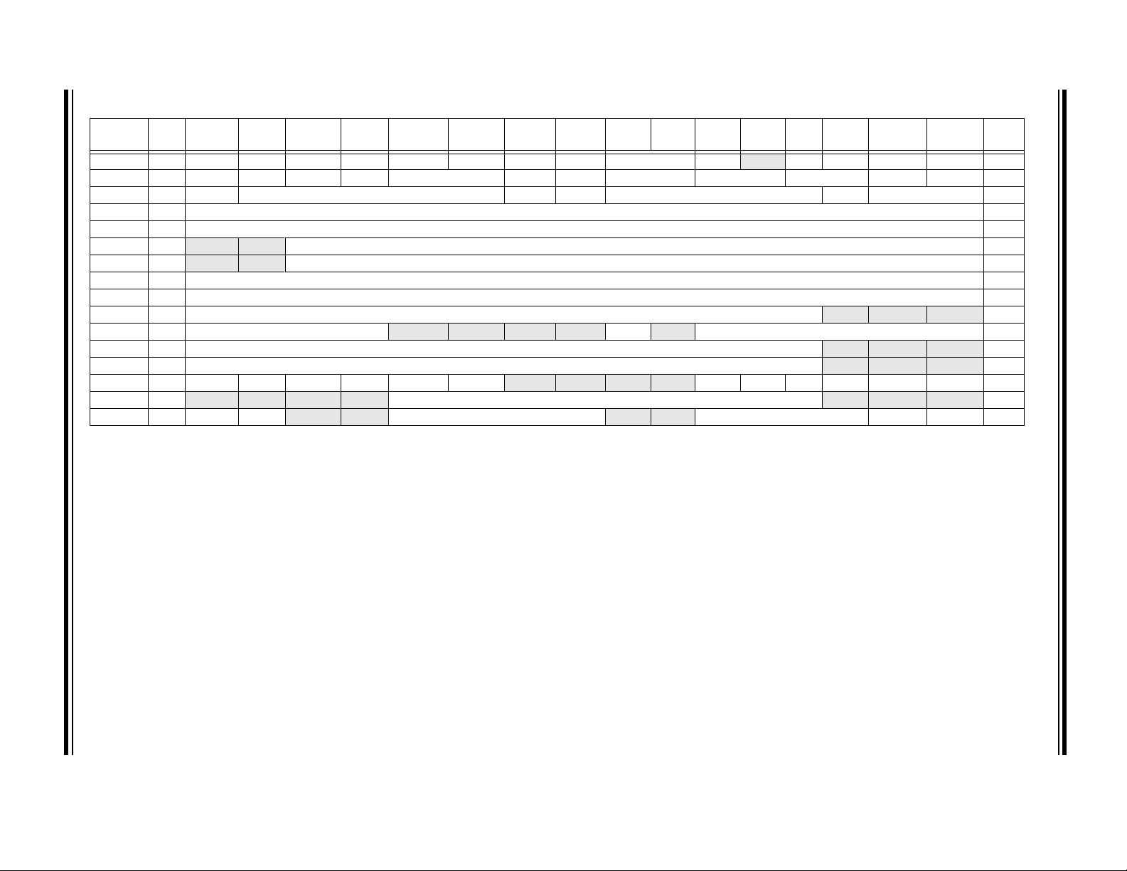
DS70591C-page 76 Preliminary 2010 Microchip Technology Inc.
dsPIC33FJ32GS406/606/608/610 and dsPIC33FJ64GS406/606/608/610
TABLE 4-20: HIGH-SPEED PWM GENERATOR 4 REGISTER MAP
File Name
PWMCON4
IOCON4
FCLCON4
PDC4
PHASE4
DTR4
ALTDTR4
SDC4
SPHASE4
TRIG4
TRGCON4
STRIG4
PWMCAP4
LEBCON4
LEBDLY4
AUXCON4
Legend: x = unknown value on Reset, — = unimplemented, read as ‘0’. Reset values are shown in hexadecimal.
Addr
Offset
0480 FLTSTAT CLSTAT TRGSTAT FLTIEN CLIEN TRGIEN ITB MDCS DTC<1:0> DTCP — MTBS CAM XPRES IUE 0000
0482 PENH PENL POLH POLL PMOD<1:0> OVRENH OVRENL OVRDAT<1:0> FLTDAT<1:0> CLDAT <1:0> SWAP OSYNC 0000
0484 IFLTMOD CLSRC<4:0> CLPOL CLMOD FLTSRC<4:0> FLTPOL FLTMOD<1:0> 0000
0486 PDC4<15:0> 0000
0488 PHASE4<15:0> 0000
048A — — DTR4<13:0> 0000
048A — — ALTDTR4<13:0> 0000
048E SDC4<15:0> 0000
0490 SPHASE4<15:0> 0000
0492 TRGCMP<15:3> — — — 0000
0494 TRGDIV<3:0> — — — —DTM—TRGSTRT<5:0>0000
0496 STRGCMP<15:3> — — — 0000
0498 PWMCAP4<15:3> — — — 0000
049A PHR PHF PLR PLF FLTLEBEN CLLEBEN — — — — BCH BCL BPHH BPHL BPLH BPLL 0000
049C — — — — LEB<11:3> — — — 0000
049E HRPDIS HRDDIS — — BLANKSEL<3:0> — — CHOPSEL<3:0> CHOPHEN CHOPLEN 0000
Bit 15 Bit 14 Bit 13 Bit 12 Bit 11 Bit 10 Bit 9 Bit 8 Bit 7 Bit 6 Bit 5 Bit 4 Bit 3 Bit 2 Bit 1 Bit 0
All
Resets
Page 77

2010 Microchip Technology Inc. Preliminary DS70591C-page 77
TABLE 4-21: HIGH-SPEED PWM GENERATOR 5 REGISTER MAP
File Name
PWMCON5
IOCON5
FCLCON5
PDC5
PHASE5
DTR5
ALTDTR5
SDC5
SPHASE5
TRIG5
TRGCON5
STRIG5
PWMCAP5
LEBCON5
LEBDLY5
AUXCON5
Legend: x = unknown value on Reset, — = unimplemented, read as ‘0’. Reset values are shown in hexadecimal.
Addr
Offset
04A0 FLTSTAT CLSTAT TRGSTAT FLTIEN CLIEN TRGIEN ITB MDCS DTC<1:0> DTCP — MTBS CAM XPRES IUE 0000
04A2 PENH PENL POLH POLL PMOD<1:0> OVRENH OVRENL OVRDAT<1:0> FLTDAT<1:0> CLDAT<1:0> SWAP OSYNC 0000
04A4 IFLTMOD CLSRC<4:0> CLPOL CLMOD FLTSRC<4:0> FLTPOL FLTMOD<1:0> 0000
04A6 PDC5<15:0> 0000
04A8 PHASE5<15:0> 0000
04AA — — DTR5<13:0> 0000
04AA — — ALTDTR5<13:0> 0000
04AE SDC5<15:0> 0000
04B0 SPHASE5<15:0> 0000
04B2 TRGCMP<15:3> — — — 0000
04B4 TRGDIV<3:0> — — — —DTM—TRGSTRT<5:0>0000
04B6 STRGCMP<15:3> — — — 0000
04B8 PWMCAP5<15:3> — — — 0000
04BA PHR PHF PLR PLF FLTLEBEN CLLEBEN — — — — BCH BCL BPHH BPHL BPLH BPLL 0000
04BC — — — — LEB<11:3> — — — 0000
04BE HRPDIS HRDDIS — — BLA NKSEL<3:0> — — CHOPSEL<3:0> CHOPHEN CHOPLEN 0000
Bit 15 Bit 14 Bit 13 Bit 12 Bit 11 Bit 10 Bit 9 Bit 8 Bit 7 Bit 6 Bit 5 Bit 4 Bit 3 Bit 2 Bit 1 Bit 0
dsPIC33FJ32GS406/606/608/610 and dsPIC33FJ64GS406/606/608/610
All
Resets
Page 78

DS70591C-page 78 Preliminary 2010 Microchip Technology Inc.
dsPIC33FJ32GS406/606/608/610 and dsPIC33FJ64GS406/606/608/610
TABLE 4-22: HIGH-SPEED PWM GENERATOR 6 REGISTER MAP
File Name
PWMCON6
IOCON6
FCLCON6
PDC6
PHASE6
DTR6
ALTDTR6
SDC6
SPHASE6
TRIG6
TRGCON6
STRIG6
PWMCAP6
LEBCON6
LEBDLY6
AUXCON6
Legend: x = unknown value on Reset, — = unimplemented, read as ‘0’. Reset values are shown in hexadecimal.
Addr
Offset
04C0 FLTSTAT CLSTAT TRGSTAT FLTIEN CLIEN TRGIEN ITB MDCS DTC<1:0> DTCP — MTBS CAM XPRES IUE 0000
04C2 PENH PENL POLH POLL PMOD<1:0> OVRENH OVRENL OVRDAT<1:0> FLTDAT<1:0> CLDAT<1:0> SWAP OSYNC 0000
04C4 IFLTMOD CLSRC<4:0> CLPOL CLMOD FLTSRC<4:0> FLTPOL FLTMOD<1:0> 0000
04C6 PDC6<15:0> 0000
04C8 PHASE6<15:0> 0000
04CA — — DTR6<13:0> 0000
04CA — — ALTDTR6<13:0> 0000
04CE SDC6<15:0> 0000
04D0 SPHASE6<15:0> 0000
04D2 TRGCMP<15:3> — — — 0000
04D4 TRGDIV<3:0> — — — —DTM—TRGSTRT<5:0>0000
04D6 STRGCMP<15:3> — — — 0000
04D8 PWMCAP6<15:3> — — — 0000
04DA PHR PHF PLR PLF FLTLEBEN CLLEBEN — — — — BCH BCL BPHH BPHL BPLH BPLL 0000
04DC — — — — LEB<11:3> — — — 0000
04DE HRPDIS HRDDIS — — BLANKSEL<3:0> — — CHOPSEL<3:0> CHOPHEN CHOPLEN 0000
Bit 15 Bit 14 Bit 13 Bit 12 Bit 11 Bit 10 Bit 9 Bit 8 Bit 7 Bit 6 Bit 5 Bit 4 Bit 3 Bit 2 Bit 1 Bit 0
All
Resets
Page 79

2010 Microchip Technology Inc. Preliminary DS70591C-page 79
TABLE 4-23: HIGH-SPEED PWM GENERATOR 7 REGISTER MAP (EXCLUDES dsPIC33FJ32GS406 AND dsPIC33FJ64GS406 DEVICES)
File Name
PWMCON7
IOCON7
FCLCON7
PDC7
PHASE7
DTR7
ALTDTR7
SDC7
SPHASE7
TRIG7
TRGCON7
STRIG7
PWMCAP7
LEBCON7
LEBDLY7
AUXCON7
Legend: x = unknown value on Reset, — = unimplemented, read as ‘0’. Reset values are shown in hexadecimal.
Addr
Offset
04E0 FLTSTAT CLSTAT TRGSTAT FLTIEN CLIEN TRGIEN ITB MDCS DTC<1:0> DTCP — MTBS CAM XPRES IUE 0000
04E2 PENH PENL POLH POLL PMOD<1:0> OVRENH OVRENL OVRDAT<1:0> FLTDAT<1:0> CLDAT<1:0> SWAP OSYNC 0000
04E4 IFLTMOD CLSRC<4:0> CLPOL CLMOD FLTSRC<4:0> FLTPOL FLTMOD<1:0> 0000
04E6 PDC7<15:0> 0000
04E8 PHASE7<15:0> 0000
04EA — — DTR7<13:0> 0000
04EA — — ALTDTR7<13:0> 0000
04EE SDC7<15:0> 0000
04F0 SPHASE7<15:0> 0000
04F2 TRGCMP<15:3> — — — 0000
04F4 TRGDIV<3:0> — — — —DTM—TRGSTRT<5:0>0000
04F6 STRGCMP<15:3> — — — 0000
04F8 PWMCAP7<15:3> — — — 0000
04FA PHR PHF PLR PLF FLTLEBEN CLLEBEN — — — — BCH BCL BPHH BPHL BPLH BPLL 0000
04FC — — — — LEB<11:3> — — — 0000
04FE HRPDIS HRDDIS — — BLANKSEL<3:0> — — CHOPSEL<3:0> CHOPHEN CHOPLEN 0000
Bit 15 Bit 14 Bit 13 Bit 12 Bit 11 Bit 10 Bit 9 Bit 8 Bit 7 Bit 6 Bit 5 Bit 4 Bit 3 Bit 2 Bit 1 Bit 0
Resets
dsPIC33FJ32GS406/606/608/610 and dsPIC33FJ64GS406/606/608/610
All
Page 80

DS70591C-page 80 Preliminary 2010 Microchip Technology Inc.
dsPIC33FJ32GS406/606/608/610 and dsPIC33FJ64GS406/606/608/610
TABLE 4-24: HIGH-SPEED PWM GENERATOR 8 REGISTER MAP (EXCLUDES dsPIC33FJ32GS406 AND dsPIC33FJ64GS406 DEVICES)
File Name
PWMCON8
IOCON8
FCLCON8
PDC8
PHASE8
DTR8
ALTDTR8
SDC8
SPHASE8
TRIG8
TRGCON8
STRIG8
PWMCAP8
LEBCON8
LEBDLY8
AUXCON8
Legend: x = unknown value on Reset, — = unimplemented, read as ‘0’. Reset values are shown in hexadecimal.
Addr
Offset
0500 FLTSTAT CLSTAT TRGSTAT FLTIEN CLIEN TRGIEN ITB MDCS DTC<1:0> DTCP — MTBS CAM XPRES IUE 0000
0502 PENH PENL POLH POLL PMOD<1:0> OVRENH OVRENL OVRDAT<1:0> FLTDAT<1:0> CLDAT <1:0> SWAP OSYNC 0000
0504 IFLTMOD CLSRC<4:0> CLPOL CLMOD FLTSRC<4:0> FLTPOL FLTMOD<1:0> 0000
0506 PDC8<15:0> 0000
0508 PHASE8<15:0> 0000
050A — — DTR8<13:0> 0000
050A — — ALTDTR8<13:0> 0000
050E SDC8<15:0> 0000
0510 SPHASE8<15:0> 0000
0512 TRGCMP<15:3> — — — 0000
0514 TRGDIV<3:0> — — — —DTM—TRGSTRT<5:0>0000
0516 STRGCMP<15:3> — — — 0000
0518 PWMCAP8<15:3> — — — 0000
051A PHR PHF PLR PLF FLTLEBEN CLLEBEN — — — — BCH BCL BPHH BPHL BPLH BPLL 0000
051C — — — — LEB<11:3> — — — 0000
051E HRPDIS HRDDIS — — BLANKSEL<3:0> — — CHOPSEL<3:0> CHOPHEN CHOPLEN 0000
Bit 15 Bit 14 Bit 13 Bit 12 Bit 11 Bit 10 Bit 9 Bit 8 Bit 7 Bit 6 Bit 5 Bit 4 Bit 3 Bit 2 Bit 1 Bit 0
All
Resets
Page 81

2010 Microchip Technology Inc. Preliminary DS70591C-page 81
TABLE 4-25: HIGH-SPEED PWM GENERATOR 9 REGISTER MAP FOR dsPIC33FJ32GS610 AND dsPIC33FJ64GS610 DEVICES
File Name
PWMCON9
IOCON9
FCLCON9
PDC9
PHASE9
DTR9
ALTDTR9
SDC9
SPHASE9
TRIG9
TRGCON9
STRIG9
PWMCAP9
LEBCON9
LEBDLY9
AUXCON9
Legend: x = unknown value on Reset, — = unimplemented, read as ‘0’. Reset values are shown in hexadecimal.
Addr
Offset
0520 FLTSTAT CLSTAT TRGSTAT FLTIEN CLIEN TRGIEN ITB MDCS DTC<1:0> DTCP — MTBS CAM XPRES IUE 0000
0522 PENH PENL POLH POLL PMOD<1:0> OVRENH OVRENL OVRDAT<1:0> FLTDAT<1:0> CLDAT <1:0> SWAP OSYNC 0000
0524 IFLTMOD CLSRC<4:0> CLPOL CLMOD FLTSRC<4:0> FLTPOL FLTMOD<1:0> 0000
0526 PDC9<15:0> 0000
0528 PHASE9<15:0> 0000
052A — — DTR9<13:0> 0000
052A — — ALTDTR9<13:0> 0000
052E SDC9<15:0> 0000
0530 SPHASE9<15:0> 0000
0532 TRGCMP<15:3> — — — 0000
0534 TRGDIV<3:0> — — — —DTM—TRGSTRT<5:0>0000
0536 STRGCMP<15:3> — — — 0000
0538 PWMCAP9<15:3> — — — 0000
053A PHR PHF PLR PLF FLTLEBEN CLLEBEN — — — — BCH BCL BPHH BPHL BPLH BPLL 0000
053C — — — — LEB<11:3> — — — 0000
053E HRPDIS HRDDIS — — BLANKSEL<3:0> — — CHOPSEL<3:0> CHOPHEN CHOPLEN 0000
Bit 15 Bit 14 Bit 13 Bit 12 Bit 11 Bit 10 Bit 9 Bit 8 Bit 7 Bit 6 Bit 5 Bit 4 Bit 3 Bit 2 Bit 1 Bit 0
TABLE 4-26: I2C1 REGISTER MAP
SFR Name
I2C1RCV 0200 — — — — — — — — Receive Register
I2C1TRN 0202 — — — — — — — — Transmit Register
I2C1BRG 0204 — — — — — — — Baud Rate G ene rator Re gist er
I2C1CON 0206 I2CEN — I2CSIDL SCLREL IPMIEN A10M DISSLW SMEN GCEN STREN ACKDT ACKEN RCEN PEN RSEN SEN
I2C1STA T 0208 ACKSTA T TRSTA T — — — BCL GCST AT ADD10 IWCOL I2COV D_A P S R_W RBF TBF
I2C1ADD 020A — — — — — —Address Register
I2C1MSK 020C — — — — — — Address M a sk Re g is ter
Legend: x = unknown value on Reset, — = unimplemented, read as ‘0’. Reset values are shown in hexadecimal.
SFR
Addr
Bit 15 Bit 14 Bit 13 Bit 12 Bit 11 Bit 10 Bit 9 Bit 8 Bit 7 Bit 6 Bit 5 Bit 4 Bit 3 Bit 2 Bit 1 Bit 0
All
Resets
All
Resets
0000
00FF
0000
1000
0000
0000
0000
dsPIC33FJ32GS406/606/608/610 and dsPIC33FJ64GS406/606/608/610
Page 82

DS70591C-page 82 Preliminary 2010 Microchip Technology Inc.
dsPIC33FJ32GS406/606/608/610 and dsPIC33FJ64GS406/606/608/610
TABLE 4-27: I2C2 REGISTER MAP
SFR Name
I2C2RCV 0210 — — — — — — — — Receive Register
I2C2TRN 0212 — — — — — — — — Transmit Register
I2C2BRG 0214 — — — — — — — Baud Rate Gene ra tor R e gister
I2C2CON 0216 I2CEN — I2CSIDL SCLREL IPMIEN A10M DISSL W SMEN GCEN STREN ACKDT ACKEN RCEN PEN RSEN SEN
I2C2STA T 0218 ACKSTAT TRSTAT — — — BCL GCST A T ADD10 IWCOL I2COV D_A P S R_W RBF TBF
I2C2ADD 021A — — — — — —Address Register
I2C2MSK 021C — — — — — — Address Ma sk R e gis ter
Legend: x = unknown value on Reset, — = unimplemented, read as ‘0’. Reset values are shown in hexadecimal.
SFR
Addr
Bit 15 Bit 14 Bit 13 Bit 12 Bit 11 Bit 10 Bit 9 Bit 8 Bit 7 Bit 6 Bit 5 Bit 4 Bit 3 Bit 2 Bit 1 Bit 0
All
Resets
0000
00FF
0000
1000
0000
0000
0000
TABLE 4-28: UART1 REGISTER MAP
SFR Name
U1MODE 0220 UARTEN — USIDL IREN RTSMD — UEN1 UEN0 WAKE LPBACK ABAUD URXINV BRGH PDSEL<1:0> STSEL
U1STA 0222 UTXISEL1 UTXINV UTXISEL0 — UTXBRK UTXEN UTXBF TRMT URXISEL<1:0> ADDEN RIDLE PERR FERR OERR URXDA
U1TXREG 0224 — — — — — — — UART Transmit Regis ter
U1RXREG 0226 — — — — — — — UART Receive Register
U1BRG 0228 Baud Ra te G en er a tor Prescaler
Legend: x = unknown value on Reset, — = unimplemented, read as ‘0’. Reset values are shown in hexadecimal.
SFR
Addr
Bit 15 Bit 14 Bit 13 Bit 12 Bit 11 Bit 10 Bit 9 Bit 8 Bit 7 Bit 6 Bit 5 Bit 4 Bit 3 Bit 2 Bit 1 Bit 0
All
Resets
0000
0110
xxxx
0000
0000
TABLE 4-29: UART2 REGISTER MAP
SFR
Name
U2MODE 0230 UARTEN — USIDL IREN RTSMD — UEN1 UEN0 WAKE LPBACK ABAUD URXINV BRGH PDSEL<1:0> STSEL
U2STA 0232 UTXISEL1 UTXINV UTXISEL0 — UTXBRK UTXEN UTXBF TRMT URXISEL<1:0> ADDEN RIDLE PERR FERR OERR URXDA
U2TXREG 0234 — — — — — — — UART Tr an smi t Re gister
U2RXREG 0236 — — — — — — — UART Receive R egister
U2BRG 0238 Baud Rate Generator P rescal er
Legend: x = unknown value on Reset, — = unimplemented, read as ‘0’. Reset values are shown in hexadecimal.
SFR
Addr
Bit 15 Bit 14 Bit 13 Bit 12 Bit 11 Bit 10 Bit 9 Bit 8 Bit 7 Bit 6 Bit 5 Bit 4 Bit 3 Bit 2 Bit 1 Bit 0
All
Resets
0000
0110
xxxx
0000
0000
Page 83

2010 Microchip Technology Inc. Preliminary DS70591C-page 83
TABLE 4-30: SPI1 REGISTER MAP
SFR Name
SPI1STAT 0240 SPIEN — SPISIDL — — — — — —SPIROV— — — — SPITBF SPIRBF
SPI1CON1 0242 — — — DISSCK DISSDO MODE16 SMP CKE SSEN CKP MSTEN SPRE<2:0> PPRE<1:0>
SPI1CON2 0244 FRMEN SPIFSD FRMPOL — — — — — — — — — — — FRMDLY —
SPI1BUF 0248 SPI1 Transmit and Receive Buffer Register
Legend: x = unknown value on Reset, — = unimplemented, read as ‘0’. Reset values are shown in hexadecimal.
SFR
Addr
Bit 15 Bit 14 Bit 13 Bit 12 Bit 11 Bit 10 Bit 9 Bit 8 Bit 7 Bit 6 Bit 5 Bit 4 Bit 3 Bit 2 Bit 1 Bit 0
TABLE 4-31: SPI2 REGISTER MAP
SFR Name
SPI2STAT 0260 SPIEN — SPISIDL — — — — — —SPIROV— — — — SPITBF SPIRBF
SPI2CON1 0262 — — — DISSCK DISSDO MODE16 SMP CKE SSEN CKP MSTEN SPRE<2:0> PPRE<1:0>
SPI2CON2 0264 FRMEN SPIFSD FRMPOL — — — — — — — — — — — FRMDLY —
SPI2BUF 0268 SPI2 Transmit and Receive Buffer Register
Legend: x = unknown value on Reset, — = unimplemented, read as ‘0’. Reset values are shown in hexadecimal.
SFR
Addr
Bit 15 Bit 14 Bit 13 Bit 12 Bit 11 Bit 10 Bit 9 Bit 8 Bit 7 Bit 6 Bit 5 Bit 4 Bit 3 Bit 2 Bit 1 Bit 0
dsPIC33FJ32GS406/606/608/610 and dsPIC33FJ64GS406/606/608/610
All
Resets
0000
0000
0000
0000
All
Resets
0000
0000
0000
0000
Page 84

DS70591C-page 84 Preliminary 2010 Microchip Technology Inc.
dsPIC33FJ32GS406/606/608/610 and dsPIC33FJ64GS406/606/608/610
TABLE 4-32: HIGH-SPEED 10-BIT ADC REGISTER MAP FOR dsPIC33FJ32GS610 AND dsPIC33FJ64GS610 DEVICES ONLY
SFR Name
ADCON 0300 ADON
ADPCFG 0302 PCFG15 PCFG14 PCFG13 PCFG12 PCFG11 PCFG10 PCFG9 PCFG8 PCFG7 PCFG6 PCFG5 PCFG4 PCFG3 PCFG2 PCFG1 PCFG0 0000
ADPCFG2 0304
ADSTAT 0306
ADBASE 0308 ADBASE<15:1>
ADCPC0 030A IRQEN1 PEND1 SWTRG1 TRGSRC1<4:0> IRQEN0 PEND0 SWTRG0 TRGSRC0<4:0> 0000
ADCPC1 030C IRQEN3 PEND3 SWTRG3 TRGSRC3<4:0> IRQEN2 PEND2 SWTRG2 TRGSRC2<4:0> 0000
ADCPC2 030E IRQEN5 PEND5 SWTRG5 TRGSRC5<4:0> IRQEN4 PEND4 SWTRG4 TRGSRC4<4:0> 0000
ADCPC3 0310 IRQEN7 PEND7 SWTRG7 TRGSRC7<4:0> IRQEN6 PEND6 SWTRG6 TRGSRC6<4:0> 0000
ADCPC4 0312 IRQEN9 PEND9 SWTRG9 TRGSRC9<4:0> IRQEN8 PEND8 SWTRG8 TRGSRC8<4:0> 0000
ADCPC5 0314 IRQ EN 11 PEND11 SWTRG11 TRGSRC11<4:0> IRQEN10 PEND10 SWTRG10 TRGSRC10<4:0> 0000
ADCPC6 0316
ADCBUF0 0340 ADC Data Buffer 0 xxxx
ADCBUF1 0342 ADC Data Buffer 1 xxxx
ADCBUF2 0344 ADC Data Buffer 2 xxxx
ADCBUF3 0346 ADC Data Buffer 3 xxxx
ADCBUF4 0348 ADC Data Buffer 4 xxxx
ADCBUF5 034A ADC Data Buffer 5 xxxx
ADCBUF6 034C ADC Data Buffer 6 xxxx
ADCBUF7 034E ADC Data Buffer 7 xxxx
ADCBUF8 0350 ADC Data Buffer 8 xxxx
ADCBUF9 0352 ADC Data Buffer 9 xxxx
ADCBUF10 0354 ADC Data Buffer 10 xxxx
ADCBUF11 0356 ADC Data Buffer 11 xxxx
ADCBUF12 0358 ADC Data Buffer 12 xxxx
ADCBUF13 035A ADC Data Buffer 13 xxxx
ADCBUF14 035C ADC Data Buffer 14 xxxx
ADCBUF15 035E ADC Data Buffer 15 xxxx
ADCBUF16 0360 ADC Data Buffer 16 xxxx
ADCBUF17 0362 ADC Data Buffer 17 xxxx
ADCBUF18 0364 ADC Data Buffer 18 xxxx
ADCBUF19 0366 ADC Data Buffer 19 xxxx
ADCBUF20 0368 ADC Data Buffer 20 xxxx
ADCBUF21 036A ADC Data Buffer 21 xxxx
Legend: x = unknown value on Reset, — = unimplemented, read as ‘0’. Reset values are shown in hexadecimal.
SFR
Bit 15 Bit 14 Bit 13 Bit 12 Bit 11 Bit 10 Bit 9 Bit 8 Bit 7 Bit 6 Bit 5 Bit 4 Bit 3 Bit 2 Bit 1 Bit 0
Addr
— ADSIDL SLOWCLK —GSWTRG— FORM EIE ORDER SEQSAMP ASYNCSAMP — ADCS<2:0> 0003
— — — — — — — —
— — —
— — — — — — — —
P12RDY P11RDY P10RDY P9RDY P8RDY P7RDY P6RDY P5RDY P4RDY P3RDY P2RDY P1RDY P0RDY 0000
PCFG23 PCFG22 PCFG21 PCFG20 PCFG19 PCFG18 PCFG17 PCFG16 0000
IRQEN12 PEND12 SWTRG12 TRGSRC12<4:0> 0000
All
Resets
—
0000
Page 85

2010 Microchip Technology Inc. Preliminary DS70591C-page 85
TABLE 4-32: HIGH-SPEED 10-BIT ADC REGISTER MAP FOR dsPIC33FJ32GS610 AND dsPIC33FJ64GS610 DEVICES ONLY (CONTINUED)
SFR Name
ADCBUF22 036C ADC Data Buffer 22 xxxx
ADCBUF23 036E ADC Data Buffer 23 xxxx
ADCBUF24 0370 ADC Data Buffer 24 xxxx
ADCBUF25 0372 ADC Data Buffer 25 xxxx
Legend: x = unknown value on Reset, — = unimplemented, read as ‘0’. Reset values are shown in hexadecimal.
SFR
Bit 15 Bit 14 Bit 13 Bit 12 Bit 11 Bit 10 Bit 9 Bit 8 Bit 7 Bit 6 Bit 5 Bit 4 Bit 3 Bit 2 Bit 1 Bit 0
Addr
All
Resets
dsPIC33FJ32GS406/606/608/610 and dsPIC33FJ64GS406/606/608/610
Page 86

DS70591C-page 86 Preliminary 2010 Microchip Technology Inc.
dsPIC33FJ32GS406/606/608/610 and dsPIC33FJ64GS406/606/608/610
TABLE 4-33: HIGH-SPEED 10-BIT ADC REGISTER MAP FOR dsPIC33FJ32GS608 AND dsPIC33FJ64GS608 DEVICES
SFR Name
ADCON 0300 ADON
ADPCFG 0302 PCFG15 PCFG14 PCFG13 PCFG12 PCFG11 PCFG10 PCFG9 PCFG8 PCFG7 PCFG6 PCFG5 PCFG4 PCFG3 PCFG2 PCFG1 PCFG0 0000
ADPCFG2 0304
ADSTAT 0306
ADBASE 0308 ADBASE<15:1>
ADCPC0 030A IRQEN1 PEND1 SWTRG1 TRGSRC1<4:0> IRQEN0 PEND0 SWTRG0 TRGSRC0<4:0> 0000
ADCPC1 030C IRQEN3 PEND3 SWTRG3 TRGSRC3<4:0> IRQEN2 PEND2 SWTRG2 TRGSRC2<4:0> 0000
ADCPC2 030E IRQEN5 PEND5 SWTRG5 TRGSRC5<4:0> IRQEN4 PEND4 SWTRG4 TRGSRC4<4:0> 0000
ADCPC3 0310 IRQEN7 PEND7 SWTRG7 TRGSRC7<4:0> IRQEN6 PEND6 SWTRG6 TRGSRC6<4:0> 0000
ADCPC4 0312
ADCPC6 0316
ADCBUF0 0340 ADC Data Buffer 0 xxxx
ADCBUF1 0342 ADC Data Buffer 1 xxxx
ADCBUF2 0344 ADC Data Buffer 2 xxxx
ADCBUF3 0346 ADC Data Buffer 3 xxxx
ADCBUF4 0348 ADC Data Buffer 4 xxxx
ADCBUF5 034A ADC Data Buffer 5 xxxx
ADCBUF6 034C ADC Data Buffer 6 xxxx
ADCBUF7 034E ADC Data Buffer 7 xxxx
ADCBUF8 0350 ADC Data Buffer 8 xxxx
ADCBUF9 0352 ADC Data Buffer 9 xxxx
ADCBUF10 0354 ADC Data Buffer 10 xxxx
ADCBUF11 0356 ADC Data Buffer 11 xxxx
ADCBUF12 0358 ADC Data Buffer 12 xxxx
ADCBUF13 035A ADC Data Buffer 13 xxxx
ADCBUF14 035C ADC Data Buffer 14 xxxx
ADCBUF15 035E ADC Data Buffer 15 xxxx
ADCBUF16 0360 ADC Data Buffer 16 xxxx
ADCBUF17 0362 ADC Data Buffer 17 xxxx
ADCBUF24 0370 ADC Data Buffer 24 xxxx
ADCBUF25 0372 ADC Data Buffer 25 xxxx
Legend: x = unknown value on Reset, — = unimplemented, read as ‘0’. Reset values are shown in hexadecimal.
SFR
Bit 15 Bit 14 Bit 13 Bit 12 Bit 11 Bit 10 Bit 9 Bit 8 Bit 7 Bit 6 Bit 5 Bit 4 Bit 3 Bit 2 Bit 1 Bit 0
Addr
—ADSIDLSLOWCLK—GSWTRG— FORM EIE ORDER SEQSAMP ASYNCSAMP — ADCS<2:0> 0003
— — — — — — — — — — — — — — PCFG17 PCFG16 0000
— — — P12RDY — — — P8RDY P7RDY P6RDY P5RDY P4RDY P3RDY P2RDY P1RDY P0RDY 0000
— — — — — — — — IRQEN8 PEND8 SWTRG8 TRGSRC8<4:0> 0000
— — — — — — — —
IRQEN12 PEND12 S WTRG12 TRGSRC12<4:0> 0000
All
Resets
— 0000
Page 87

2010 Microchip Technology Inc. Preliminary DS70591C-page 87
TABLE 4-34: HIGH-SPEED 10-BIT ADC REGISTER MAP FOR dsPIC33FJ32GS406/606 AND dsPIC33FJ64GS406/606 DEVICES
SFR Name
ADCON 0300 ADON
ADPCFG 0302 PCFG15 PCFG14 PCFG13 PCFG12 PCFG11 PCFG10 PCFG9 PCFG8 PCFG7 PCFG6 PCFG5 PCFG4 PCFG3 PCFG2 PCFG1 PCFG0 0000
ADSTAT 0306
ADBASE 0308 ADBASE<15:1>
ADCPC0 030A IRQEN1 PEND1 SWTRG1 TRGSRC1<4:0> IRQEN0 PEND0 SWTRG0 TRGSRC0<4:0> 0000
ADCPC1 030C IRQEN3 PEND3 SWTRG3 TRGSRC3<4:0> IRQEN2 PEND2 SWTRG2 TRGSRC2<4:0> 0000
ADCPC2 030E IRQEN5 PEND5 SWTRG5 TRGSRC5<4:0> IRQEN4 PEND4 SWTRG4 TRGSRC4<4:0> 0000
ADCPC3 0310 IRQEN7 PEND7 SWTRG7 TRGSRC7<4:0> IRQEN6 PEND6 SWTRG6 TRGSRC6<4:0> 0000
ADCPC6 0316
ADCBUF0 0340 ADC Data Buffer 0 xxxx
ADCBUF1 0342 ADC Data Buffer 1 xxxx
ADCBUF2 0344 ADC Data Buffer 2 xxxx
ADCBUF3 0346 ADC Data Buffer 3 xxxx
ADCBUF4 0348 ADC Data Buffer 4 xxxx
ADCBUF5 034A ADC Data Buffer 5 xxxx
ADCBUF6 034C ADC Data Buffer 6 xxxx
ADCBUF7 034E ADC Data Buffer 7 xxxx
ADCBUF8 0350 ADC Data Buffer 8 xxxx
ADCBUF9 0352 ADC Data Buffer 9 xxxx
ADCBUF10 0354 ADC Data Buffer 10 xxxx
ADCBUF11 0356 ADC Data Buffer 11 xxxx
ADCBUF12 0358 ADC Data Buffer 12 xxxx
ADCBUF13 035A ADC Data Buffer 13 xxxx
ADCBUF14 035C ADC Data Buffer 14 xxxx
ADCBUF15 035E ADC Data Buffer 15 xxxx
ADCBUF24 0370 ADC Data Buffer 24 xxxx
ADCBUF25 0372 ADC Data Buffer 25 xxxx
Legend: x = unknown value on Reset, — = unimplemented, read as ‘0’. Reset values are shown in hexadecimal.
SFR
Bit 15 Bit 14 Bit 13 Bit 12 Bit 11 Bit 10 Bit 9 Bit 8 Bit 7 Bit 6 Bit 5 Bit 4 Bit 3 Bit 2 Bit 1 Bit 0
Addr
— ADSIDL SLOWCLK —GSWTRG— FORM EIE ORDER SEQSAMP ASYNCSAMP — ADCS<2:0> 0003
— — —P12RDY— — — — P7RDY
— — — — — — — —
IRQEN12 PEND12 SWTRG12 TRGSRC12<4:0> 0000
P6RDY P5RDY P4RDY P3RDY P2RDY P1RDY P0RDY 0000
—
All
Resets
0000
dsPIC33FJ32GS406/606/608/610 and dsPIC33FJ64GS406/606/608/610
Page 88

DS70591C-page 88 Preliminary 2010 Microchip Technology Inc.
dsPIC33FJ32GS406/606/608/610 and dsPIC33FJ64GS406/606/608/610
TABLE 4-35: DMA REGISTER MAP
File Name Addr Bit 15 Bit 14 Bit 13 Bit 12 Bit 11 Bit 10 Bit 9 Bit 8 Bit 7 Bit 6 Bit 5 Bit 4 Bit 3 Bit 2 Bit 1 Bit 0
DMA0CON 0380 CHEN SIZE DIR HALF NULLW
DMA0REQ 0382 FORCE
DMA0STA 0384 STA<15:0> 0000
DMA0STB 0386 STB<15:0> 0000
DMA0PAD 0388 PAD<15:0> 0000
DMA0CNT 038A
DMA1CON 038C CHEN S IZE DIR HALF NULLW
DMA1REQ 0 38 E FORCE
DMA1STA 0390 STA<15:0> 0000
DMA1STB 0392 STB<15:0> 0000
DMA1PAD 0394 PAD<15:0> 0000
DMA1CNT 0396
DMA2CON 0398 CHEN SIZE DIR HALF NULLW
DMA2REQ 039A FORCE
DMA2STA 039C STA<15:0> 0000
DMA2STB 039E STB<15:0> 0000
DMA2PAD 03A0 PAD<15:0> 0000
DMA2CNT 03A2
DMA3CON 03A4 CHEN SIZE DIR HALF NULLW
DMA3REQ 03A6 FORCE
DMA3STA 03A8 STA<15:0> 0000
DMA3STB 03AA STB<15:0> 0000
DMA3PAD 03AC PAD<15:0> 0000
DMA3CNT 03AE
DMACS0 03E0
DMACS1 03E2
DSADR 03E4 DSADR<15:0> 0000
Legend: — = unimplemented, read as ‘0’. Reset values are shown in hexadecimal.
— — — — — — CNT<9:0> 0000
— — — — — — CNT<9:0> 0000
— — — — — — CNT<9:0> 0000
— — — — — — CNT<9:0> 0000
— — — — PWCOL3 PWCOL2 PWCOL1 PWCOL0 — — — — XWCOL3 XWCOL2 XWCOL1 XWCOL0 0000
— — — — LSTCH<3:0> — — — — PPST3 PPST2 PPST1 PPST0 0F00
— — — — — — — — IRQSEL<6:0> 007F
— — — — — — — — IRQSEL<6:0> 007F
— — — — — — — — IRQSEL<6:0> 007F
— — — — — — — — IRQSEL<6:0> 007F
— — — — —AMODE<1:0>— —MODE<1:0>0000
— — — — —AMODE<1:0>— —MODE<1:0>0000
— — — — —AMODE<1:0>— —MODE<1:0>0000
— — — — —AMODE<1:0>— —MODE<1:0>0000
All
Resets
Page 89

2010 Microchip Technology Inc. Preliminary DS70591C-page 89
TABLE 4-36: ECAN1 REGISTER MAP WHEN C1CTRL1.WIN = 0 OR 1
File Name Addr Bit 15 Bit 14 Bit 13 Bit 12 Bit 11 Bit 10 Bit 9 Bit 8 Bit 7 Bit 6 Bit 5 Bit 4 Bit 3 Bit 2 Bit 1 Bit 0
C1CTRL1 0600
C1CTRL2 0602
C1VEC 0604
C1FCTRL 0606 DMABS<2:0>
C1FIFO 0608
C1INTF 060A
C1INTE 060C
C1EC 060E TERRCNT<7:0> RERRCNT<7:0> 0000
C1CFG1 0610
C1CFG2 0612
C1FEN1 0614
C1FMSKSEL1 0618 F7MSK<1:0> F6MSK<1:0> F5MSK<1:0> F4MSK<1:0> F3MSK<1:0> F2MSK<1:0> F1MSK<1:0> F0MSK<1:0> 0000
C1FMSKSEL2 061A F15MSK<1:0> F14MSK<1:0> F13MSK<1:0> F12MSK<1:0> F11MSK<1:0> F 10MSK<1:0> F9MSK<1:0> F8MSK<1:0> 0000
Legend: — = unimplemented, read as ‘0’. Reset values are shown in hexadecimal.
— — CSIDL ABAT — REQOP<2:0> OPMODE<2:0> — CANCAP — —WIN0480
— — — — — — — — — — — DNCNT<4:0> 0000
— — —FILHIT<4:0> — ICODE<6:0> 0000
— — — — — — — —
— — FBP<5:0> — — FNRB<5:0> 0000
— — TXBO TXBP RXBP TXWAR RXWAR EWARN IVRIF WAKIF ERRIF — FIFOIF RBOVIF RBIF TBIF 0000
— — — — — — — — IVRIE WAKIE ERRIE — FIFOIE RBOVIE RBIE TBIE 0000
— — — — — — — — SJW<1:0> BRP<5:0> 0000
— WAKFIL — — — SEG2PH<2:0> SEG2PHTS SAM SEG1PH<2:0> PRSEG<2:0> 0000
FLTEN15 FLTEN14 FLTEN13 FLTEN12 FL TEN 11 FLTEN10 FLTEN9 FLTEN8 FLTEN7 FLTEN6 FLTEN5 FLTEN4 FLTEN3 FLTEN2 FLTEN1 FLTEN0
FSA<4:0>
All
Resets
0000
FFFF
TABLE 4-37: ECAN1 REGISTER MAP WHEN C1CTRL1.WIN = 0
File Name Addr Bit 15 Bit 14 Bit 13 Bit 12 Bit 11 Bit 10 Bit 9 Bit 8 Bit 7 Bit 6 Bit 5 Bit 4 Bit 3 Bit 2 Bit 1 Bit 0
0600-
061E
C1RXFUL1 0620 RXFUL15 RXFUL14 RXFUL13 RXFUL12 RXFUL11 RXFUL10 RXFUL9 RXFUL8 RXFUL7 RXFUL6 RXFUL5 RXFUL4 RXFUL3 RXFUL2 RXFUL1 RXFUL0 0000
C1RXFUL2 0622 RXFUL31 RXFUL30 RXFUL29 RXFUL28 RXFUL27 RXFUL26 RXFUL25 RXFUL24 RXFUL23 RXFUL22 RXFUL21 RXFUL20 RXFUL19 RXFUL18 RXFUL17 RXFUL16 0000
C1RXOVF1 0628 RXOVF15 RXOVF14 RXOVF13 RXOVF12 RXOVF11 RXOVF10 RXOVF9 RXOVF8 RXOVF7 RXOVF6 RXOVF5 RXOVF4 RXOVF3 RXOVF2 RXOVF1 RXOVF0 0000
C1RXOVF2 062A RXOVF31 RXOVF30 RXOVF29 RXOVF28 RXOVF27 RXOVF26 RXOVF25 RXOVF24 RXOVF23 RXOVF22 RXOVF21 RXOVF20 RXOVF19 RXOVF18 RXOVF17 RXOVF16 0000
C1TR01CON 0630
C1TR23CON 0632
C1TR45CON 0634
C1TR67CON 0636
C1RXD 0640 Received Data Word xxxx
C1TXD 0642 Transmit Data Word xxxx
Legend: x = unknown value on Reset, — = unimplemented, read as ‘0’. Reset values are shown in hexadecimal.
TXEN1 TXABT1 TXLARB1 TXERR1 TXREQ1 RTREN1 TX1PRI<1:0> TXEN0 TXABT0 TXLARB0 TXERR0 TXREQ0 RTREN0 TX0PRI<1:0>
TXEN3 TXABT3 TXLARB3 TXERR3 TXREQ3 RTREN3 TX3PRI<1:0> TXEN2 TXABT2 TXLARB2 TXERR2 TXREQ2 RTREN2 TX2PRI<1:0>
TXEN5 TXABT5 TXLARB5 TXERR5 TXREQ5 RTREN5 TX5PRI<1:0> TXEN4 TXABT4 TXLARB4 TXERR4 TXREQ4 RTREN4 TX4PRI<1:0>
TXEN7 TXABT7 TXLARB7 TXERR7 TXREQ7 RTREN7 TX7PRI<1:0> TXEN6 TXABT6 TXLARB6 TXERR6 TXREQ6 RTREN6 TX6PRI<1:0>
See definition when WIN = x
All
Resets
0000
0000
0000
0000
dsPIC33FJ32GS406/606/608/610 and dsPIC33FJ64GS406/606/608/610
Page 90

DS70591C-page 90 Preliminary 2010 Microchip Technology Inc.
dsPIC33FJ32GS406/606/608/610 and dsPIC33FJ64GS406/606/608/610
TABLE 4-38: ECAN1 REGISTER MAP WHEN C1CTRL1.WIN = 1
File Name Addr Bit 15 Bit 14 Bit 13 Bit 12 Bit 11 Bit 10 Bit 9 Bit 8 Bit 7 Bit 6 Bit 5 Bit 4 Bit 3 Bit 2 Bit 1 Bit 0
0600-
061E
C1BUFPNT1 0620 F3BP<3:0> F2BP<3:0> F1BP<3:0> F0BP<3:0> 0000
C1BUFPNT2 0622 F7BP<3:0> F6BP<3:0> F5BP<3:0> F4BP<3:0> 0000
C1BUFPNT3 0624 F11BP<3:0> F10BP<3:0> F9BP<3:0> F8BP<3:0> 0000
C1BUFPNT4 0626 F15BP<3:0> F14BP<3:0> F13BP<3:0> F12BP<3:0> 0000
C1RXM0SID 0630 SID<10:3> SID<2:0>
C1RXM0EID 0632 EID<15:8> EID<7:0> xxxx
C1RXM1SID 0634 SID<10:3> SID<2:0>
C1RXM1EID 0636 EID<15:8> EID<7:0> xxxx
C1RXM2SID 0638 SID<10:3> SID<2:0>
C1RXM2EID 063A EID<15:8> EID<7:0> xxxx
C1RXF0SID 0640 SID<10:3> SID<2:0>
C1RXF0EID 0642 EID<15:8> EID<7:0> xxxx
C1RXF1SID 0644 SID<10:3> SID<2:0>
C1RXF1EID 0646 EID<15:8> EID<7:0> xxxx
C1RXF2SID 0648 SID<10:3> SID<2:0>
C1RXF2EID 064A EID<15:8> EID<7:0> xxxx
C1RXF3SID 064C SID<10:3> SID<2:0>
C1RXF3EID 064E EID<15:8> EID<7:0> xxxx
C1RXF4SID 0650 SID<10:3> SID<2:0>
C1RXF4EID 0652 EID<15:8> EID<7:0> xxxx
C1RXF5SID 0654 SID<10:3> SID<2:0>
C1RXF5EID 0656 EID<15:8> EID<7:0> xxxx
C1RXF6SID 0658 SID<10:3> SID<2:0>
C1RXF6EID 065A EID<15:8> EID<7:0> xxxx
C1RXF7SID 065C SID<10:3> SID<2:0>
C1RXF7EID 065E EID<15:8> EID<7:0> xxxx
C1RXF8SID 0660 SID<10:3> SID<2:0>
C1RXF8EID 0662 EID<15:8> EID<7:0> xxxx
C1RXF9SID 0664 SID<10:3> SID<2:0>
C1RXF9EID 0666 EID<15:8> EID<7:0> xxxx
C1RXF10SID 0668 SID<10:3> SID<2:0>
C1RXF10EID 066A EID<15:8> EID<7:0> xxxx
C1RXF11SID 066C SID<10:3> SID<2:0>
Legend: x = unknown value on Reset, — = unimplemented, read as ‘0’. Reset values are shown in hexadecimal.
See definition w hen WIN = x
—MIDE—EID<17:16>xxxx
—MIDE—EID<17:16>xxxx
—MIDE—EID<17:16>xxxx
— EXIDE —EID<17:16>xxxx
— EXIDE —EID<17:16>xxxx
— EXIDE —EID<17:16>xxxx
— EXIDE —EID<17:16>xxxx
— EXIDE —EID<17:16>xxxx
— EXIDE —EID<17:16>xxxx
— EXIDE —EID<17:16>xxxx
— EXIDE —EID<17:16>xxxx
— EXIDE —EID<17:16>xxxx
— EXIDE —EID<17:16>xxxx
— EXIDE —EID<17:16>xxxx
— EXIDE —EID<17:16>xxxx
All
Resets
Page 91

2010 Microchip Technology Inc. Preliminary DS70591C-page 91
TABLE 4-38: ECAN1 REGISTER MAP WHEN C1CTRL1.WIN = 1 (CONTINUED)
File Name Addr Bit 15 Bit 14 Bit 13 Bit 12 Bit 11 Bit 10 Bit 9 Bit 8 Bit 7 Bit 6 Bit 5 Bit 4 Bit 3 Bit 2 Bit 1 Bit 0
C1RXF11EID 066E EID<15:8> EID<7:0> xxxx
C1RXF12SID 0670 SID<10:3> SID<2:0>
C1RXF12EID 0672 EID<15:8> EID<7:0> xxxx
C1RXF13SID 0674 SID<10:3> SID<2:0>
C1RXF13EID 0676 EID<15:8> EID<7:0> xxxx
C1RXF14SID 0678 SID<10:3> SID<2:0>
C1RXF14EID 067A EID<15:8> EID<7:0> xxxx
C1RXF15SID 067C SID<10:3> SID<2:0>
C1RXF15EID 067E EID<15:8> EID<7:0> xxxx
Legend: x = unknown value on Reset, — = unimplemented, read as ‘0’. Reset values are shown in hexadecimal.
— EXIDE —EID<17:16>xxxx
— EXIDE —EID<17:16>xxxx
— EXIDE —EID<17:16>xxxx
— EXIDE —EID<17:16>xxxx
All
Resets
dsPIC33FJ32GS406/606/608/610 and dsPIC33FJ64GS406/606/608/610
Page 92

DS70591C-page 92 Preliminary 2010 Microchip Technology Inc.
TABLE 4-39: ANALOG COMPARATOR CONTROL REGISTER MAP
File Name ADR Bit 15 Bit 14 Bit 13 Bit 12 Bit 11 Bit 10 Bit 9 Bit 8 Bit 7 Bit 6 Bit 5 Bit 4 Bit 3 Bit 2 Bit 1 Bit 0
CMPCON1 0540 CMPON
CMPDAC1 0542
CMPCON2 0544 CMPON
CMPDAC2 0546
CMPCON3 0548 CMPON
CMPDAC3 054A
CMPCON4 054C CMPON
CMPDAC4 054E
— — - — — —CMREF<9:0>0000
— — - — — —CMREF<9:0>0000
— — - — — —CMREF<9:0>0000
— — — — — —CMREF<9:0>0000
— CMPSIDL — — — — DACOE INSEL<1:0> EXTREF — CMPSTAT — CMPPOL RANGE 0000
— CMPSIDL — — — — DACOE INSEL<1:0> EXTREF — CMPSTAT — CMPPOL RANGE 0000
— CMPSIDL — — — — DACOE INSEL<1:0> EXTREF — CMPSTAT — CMPPOL RANGE 0000
— CMPSIDL — — — — DACOE INSEL<1:0> EXTREF — CMPSTAT — CMPPOL RANGE 0000
All
Resets
dsPIC33FJ32GS406/606/608/610 and dsPIC33FJ64GS406/606/608/610
TABLE 4-40: PORTA REGISTER MAP FOR dsPIC33FJ32GS610 AND dsPIC33FJ64GS610 DEVICES
SFR
SFR
Name
TRISA 02C0 TRISA15 TRISA14
PORTA 02C2 RA15 RA14
LATA 02C4 LATA15 LATA14
ODCA 02C6 ODCA15 ODCA14
Legend: x = unknown value on Reset, — = unimplemented, read as ‘0’. Reset values are shown in hexadecimal.
Bit 15 Bit 14 Bit 13 Bit 12 Bit 11 Bit 10 Bit 9 Bit 8 Bit 7 Bit 6 Bit 5 Bit 4 Bit 3 Bit 2 Bit 1 Bit 0
Addr
— — —
— — —
— — —
— — —
TRISA10 TRISA9
RA10 RA9
LATA10 LATA9
ODCA10 ODCA9
—
TRISA7 TRISA6 TRISA5 TRISA4 TRISA3 TRISA2 TRISA1 TRISA0 C6FF
—
—
— — — ODCA5
RA7 RA6 RA5 RA4 RA3 RA2 RA1 RA0 xxxx
LATA7 LATA6 LATA5 LATA4 LATA3 LATA2 LATA1 LATA0 0000
ODCA4
— —
ODCA1 ODCA0 0000
All
Resets
TABLE 4-41: PORTA REGISTER MAP FOR dsPIC33FJ32GS608 AND dsPIC33FJ64GS608 DEVICES
SFR
SFR
Name
TRISA 02C0 TRISA15 TRISA14
PORTA 02C2 RA15 RA14
LATA 02C4 LATA15 LATA14
ODCA 02C6 ODCA15 ODCA14
Legend: x = unknown value on Reset, — = unimplemented, read as ‘0’. Reset values are shown in hexadecimal.
Bit 15 Bit 14 Bit 13 Bit 12 Bit 11 Bit 10 Bit 9 Bit 8 Bit 7 Bit 6 Bit 5 Bit 4 Bit 3 Bit 2 Bit 1 Bit 0
Addr
— — —
— — —
— — —
— — —
TRISA10 TRISA9
RA10 RA9
LATA10 LATA9
ODCA10 ODCA9
— — — — — — — — —
— — — — — — — — —
— — — — — — — — —
— — — — — — — — —
All
Resets
C600
xxxx
0000
0000
Page 93

2010 Microchip Technology Inc. Preliminary DS70591C-page 93
TABLE 4-42: PORTB REGISTER MAP
SFR
Name
TRISB 02C8 TRISB15 TRISB14 TRISB13 TRISB12 TRISB11 TRISB10 TRISB9 TRISB8 TRISB7 TRISB6 TRISB5 TRISB4 TRISB3 TRISB2 TRISB1 TRISB0 FFFF
PORTB 02CA RB15 RB14 RB13 RB12 RB11 RB10 RB9 RB8 RB7 RB6 RB5 RB4 RB3 RB2 RB1 RB0 xxxx
LATB 02CC LATB15 LATB14 LATB13 LATB12 LATB11 LATB10 LATB9 LATB8 LATB7 LATB6 LATB5 LATB4 LATB3 LA TB2 LA TB1 LATB0 0000
Legend: x = unknown value on Reset, — = unimplemented, read as ‘0’. Reset values are shown in hexadecimal.
SFR
Bit 15 Bit 14 Bit 13 Bit 12 Bit 11 Bit 10 Bit 9 Bit 8 Bit 7 Bit 6 Bit 5 Bit 4 Bit 3 Bit 2 Bit 1 Bit 0
Addr
Resets
TABLE 4-43: PORTC REGISTER MAP FOR dsPIC33FJ32GS610 AND dsPIC33FJ64GS610 DEVICES
SFR
Name
TRISC 02D0 T RISC15 TRISC14 TRISC13 TRISC12
PORTC 02D2 RC15 RC14 RC13 RC12
LATC 02D4 LATC15 LATC14 LATC13 LATC12
Legend: x = unknown value on Reset, — = unimplemented, read as ‘0’. Reset values are shown in hexadecimal.
SFR
Addr
Bit 15 Bit 14 Bit 13 Bit 12 Bit 11 Bit 10 Bit 9 Bit 8 Bit 7 Bit 6 Bit 5 Bit 4 Bit 3 Bit 2 Bit 1 Bit 0
— — — — — — —
— — — — — — —
— — — — — — —
TRISC4 TRISC3 TRISC2 TRISC1
RC4 RC3 RC2 RC1
LATC4 LATC3 LATC2 LATC1
—
—
—
Resets
F01E
xxxx
0000
TABLE 4-44: PORTC REGISTER MAP FOR dsPIC33FJ32GS608 AND dsPIC33FJ64GS608 DEVICES
SFR
Name
TRISC 02D0 T RISC15 TRISC14 TRISC13 TRISC12
PORTC 02D2 RC15 RC14 RC13 RC12
LATC 02D4 LATC15 LATC14 LATC13 LATC12
Legend: x = unknown value on Reset, — = unimplemented, read as ‘0’. Reset values are shown in hexadecimal.
SFR
Addr
Bit 15 Bit 14 Bit 13 Bit 12 Bit 11 Bit 10 Bit 9 Bit 8 Bit 7 Bit 6 Bit 5 Bit 4 Bit 3 Bit 2 Bit 1 Bit 0
— — — — — — — — —
— — — — — — — — —
— — — — — — — — —
TRISC2 TRISC1
RC2 RC1
LATC2 LATC1
—
—
—
Resets
F006
xxxx
0000
dsPIC33FJ32GS406/606/608/610 and dsPIC33FJ64GS406/606/608/610
All
All
All
TABLE 4-45: PORTC REGISTER MAP FOR dsPIC33FJ32GS406/606 AND dsPIC33FJ64GS406/606 DEVICES
SFR
Name
TRISC 02D0 T RISC15 TRISC14 TRISC13 TRISC12
PORTC 02D2 RC15 RC14 RC13 RC12
LATC 02D4 LATC15 LATC14 LATC13 LATC12
Legend: x = unknown value on Reset, — = unimplemented, read as ‘0’. Reset values are shown in hexadecimal.
SFR
Addr
Bit 15 Bit 14 Bit 13 Bit 12 Bit 11 Bit 10 Bit 9 Bit 8 Bit 7 Bit 6 Bit 5 Bit 4 Bit 3 Bit 2 Bit 1 Bit 0
— — — — — — — — — — — —
— — — — — — — — — — — —
— — — — — — — — — — — —
All
Resets
F000
xxxx
0000
Page 94

DS70591C-page 94 Preliminary 2010 Microchip Technology Inc.
TABLE 4-46: PORTD REGISTER MAP FOR dsPIC33FJ32GS608/610 AND dsPIC33FJ64GS608/610 DEVICES
SFR
Name
TRISD 02D8 TRISD15 TRISD14 TRISD13 TRISD12 TRISD11 TRISD10 TRISD9 TRISD8 TRISD7 TRISD6 TRISD5 TRISD4 TRISD3 TRISD2 TRISD1 TRISD0 FFFF
PORTD 02DA RD15 RD14 RD13 RD12 RD11 RD10 RD9 RD8 RD7 RD6 RD5 RD4 RD3 RD2 RD1 RD0 xxxx
LATD 02DC LATD15 LATD14 LATD13 LATD12 LATD11 LATD10 LATD9 LATD8 LATD7 LATD6 LATD5 LATD4 LATD3 LATD2 LATD1 LATD0 0000
ODCD 02DE ODC D15 ODCD14 ODCD13 ODCD12 ODCD11 ODCD10 ODCD9 ODCD8 ODCD7 ODCD6 ODCD5 ODCD4 ODCD3 ODCD2 ODCD1 ODCD0 0000
Legend: x = unknown value on Reset, — = unimplemented, read as ‘0’. Reset values are shown in hexadecimal.
SFR
Bit 15 Bit 14 Bit 13 Bit 12 Bit 11 Bit 10 Bit 9 Bit 8 Bit 7 Bit 6 Bit 5 Bit 4 Bit 3 Bit 2 Bit 1 Bit 0
Addr
Resets
All
dsPIC33FJ32GS406/606/608/610 and dsPIC33FJ64GS406/606/608/610
TABLE 4-47: PORTD REGISTER MAP FOR dsPIC33FJ32GS406/606 AND dsPIC33FJ64GS406/606 DEVICES
SFR
Name
TRISD 02D8
PORTD 02DA
LATD 02DC
ODCD 02DE
Legend: x = unknown value on Reset, — = unimplemented, read as ‘0’. Reset values are shown in hexadecimal.
SFR
Bit 15 Bit 14 Bit 13 Bit 12 Bit 11 Bit 10 Bit 9 Bit 8 Bit 7 Bit 6 Bit 5 Bit 4 Bit 3 Bit 2 Bit 1 Bit 0
Addr
— — — —
— — — —
— — — —
— — — —
TRISD11 TRISD10 TRISD9 TRISD8 TRISD7 TRISD6 TRISD5 TRISD4 TRISD3 TRISD2 TRISD1 TRISD0 0FFF
RD11 RD10 RD9 RD8 RD7 RD6 RD5 RD4 RD3 RD2 RD1 RD0 xxxx
LATD11 LATD10 LATD9 LATD8 LATD7 LATD6 LATD5 LATD4 LATD3 LATD2 LATD1 LATD0 0000
ODCD11 ODCD10 ODCD9 ODCD8 ODCD7 ODCD6 ODCD5 ODCD4 ODCD3 ODCD2 ODCD1 ODCD0 0000
All
Resets
TABLE 4-48: PORTE REGISTER MAP FOR dsPIC33FJ32GS608/610 AND dsPIC33FJ64GS608/610 DEVICES
SFR
Name
TRISE 02E0
PORTE 02E2
LATE 02E4
ODCE 02E6
Legend: x = unknown value on Reset, — = unimplemented, read as ‘0’. Reset values are shown in hexadecimal.
SFR
Bit 15 Bit 14 Bit 13 Bit 12 Bit 11 Bit 10 Bit 9 Bit 8 Bit 7 Bit 6 Bit 5 Bit 4 Bit 3 Bit 2 Bit 1 Bit 0
Addr
— — — — — —
— — — — — —
— — — — — —
— — — — — — — —
TRISE9 TRISE8 TRISE7 TRISE6 TRISE5 TRISE4 TRISE3 TRISE2 TRISE1 TRISE0 03FF
RE9 RE8 RE7 RE6 RE5 RE4 RE3 RE2 RE1 RE0 xxxx
LATE9 LATE8 LATE7 LATE6 LATE5 LATE4 LATE3 LATE2 LATE1 LATE0 0000
ODCE7 ODCE6 ODCE5 ODCE4 ODCE3 ODCE2 ODCE1 ODCE0 0000
All
Resets
TABLE 4-49: PORTE REGISTER MAP FOR dsPIC33FJ32GS406/606 AND dsPIC33FJ64GS406/606 DEVICES
SFR
Name
TRISE 02E0
PORTE 02E2
LATE 02E4
ODCE 02E6
Legend: x = unknown value on Reset, — = unimplemented, read as ‘0’. Reset values are shown in hexadecimal.
SFR
Bit 15 Bit 14 Bit 13 Bit 12 Bit 11 Bit 10 Bit 9 Bit 8 Bit 7 Bit 6 Bit 5 Bit 4 Bit 3 Bit 2 Bit 1 Bit 0
Addr
— — — — — — — —
— — — — — — — —
— — — — — — — —
— — — — — — — —
TRISE7 TRISE6 TRISE5 TRISE4 TRISE3 TRISE2 TRISE1 TRISE0 00FF
RE7 RE6 RE5 RE4 RE3 RE2 RE1 RE0 xxxx
LATE7 LATE6 LATE5 LATE4 LATE3 LATE2 LATE1 LATE0 0000
ODCE7 ODCE6 ODCE5 ODCE4 ODCE3 ODCE2 ODCE1 ODCE0 0000
All
Resets
Page 95

2010 Microchip Technology Inc. Preliminary DS70591C-page 95
TABLE 4-50: PORTF REGISTER MAP FOR dsPIC33FJ32GS610 AND dsPIC33FJ64GS610 DEVICES
SFR
Name
TRISF 02E8
PORTF 02EA
LATF 02EC
ODCF 02EE
Legend: x = unknown value on Reset, — = unimplemented, read as ‘0’. Reset values are shown in hexadecimal.
SFR
Bit 15 Bit 14 Bit 13 Bit 12 Bit 11 Bit 10 Bit 9 Bit 8 Bit 7 Bit 6 Bit 5 Bit 4 Bit 3 Bit 2 Bit 1 Bit 0
Addr
— —
— —
— —
— —
TRISF13 TRISF12
RF13 RF12
LATF13 LATF12
ODCF13 ODCF12
— — —
— — —
— — —
— — —
TRISF8 TRISF7 TRISF6 TRISF5 TRISF4 TRISF3 TRISF2 TRISF1 TRISF0 30FF
RF8 RF7 RF6 RF5 RF4 RF3 RF2 RF1 RF0 xxxx
LATF8 LATF7 LATF6 LATF5 LATF4 LATF3 LATF2 LATF1 LATF0 0000
ODCF8 ODCF7 ODCF6
— —
ODCF3 ODCF2 ODCF1 — 0000
TABLE 4-51: PORTF REGISTER MAP FOR dsPIC33FJ32GS608 AND dsPIC33FJ64GS608 DEVICES
SFR
Name
TRISF 02E8
PORTF 02EA
LATF 02EC
ODCF 02EE
Legend: x = unknown value on Reset, — = unimplemented, read as ‘0’. Reset values are shown in hexadecimal.
SFR
Bit 15 Bit 14 Bit 13 Bit 12 Bit 11 Bit 10 Bit 9 Bit 8 Bit 7 Bit 6 Bit 5 Bit 4 Bit 3 Bit 2 Bit 1 Bit 0
Addr
— — — — — — —
— — — — — — —
— — — — — — —
— — — — — — —
TRISF8 TRISF7 TRISF6 TRISF5 TRISF4 TRISF3 TRISF2 TRISF1 TRISF0 01FF
RF8 RF7 RF6 RF5 RF4 RF3 RF2 RF1 RF0 xxxx
LATF8 LATF7 LATF6 LATF5 LATF4 LATF3 LATF2 LATF1 LATF0 0000
ODCF8 ODCF7 ODCF6
— —
ODCF3 ODCF2 ODCF1 — 0000
TABLE 4-52: PORTF REGISTER MAP FOR dsPIC33FJ32GS406/606 AND dsPIC33FJ64GS406/606 DEVICES
SFR
Name
TRISF 02E8
PORTF 02EA
LATF 02EC
ODCF 02EE
Legend: x = unknown value on Reset, — = unimplemented, read as ‘0’. Reset values are shown in hexadecimal.
SFR
Bit 15 Bit 14 Bit 13 Bit 12 Bit 11 Bit 10 Bit 9 Bit 8 Bit 7 Bit 6 Bit 5 Bit 4 Bit 3 Bit 2 Bit 1 Bit 0
Addr
— — — — — — — — —
— — — — — — — — —
— — — — — — — — —
— — — — — — — — —
TRISF6 TRISF5 TRISF4 TRISF3 TRISF2 TRISF1 TRISF0 007F
RF6 RF5 RF4 RF3 RF2 RF1 RF0 xxxx
LATF6 LATF5 LATF4 LATF3 LATF2 LATF1 LATF0 0000
ODCF6
— —
ODCF3 ODCF2 ODCF1 — 0000
dsPIC33FJ32GS406/606/608/610 and dsPIC33FJ64GS406/606/608/610
All
Resets
All
Resets
All
Resets
TABLE 4-53: PORTG REGISTER MAP FOR dsPIC33FJ32GS610 AND dsPIC33FJ64GS610 DEVICES
SFR
Name
TRISG 02F0 TRISG15 TRISG14 TRISG13 TRISG12
PORTG 02F2 RG15 RG14 RG13 RG12
LATG 02F4 LATG15 LATG14 LATG13 LATG12
ODCG 02F6 ODCG15 ODCG14 ODCG13 ODCG12
Legend: x = unknown value on Reset, — = unimplemented, read as ‘0’. Reset values are shown in hexadecimal.
SFR
Bit 15 Bit 14 Bit 13 Bit 12 Bit 11 Bit 10 Bit 9 Bit 8 Bit 7 Bit 6 Bit 5 Bit 4 Bit 3 Bit 2 Bit 1 Bit 0
Addr
— —
— —
— —
— —
TRISG9 TRISG8 TRISG7 TRISG6
RG9 RG8 RG7 RG6
LATG9 LATG8 LATG7 LATG6
ODCG9 ODCG8 ODCG7
ODCG6 — — — —
— —
— —
— —
All
Resets
TRISG3 TRISG2 TRISG1 TRISG0 F3CF
RG3 RG2 RG1 RG0 xxxx
LATG3 LATG2 LATG1 LATG0 0000
ODCG1 ODCG0 0000
Page 96

DS70591C-page 96 Preliminary 2010 Microchip Technology Inc.
TABLE 4-54: PORTG REGISTER MAP FOR dsPIC33FJ32GS608 AND dsPIC33FJ64GS608 DEVICES
SFR
Name
TRISG 02F0
PORTG 02F2
LATG 02F4
ODCG 02F6
Legend: x = unknown value on Reset, — = unimplemented, read as ‘0’. Reset values are shown in hexadecimal.
SFR
Bit 15 Bit 14 Bit 13 Bit 12 Bit 11 Bit 10 Bit 9 Bit 8 Bit 7 Bit 6 Bit 5 Bit 4 Bit 3 Bit 2 Bit 1 Bit 0
Addr
— — — — — —
— — — — — —
— — — — — —
— — — — — —
TRISG9 TRISG8 TRISG7 TRISG6
RG9 RG8 RG7 RG6
LATG9 LATG8 LATG7 LATG6
ODCG9 ODCG8 ODCG7
ODCG6 — — — —
— —
— —
— —
All
Resets
TRISG3 TRISG2 TRISG1 TRISG0 03CF
RG3 RG2 RG1 RG0 xxxx
LATG3 LATG2 LATG1 LATG0 0000
ODCG1 ODCG0 0000
dsPIC33FJ32GS406/606/608/610 and dsPIC33FJ64GS406/606/608/610
TABLE 4-55: PORTG REGISTER MAP FOR dsPIC33FJ32GS406/606 AND dsPIC33FJ64GS406/606 DEVICES
SFR
Name
TRISG 02F0
PORTG 02F2
LATG 02F4
ODCG 02F6
Legend: x = unknown value on Reset, — = unimplemented, read as ‘0’. Reset values are shown in hexadecimal.
SFR
Bit 15 Bit 14 Bit 13 Bit 12 Bit 11 Bit 10 Bit 9 Bit 8 Bit 7 Bit 6 Bit 5 Bit 4 Bit 3 Bit 2 Bit 1 Bit 0
Addr
— — — — — —
— — — — — —
— — — — — —
— — — — — —
TRISG9 TRISG8 TRISG7 TRISG6
RG9 RG8 RG7 RG6
LATG9 LATG8 LATG7 LATG6
ODCG9 ODCG8 ODCG7
ODCG6 — — — — — —
— —
— —
— —
TRISG3 TRISG2
RG3 RG2
LATG3 LATG2
— —
— —
— —
All
Resets
03CC
xxxx
0000
0000
TABLE 4-56: SYSTEM CONTROL REGISTER MAP
SFR Name
RCON 0740 TRAPR IOPUWR
OSCCON 0742
CLKDIV 0744 ROI DOZE<2:0> DOZEN FRCDIV<2:0> PLLPOST<1:0>
PLLFBD 0746
OSCTUN 0748
REFOCON 074E ROON
ACLKCON 0750 ENAPLL APLLCK SELACLK
Legend: x = unknown value on Reset, — = unimplemented, read as ‘0’. Reset values are shown in hexadecimal.
Note 1: The RCON register reset values are dependent on type of reset.
SFR
Addr
2: The OSCCON register reset values are dependent on the FOSC configuration bits, and on type of reset.
Bit 15 Bit 14 Bit 13 Bit 12 Bit 11 Bit 10 Bit 9 Bit 8 Bit 7 Bit 6 Bit 5 Bit 4 Bit 3 Bit 2 Bit 1 Bit 0
— — — — —
—
— — — — — — —
— — — — — — — — — — TUN<5:0> 0000
COSC<2:0>
—
ROSSLP ROSEL RODIV<3:0> — — — — — — — — 0000
— —
—
NOSC<2:0> CLKLOCK
APSTSCLR<2:0> ASRCSEL FRCSEL — — — — — — 2300
VREGS EXTR SWR SWDTEN WDTO SLEEP IDLE BOR POR xxxx
—
LOCK
—
—
PLLDIV<8:0> 0030
CF
— —
PLLPRE<4:0> 0040
OSWEN 0300
All
Resets
(1)
(2)
Page 97

2010 Microchip Technology Inc. Preliminary DS70591C-page 97
TABLE 4-57: NVM REGISTER MAP
SFR
Name
NVMCON 0760 WR WREN WRERR — — — — — —ERASE— —NVMOP<3:0>
NVMKEY 0766
Legend: x = unknown value on Reset, — = unimplemented, read as ‘0’. Reset values are shown in hexadecimal.
Note 1: Reset value shown is for POR only. Value on other Reset states is dependent on the state of memory write or erase operations at the time of Reset.
Addr Bit 15 Bit 14 Bit 13 Bit 12 Bit 11 Bit 10 Bit 9 Bit 8 Bit 7 Bit 6 Bit 5 Bit 4 Bit 3 Bit 2 Bit 1 Bit 0
— — — — — — — — NVMKEY<7:0>
TABLE 4-58: PMD REGISTER MAP FOR dsPIC33FJ64GS610 DEVICES
SFR
SFR
Name
PMD1 0770 T5MD T4MD T3MD T2MD T1MD QEI1MD PWMMD
PMD2 0772
PMD3 0774
PMD4 0776
PMD6 077A PWM8MD PWM7MD PWM6MD PWM5MD PWM4MD PWM3MD PWM2MD PWM1MD
PMD7 077C
Legend: x = unknown value on Reset, — = unimplemented, read as ‘0’. Reset values are shown in hexadecimal.
Bit 15 Bit 14 Bit 13 Bit 12 Bit 11 Bit 10 Bit 9 Bit 8 Bit 7 Bit 6 Bit 5 Bit 4 Bit 3 Bit 2 Bit 1 Bit 0
Addr
— I2C1MD U2MD U1MD SPI2MD SPI1MD —C1MDADCMD0000
— — — — IC4MD IC3MD IC2MD IC1MD — — — — OC4MD OC3MD OC2MD OC1MD 0000
— — — — —CMPMD— — — —QEI2MD— — —I2C2MD — 0000
— — — — — — — — — — — —REFOMD— — — 0000
— — — — — — — — 0000
— — — — CMP4MD CMP3MD CMP2MD CMP1MD — — — — — — —PWM9MD0000
TABLE 4-59: PMD REGISTER MAP FOR dsPIC33FJ32GS610 DEVICES
SFR
SFR
Name
PMD1 0770 T5MD T4MD T3MD T2MD T1MD QEI1MD PWMMD
PMD2 0772
PMD3 0774
PMD4 0776
PMD6 077A PWM8MD PWM7MD PWM6MD PWM5MD PWM4MD PWM3MD PWM2MD PWM1MD
PMD7 077C
Legend: x = unknown value on Reset, — = unimplemented, read as ‘0’. Reset values are shown in hexadecimal.
Bit 15 Bit 14 Bit 13 Bit 12 Bit 11 Bit 10 Bit 9 Bit 8 Bit 7 Bit 6 Bit 5 Bit 4 Bit 3 Bit 2 Bit 1 Bit 0
Addr
— I2C1MD U2MD U1MD SPI2MD SPI1MD — — ADCMD 0000
— — — — IC4MD IC3MD IC2MD IC1MD — — — — OC4MD OC3MD OC2MD OC1MD 0000
— — — — — CMPMD — — — —QEI2MD— — —I2C2MD — 0000
— — — — — — — — — — — —REFOMD— — — 0000
— — — — — — — — 0000
— — — — CMP4MDCMP3MDCMP2MDCMP1MD — — — — — — —PWM9MD0000
All
Resets
0000
0000
All
Resets
All
Resets
dsPIC33FJ32GS406/606/608/610 and dsPIC33FJ64GS406/606/608/610
(1)
Page 98

DS70591C-page 98 Preliminary 2010 Microchip Technology Inc.
TABLE 4-60: PMD REGISTER MAP FOR dsPIC33FJ64GS608 DEVICES
SFR
SFR
Name
PMD1 0770 T5MD T4MD T3MD T2MD T1MD QEI1MD PWMMD
PMD2 0772
PMD3 0774
PMD4 0776
PMD6 077A PWM8MD PWM7MD PWM6MD PWM5MD PWM4MD PWM3MD PWM2MD PWM1MD
PMD7 077C
Legend: x = unknown value on Reset, — = unimplemented, read as ‘0’. Reset values are shown in hexadecimal.
Bit 15 Bit 14 Bit 13 Bit 12 Bit 11 Bit 10 Bit 9 Bit 8 Bit 7 Bit 6 Bit 5 Bit 4 Bit 3 Bit 2 Bit 1 Bit 0
Addr
— I2C1MD U2MD U1MD SPI2MD SPI1MD — C1MD ADCMD 0000
— — — — IC4MD IC3MD IC2MD IC1MD — — — — OC4MD OC3MD OC2MD OC1MD 0000
— — — — —CMPMD— — — —QEI2MD— — —I2C2MD — 0000
— — — — — — — — — — — —REFOMD— — — 0000
— — — — CMP4MDCMP3MDCMP2MDCMP1MD — — — — — — — — 0000
All
Resets
— — — — — — — — 0000
dsPIC33FJ32GS406/606/608/610 and dsPIC33FJ64GS406/606/608/610
TABLE 4-61: PMD REGISTER MAP FOR dsPIC33FJ32GS608 DEVICES
SFR
SFR
Name
PMD1 0770 T5MD T4MD T3MD T2MD T1MD QEI1MD PWMMD
PMD2 0772
PMD3 0774
PMD4 0776
PMD6 077A PWM8MD PWM7MD PWM6MD PWM5MD PWM4MD PWM3MD PWM2MD PWM1MD
PMD7 077C
Legend: x = unknown value on Reset, — = unimplemented, read as ‘0’. Reset values are shown in hexadecimal.
Bit 15 Bit 14 Bit 13 Bit 12 Bit 11 Bit 10 Bit 9 Bit 8 Bit 7 Bit 6 Bit 5 Bit 4 Bit 3 Bit 2 Bit 1 Bit 0
Addr
— I2C1MD U2MD U1MD SPI2MD SPI1MD — — ADCMD 0000
— — — — IC4MD IC3MD IC2MD IC1MD — — — — OC4MD OC3MD OC2MD OC1MD 0000
— — — — — CMPMD — — — —QEI2MD— — —I2C2MD — 0000
— — — — — — — — — — — —REFOMD— — — 0000
— — — — CMP4MD CMP3MD CMP2MD CMP1MD — — — — — — — — 0000
— — — — — — — — 0000
All
Resets
TABLE 4-62: PMD REGISTER MAP FOR dsPIC33FJ64GS606 DEVICES
SFR
SFR
Name
PMD1 0770 T5MD T4MD T3MD T2MD T1MD QEI1MD PWMMD
PMD2 0772
PMD3 0774
PMD4 0776
PMD6 077A
PMD7 077C
Legend: x = unknown value on Reset, — = unimplemented, read as ‘0’. Reset values are shown in hexadecimal.
Bit 15 Bit 14 Bit 13 Bit 12 Bit 11 Bit 10 Bit 9 Bit 8 Bit 7 Bit 6 Bit 5 Bit 4 Bit 3 Bit 2 Bit 1 Bit 0
Addr
— I2C1MD U2MD U1MD SPI2MD SPI1MD — C1MD ADCMD 0000
— — — — IC4MD IC3MD IC2MD IC1MD — — — — OC4MD OC3MD OC2MD OC1MD 0000
— — — — —CMPMD— — — —QEI2MD— — —I2C2MD — 0000
— — — — — — — — — — — —REFOMD— — — 0000
— — PWM6MD PWM5MD PWM4MD PWM3MD PWM2MD PWM1MD — — — — — — — — 0000
— — — — CMP4MD CMP3MD CMP2MD CMP1MD — — — — — — — — 0000
All
Resets
Page 99

2010 Microchip Technology Inc. Preliminary DS70591C-page 99
TABLE 4-63: PMD REGISTER MAP FOR dsPIC33FJ32GS606 DEVICES
SFR
SFR
Name
PMD1 0770 T5MD T4MD T3MD T2MD T1MD QEI1MD PWMMD
PMD2 0772
PMD3 0774
PMD4 0776
PMD6 077A
PMD7 077C
Legend: x = unknown value on Reset, — = unimplemented, read as ‘0’. Reset values are shown in hexadecimal.
Bit 15 Bit 14 Bit 13 Bit 12 Bit 11 Bit 10 Bit 9 Bit 8 Bit 7 Bit 6 Bit 5 Bit 4 Bit 3 Bit 2 Bit 1 Bit 0
Addr
— I2C1MD U2MD U1MD SPI2MD SPI1MD — — ADCMD 0000
— — — — IC4MD IC3MD IC2MD IC1MD — — — — OC4MD OC3MD OC2MD OC1MD 0000
— — — — —CMPMD— — — —QEI2MD— — —I2C2MD — 0000
— — — — — — — — — — — —REFOMD— — — 0000
— — PWM6MD PWM5MD PWM4MD PWM3MD PWM2MD PWM1MD — — — — — — — — 0000
— — — — CMP4MD CMP3MD CMP2MD CMP1MD — — — — — — — — 0000
TABLE 4-64: PMD REGISTER MAP FOR dsPIC33FJ32GS406 AND dsPIC33FJ64GS406 DEVICES
SFR
SFR
Name
PMD1 0770 T5MD T4MD T3MD T2MD T1MD QEI1MD PWMMD
PMD2 0772
PMD3 0774
PMD4 0776
PMD6 077A
Legend: x = unknown value on Reset, — = unimplemented, read as ‘0’. Reset values are shown in hexadecimal.
Bit 15 Bit 14 Bit 13 Bit 12 Bit 11 Bit 10 Bit 9 Bit 8 Bit 7 Bit 6 Bit 5 Bit 4 Bit 3 Bit 2 Bit 1 Bit 0
Addr
— I2C1MD U2MD U1MD SPI2MD SPI1MD — — ADCMD 0000
— — — — IC4MD IC3MD IC2MD IC1MD — — — — OC4MD OC3MD OC2MD OC1MD 0000
— — — — — — — — — —QEI2MD— — —I2C2MD — 0000
— — — — — — — — — — — —REFOMD— — — 0000
— — PWM6MD PWM5MD PWM4MD PWM3MD PWM2MD PWM1MD — — — — — — — — 0000
dsPIC33FJ32GS406/606/608/610 and dsPIC33FJ64GS406/606/608/610
All
Resets
All
Resets
Page 100

dsPIC33FJ32GS406/606/608/610 and dsPIC33FJ64GS406/606/608/610
<Free Word>
PC<15:0>
000000000
015
W15 (before CALL)
W15 (after CALL)
Stack Grows Toward
Higher Address
0x0000
PC<22:16>
POP : [--W15]
PUSH : [W15++]
4.2.7 SOFTWARE STACK
In addition to its use as a working register, the W15
register in the dsPIC33FJ32GS406/606/608/610 and
dsPIC33FJ64GS406/ 606/608/610 de vices is al so used
as a software Stack Poi nter. The Stack Pointer alwa ys
points to the first available free word and grows from
lower to higher addresses. It predecrements for stack
pops and post-increments for stack pushes, as shown
in Figure 4-6. For a PC push during any CALL instruction, the MSb of the PC is zero-extended before the
push, ensuring that the MSb is always clear.
Note: A PC push during exception processing
concatenates the SRL re gis ter to the MSb
of the PC prior to the push.
The Stack Pointer Limit register (SPLIM) associated
with the Stack Pointer set s an upper ad dress bounda ry
for the stack. SPLIM is uninitialized at Reset. As is the
case for the Stack Pointer, SPLIM<0> is forced to ‘0’
because all stack operations must be word-aligned.
Whenever an EA is generated using W15 as a source
or destination pointer, the resulting address is
compared with the value in SPLIM. If the contents of
the Stack Pointer (W15) and the SPLIM register are
equal and a push operation is performed, a stack error
trap will not occur. The stack error trap will occur on a
subsequent push operation. For example, to cause a
stack error trap when the stack grows beyond address
0x1800 in RAM, initialize the SPLIM with the value
0x17FE.
Similarly, a St ac k Point er underflow (sta ck error) tra p is
generated when the Stack Pointer address is found to
be less than 0x0800. This prevents the stack from
interfering with the Special Function Register (SFR)
space.
A write to the SPLIM regis ter should not be immediately
followed by an indirect read operation using W15.
FIGURE 4-6: CALL STACK FRAME
4.3 Instruction Addressing Modes
The addressing modes shown in Table 4-65 form the
basis of the addressi ng modes optimized to support the
specific features of individual instructions. The
addressing modes provided in the MAC class of
instructions differ from those in the other instruction
types.
4.3.1 FILE REGISTER INSTRUCTIONS
Most file register ins truc tio ns us e a 1 3-bi t ad dres s field
(f) to directly address data present in the first 8192
bytes of data memory (near data space). Most file
register instructions employ a working register, W0,
which is de noted as WREG i n these instr uctions . The
destination is typically either the same file register or
WREG (with the exception of the MUL instruction),
which writes the re sult t o a re gister or regi ster p air. The
MOV instruction allows additional flexibility and can
access the entire data space.
4.3.2 MCU INSTRUCTIONS
The three-operand MCU instructions are of the form:
Operand 3 = Operand 1 <function> Operand 2
where Operand 1 is always a working register (that is,
the addressing mode can only be register direct ), which
is referred to as Wb. Operand 2 can be a W register,
fetched from data memory, or a 5-bit literal. The result
location can be either a W register or a data memory
location. The following addressing modes are
supported by MCU instructions:
• Register Direct
• Register Indirect
• Register Indirect Post-Modified
• Register Indirect Pre-Modified
• 5-bit or 10-bit Literal
Note: Not all instructions support all the
addressing modes given above. Individual
instructions can support different subsets
of these addressing modes.
DS70591C-page 100 Preliminary 2010 Microchip Technology Inc.
 Loading...