

Datasheet dsPIC33FJ16GP101, dsPIC33FJ16GP102, dsPIC33FJ16MC101, dsPIC33FJ16MC102, dsPIC33FJ32GP101 Datasheet
...
dsPIC33FJ16(GP/MC)101/102 AND
dsPIC33FJ32(GP/MC)101/102/104
16-Bit Digital Signal Controllers
(up to 32-Kbyte Flash and 2-Kbyte SRAM)
Operating Conditions
• 3.0V to 3.6V, -40ºC to +125ºC, DC to 16 MIPS
Core: 16-bit dsPIC33F CPU
• Code-Efficient (C and Assembly) Architecture
• Two 40-Bit Wide Accumulators
• Single-Cycle (MAC/MPY) with Dual Data Fetch
• Single-Cycle Mixed-Sign MUL plus Hardware Divide
• 32-Bit Multiply Support
Clock Management
• ±0.25% Internal Oscillator
• Programmable PLLs and Oscillator Clock Sources
• Fail-Safe Clock Monitor (FSCM)
• Independent Watchdog Timer (WDT)
• Fast Wake-up and Start-up
Power Management
• Low-Power Management modes (Sleep, Idle, Doze)
• Integrated Power-on Reset and Brown-out Reset
• 1 mA/MHz Dynamic Current (typical)
•30 µA I
PD Current (typical)
PWM
• Up to Three PWM Pairs
• Two Dead-Time Generators
• 31.25 ns PWM Resolution
• PWM Support for:
- Inverters, PFC, UPS
- BLDC, PMSM, ACIM, SRM
• Class B-Compliant Fault Inputs
• Possibility of ADC Synchronization with PWM Signal
Advanced Analog Features
• ADC module:
- 10-bit, 1.1 Msps with four S&H
- Four analog inputs on 18-pin devices and up to
14 analog inputs on 44-pin devices
• Flexible and Independent ADC Trigger Sources
• Three Comparator modules
• Charge Time Measurement Unit (CTMU):
- Supports mTouch™ capacitive touch sensing
- Provides high-resolution time measurement (1 ns)
- On-chip temperature measurement
Timers/Output Compare/Input Capture
• Up to Five General Purpose Timers:
- One 16-bit and up to two 32-bit timers/counters
• Two Output Compare modules
• Three Input Capture modules
• Peripheral Pin Select (PPS) to allow Function Remap
Communication Interfaces
• UART module (4 Mbps)
- With support for LIN/J2602 Protocols and IrDA
• 4-Wire SPI module (8 MHz maximum speed)
- Remappable Pins in 32-Kbyte Flash Devices
2
C™ module (400 kHz)
•I
®
Input/Output
• Sink/Source 10 mA or 6 mA, Pin-Specific for Standard
V
OH/VOL, up to 16 mA or 12 mA for Non-Standard VOH1
• 5V Tolerant Pins
• Up to 20 Selectable Open-Drain and Pull-ups
• Three External Interrupts (two are remappable)
Qualification and Class B Support
• AEC-Q100 REVG (Grade 1 -40ºC to +125ºC) Planned
• Class B Safety Library, IEC 60730, UDE Certified
Debugger Development Support
• In-Circuit and In-Application Programming
• Up to Three Complex Data Breakpoints
• Trace and Run-Time Watch
2011-2012 Microchip Technology Inc. DS70652E-page 1
dsPIC33FJ16(GP/MC)101/102 AND dsPIC33FJ32(GP/MC)101/102/104
dsPIC33FJ16(GP/MC)101/102 AND dsPIC33FJ32(GP/MC)101/102/104 PRODUCT FAMILIES
The device names, pin counts, memory sizes, and
peripheral availability of each device are listed in
Table 1. The following pages show their pinout
diagrams.
TABLE 1: dsPIC33FJ16(GP/MC)101/102 DEVICE FEATURES
Remappable Peripherals
(3)
Remappable Pins
(1,2)
UART
Input Capture
16-bit Timer
Output Compare
SPI
External Interrupts
PWM Faults
Motor Control PWM
10-Bit, 1.1 Msps ADC
4-ch
4-ch
6-ch
6-ch
4-ch
6-ch
6-ch
C™
2
I
RTCC
Y 1 3 Y 13 PDIP,
Y1 3 Y15SSOP
Y1 3 Y21SPDIP,
Y 1 3 Y 21 VTLA
Y1 3 Y15PDIP,
Y1 3 Y21SPDIP,
Y 1 3 Y 21 VTLA
Comparators
CTMU
I/O Pins
SOIC
SOIC,
SSOP,
QFN
SOIC,
SSOP
SOIC,
SSOP,
QFN
Device
dsPIC33FJ16GP101 18 16 1 8 3 3 2 1 3 1 — — 1 ADC,
dsPIC33FJ16GP102 28 16 1 16 3 3 2 1 3 1 — — 1 ADC,
dsPIC33FJ16MC101 20 16 1 10 3 3 2 1 3 1 6-ch 1 1 ADC,
dsPIC33FJ16MC102 28 16 1 16 3 3 2 1 3 1 6-ch 2 1 ADC,
Note 1: Two out of three timers are remappable.
2: One pair can be combined to create one 32-bit timer.
3: Two out of three interrupts are remappable.
Pins
RAM (Kbytes)
Program Flash (Kbyte)
20 16 1 8 3 3 2 1 3 1 — — 1 ADC,
36 16 1 16 3 3 2 1 3 1 — — 1 ADC,
36 16 1 16 3 3 2 1 3 1 6-ch 2 1 ADC,
Packages
DS70652E-page 2 2011-2012 Microchip Technology Inc.

dsPIC33FJ16(GP/MC)101/102 AND dsPIC33FJ32(GP/MC)101/102/104
TABLE 2: dsPIC33FJ32(GP/MC)101/102/104 DEVICE FEATURES
Remappable Peripherals
(3)
(1,2)
Device
dsPIC33FJ32GP101 18 32 2 8 5 3 2 1 3 1 — — 1 ADC,
dsPIC33FJ32GP102 28 32 2 16 5 3 2 1 3 1 — — 1 ADC,
dsPIC33FJ32GP104 44 32 2 26 5 3 2 1 3 1 — — 1 ADC,
dsPIC33FJ32MC101 20 32 2 10 5 3 2 1 3 1 6-ch 1 1 ADC,
dsPIC33FJ32MC102 28 32 2 16 5 3 2 1 3 1 6-ch 2 1 ADC,
dsPIC33FJ32MC104 44 32 2 26 5 3 2 1 3 1 6-ch 2 1 ADC,
Note 1: Four out of five timers are remappable.
2: Two pairs can be combined to have up to two 32-bit timers.
3: Two out of three interrupts are remappable.
Pins
RAM (Kbytes)
Program Flash (Kbyte)
20 32 2 8 5 3 2 1 3 1 — — 1 ADC,
36 32 2 16 5 3 2 1 3 1 — — 1 ADC,
36 32 2 16 5 3 2 1 3 1 6-ch 2 1 ADC,
Remappable Pins
Input Capture
16-bit Timer
UART
Output Compare
SPI
External Interrupts
PWM Faults
Motor Control PWM
10-Bit, 1.1 Msps ADC
6-ch
6-ch
8-ch
8-ch
14-ch
6-ch
8-ch
8-ch
14-ch
C™
2
I
RTCC
Y 1 3 Y 13 PDIP,
Y 1 3 Y 15 SSOP
Y 1 3 Y 21 SPDIP,
Y 1 3 Y 21 VTLA
Y 1 3 Y 35 TQFP,
Y1 3 Y15PDIP,
Y 1 3 Y 21 SPDIP,
Y 1 3 Y 21 VTLA
Y 1 3 Y 35 TQFP,
Comparators
CTMU
I/O Pins
Packages
SOIC
SOIC,
SSOP,
QFN
QFN,
VTLA
SOIC,
SSOP
SOIC,
SSOP,
QFN
QFN,
VTLA
2011-2012 Microchip Technology Inc. DS70652E-page 3

dsPIC33FJ16(GP/MC)101/102 AND dsPIC33FJ32(GP/MC)101/102/104
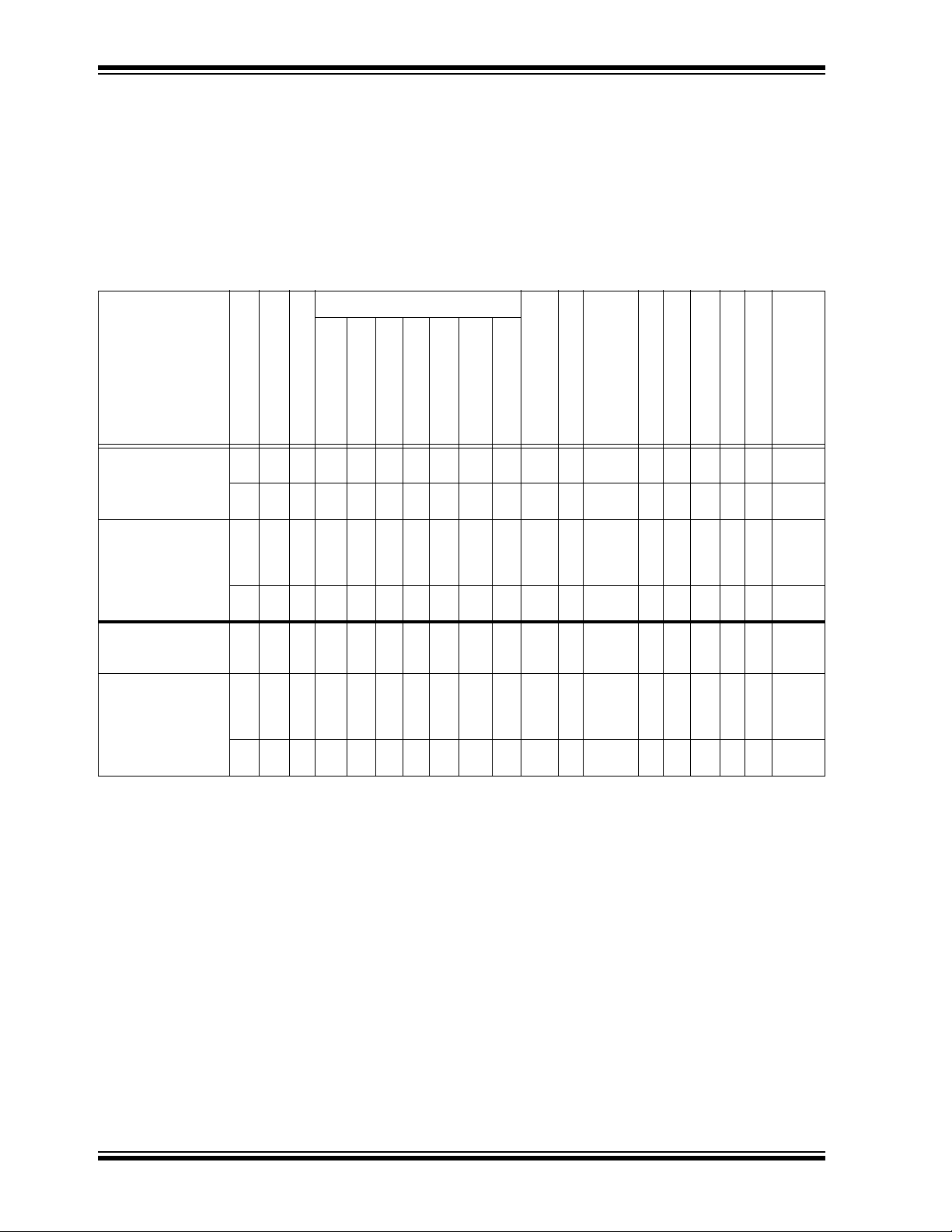
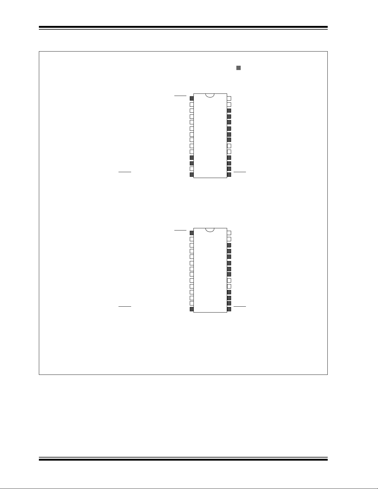
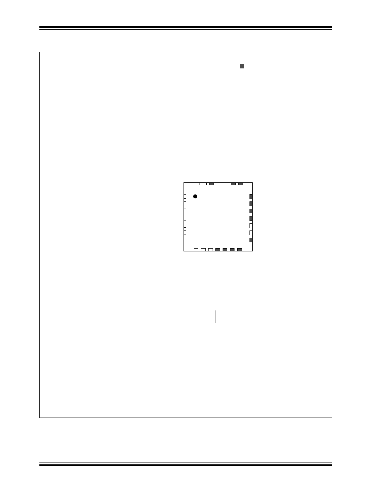
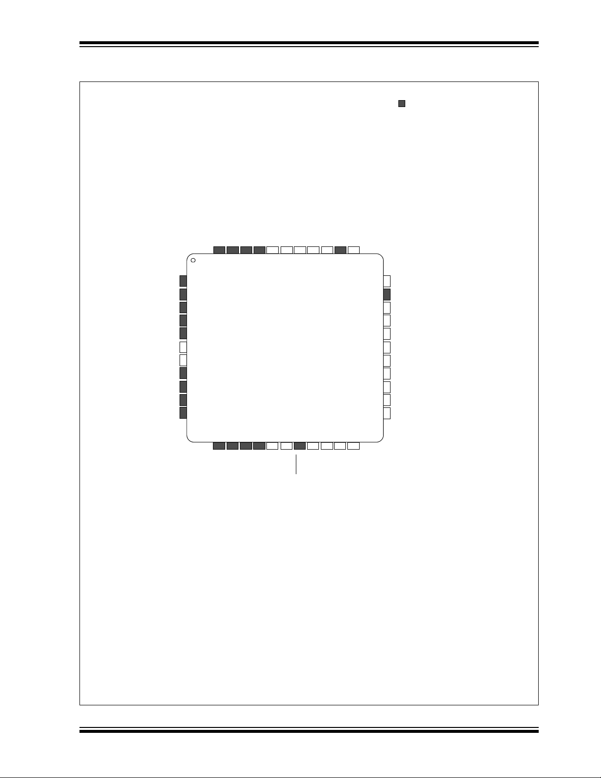
18-Pin PDIP/SOIC
dsPIC33FJ16GP101
MCLR
PGED2/AN0/C3INB/C1INA/CTED1/CN2/RA0
PGEC2/AN1/C3INA/C1INB/CTED2/CN3/RA1
V
DD
VSS
PGED1/AN2/C2INA/C1INC/RP0
(1)
/CN4/RB0
SCK1/INT0/RP7
(1)
/CN23/RB7
PGEC3/SOSCO/T1CK/CN0/RA4
PGED3/SOSCI/RP4
(1)
/CN1/RB4
V
CAP
OSCO/CLKO/CN29/RA3
OSCI/CLKI/CN30/RA2
V
SS
SDA1/SDI1/RP9
(1)
/CN21/RB9
SCL1/SDO1/RP8
(1)
/CN22/RB8
PGEC1/AN3/CV
REFIN/CVREFOUT/C2INB/C1IND/RP1
(1)
/CN5/RB1
1
2
3
4
5
6
7
8
9
18
17
16
15
14
13
12
11
10
RP15
(1)
/CN11/RB15
RTCC/RP14
(1)
/CN12/RB14
Note 1: The RPn pins can be used by any remappable peripheral. See Table 1 for the list of available peripherals.
= Pins are up to 5V tolerant
dsPIC33FJ32GP101
MCLR
PGED2/AN0/C3INB/C1INA/CTED1/CN2/RA0
PGEC2/AN1/C3INA/C1INB/CTED2/CN3/RA1
V
DD
VSS
PGED1/AN2/C2INA/C1INC/RP0
(1)
/CN4/RB0
INT0/RP7
(1)
/CN23/RB7
PGEC3/SOSCO/AN10/T1CK/CN0/RA4
PGED3/SOSCI/AN9/RP4
(1)
/CN1/RB4
V
CAP
OSCO/CLKO/CN29/RA3
OSCI/CLKI/CN30/RA2
V
SS
SDA1/RP9
(1)
/CN21/RB9
SCL1/RP8
(1)
/CN22/RB8
PGEC1/AN3/CV
REFIN/CVREFOUT/C2INB/C1IND/RP1
(1)
/CN5/RB1
1
2
3
4
5
6
7
8
9
18
17
16
15
14
13
12
11
10
RP15
(1)
/CN11/RB15
RTCC/RP14
(1)
/CN12/RB14
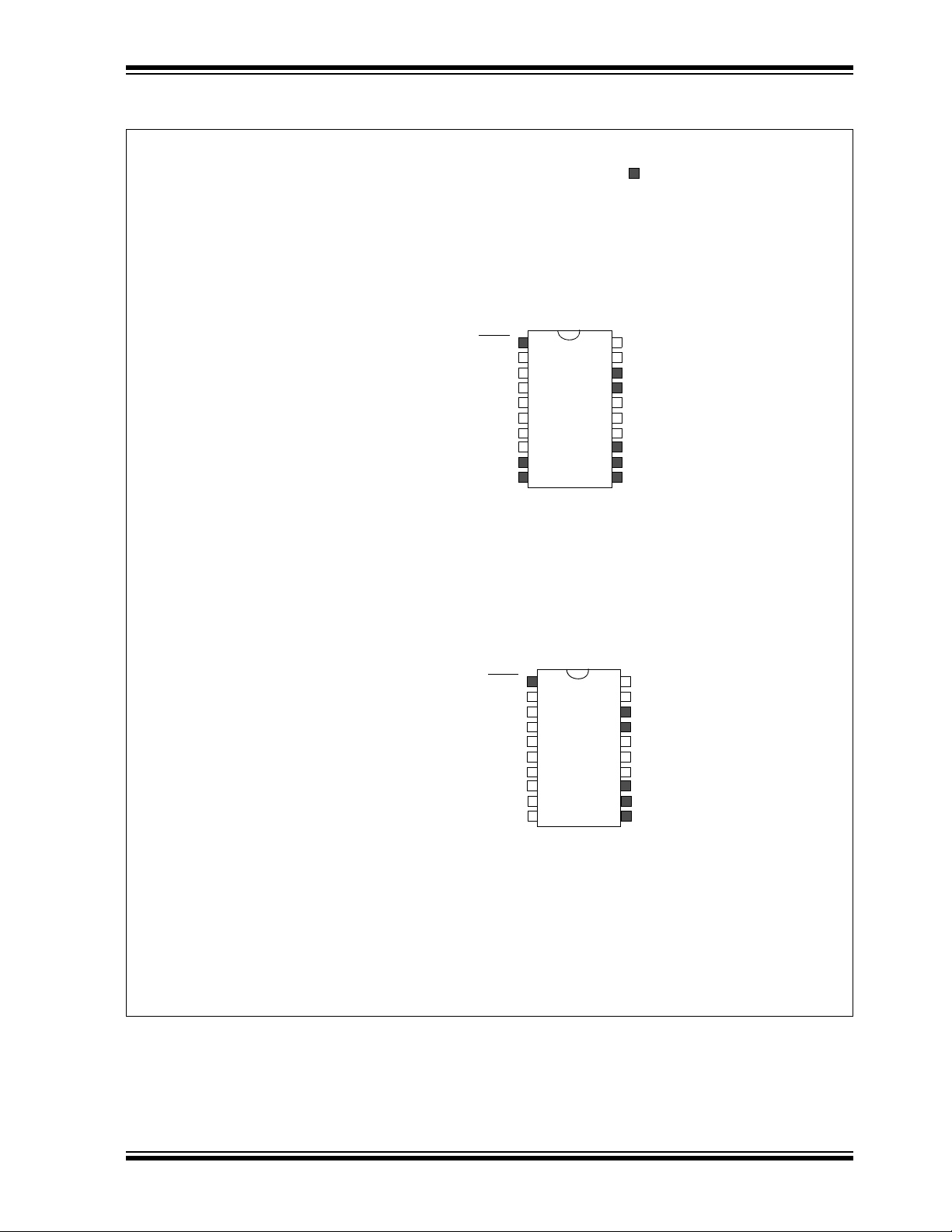
Pin Diagrams
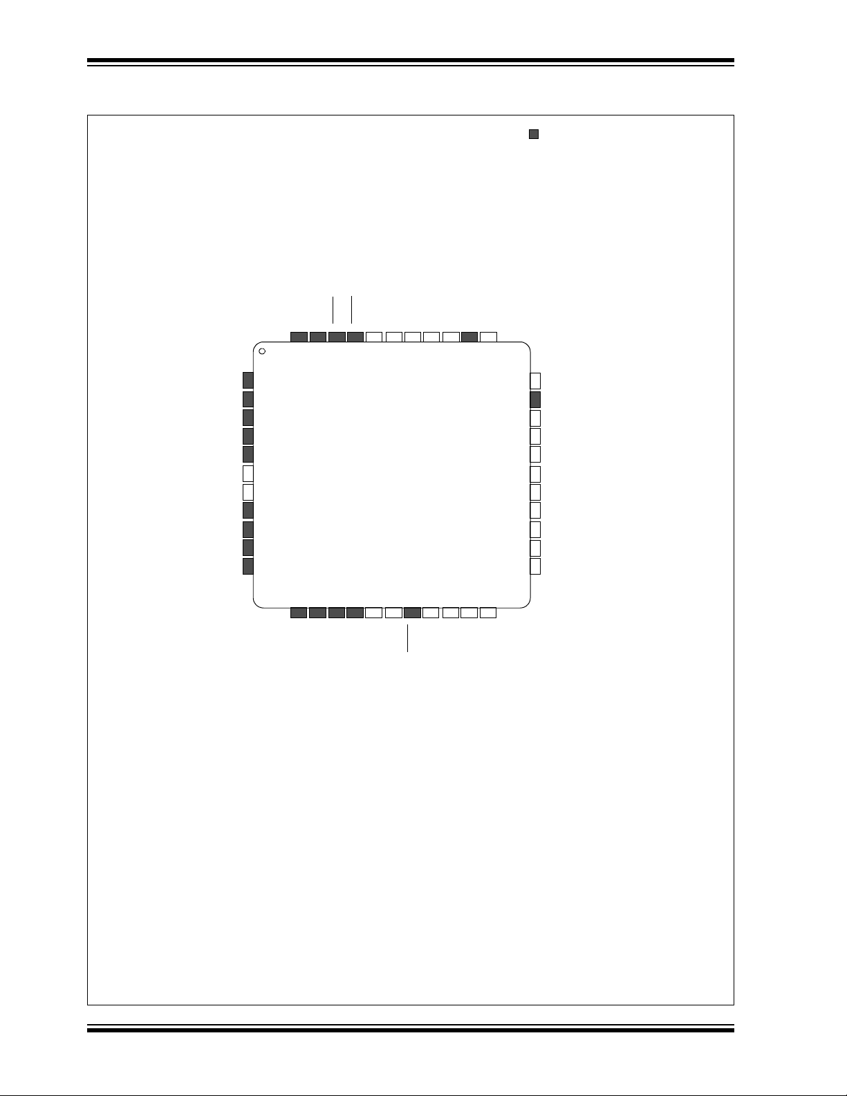
DS70652E-page 4 2011-2012 Microchip Technology Inc.
dsPIC33FJ16(GP/MC)101/102 AND dsPIC33FJ32(GP/MC)101/102/104
dsPIC33FJ16GP101
MCLR
VSS
PGED2/AN0/C3INB/C1INA/CTED1/CN2/RA0
PGEC2/AN1/C3INA/C1INB/CTED2/CN3/RA1
AV
DD
AVSS
PGED1/AN2/C2INA/C1INC/RP0
(1)
/CN4/RB0
SCK1/INT0/RP7
(1)
/CN23/RB7
PGEC3/SOSCO/T1CK/CN0/RA4
PGED3/SOSCI/RP4
(1)
/CN1/RB4
V
CAP
OSCO/CLKO/CN29/RA3
OSCI/CLKI/CN30/RA2
V
SS
SDA1/SDI1/RP9
(1)
/CN21/RB9
SCL1/SDO1/RP8
(1)
/CN22/RB8
PGEC1/AN3/CV
REFIN/CVREFOUT/C2INB/C1IND/RP1
(1)
/CN5/RB1
1
2
3
4
5
6
7
8
9
10
20
19
18
17
16
15
14
13
12
11
RP15
(1)
/CN11/RB15
RTCC/RP14
(1)
/CN12/RB14
V
DD
20-Pin SSOP
Note 1: The RPn pins can be used by any remappable peripheral. See Tab l e 1 for the list of available peripherals.
= Pins are up to 5V tolerant
dsPIC33FJ32GP101
MCLR
VSS
PGED2/AN0/C3INB/C1INA/CTED1/CN2/RA0
PGEC2/AN1/C3INA/C1INB/CTED2/CN3/RA1
AV
DD
AVSS
PGED1/AN2/C2INA/C1INC/RP0
(1)
/CN4/RB0
INT0/RP7
(1)
/CN23/RB7
PGEC3/SOSCO/AN10/T1CK/CN0/RA4
PGED3/SOSCI/AN9/RP4
(1)
/CN1/RB4
V
CAP
OSCO/CLKO/CN29/RA3
OSCI/CLKI/CN30/RA2
V
SS
SDA1/RP9
(1)
/CN21/RB9
SCL1/RP8
(1)
/CN22/RB8
PGEC1/AN3/CV
REFIN/CVREFOUT/C2INB/C1IND/RP1
(1)
/CN5/RB1
1
2
3
4
5
6
7
8
9
10
20
19
18
17
16
15
14
13
12
11
RP15
(1)
/CN11/RB15
RTCC/RP14
(1)
/CN12/RB14
V
DD
Pin Diagrams (Continued)
2011-2012 Microchip Technology Inc. DS70652E-page 5
dsPIC33FJ16(GP/MC)101/102 AND dsPIC33FJ32(GP/MC)101/102/104
dsPIC33FJ16GP102
MCLR
VSS
VDD
PGED2/AN0/C3INB/C1INA/CTED1/CN2/RA0
PGEC2/AN1/C3INA/C1INB/CTED2/CN3/RA1
AV
DD
AVSS
PGED1/AN2/C2INA/C1INC/RP0
(1)
/CN4/RB0
ASCL1/RP6
(1)
/CN24/RB6
PGEC3/SOSCO/T1CK/CN0/RA4
PGED3/SOSCI/RP4
(1)
/CN1/RB4
V
SS
OSCO/CLKO/CN29/RA3
OSCI/CLKI/CN30/RA2
V
CAP
SCK1/INT0/RP7
(1)
/CN23/RB7
SDA1/SDI1/RP9
(1)
/CN21/RB9
SCL1/SDO1/RP8
(1)
/CN22/RB8
AN5/C3IND/C2IND/RP3
(1)
/CN7/RB3
AN4/C3INC/C2INC/RP2
(1)
/CN6/RB2
PGEC1/AN3/CV
REFIN/CVREFOUT/C2INB/C1IND/RP1
(1)
/CN5/RB1
1
2
3
4
5
6
7
8
9
10
11
12
13
14
28
27
26
25
24
23
22
21
20
19
18
17
16
15
RP15
(1)
/CN11/RB15
RTCC/RP14
(1)
/CN12/RB14
RP13
(1)
/CN13/RB13
RP12
(1)
/CN14/RB12
RP10
(1)
/CN16/RB10
RP11
(1)
/CN15/RB11
ASDA1/RP5
(1)
/CN27/RB5
28-Pin SPDIP/SOIC/SSOP
Note 1: The RPn pins can be used by any remappable peripheral. See Table 1 for the list of available peripherals.
= Pins are up to 5V tolerant
dsPIC33FJ32GP102
MCLR
VSS
VDD
PGED2/AN0/C3INB/C1INA/CTED1/CN2/RA0
PGEC2/AN1/C3INA/C1INB/CTED2/CN3/RA1
AV
DD
AVSS
PGED1/AN2/C2INA/C1INC/RP0
(1)
/CN4/RB0
ASCL1/RP6
(1)
/CN24/RB6
PGEC3/SOSCO/AN10/T1CK/CN0/RA4
PGED3/SOSCI/AN9/RP4
(1)
/CN1/RB4
V
SS
OSCO/CLKO/CN29/RA3
OSCI/CLKI/CN30/RA2
V
CAP
INT0/RP7
(1)
/CN23/RB7
SDA1/RP9
(1)
/CN21/RB9
SCL1/RP8
(1)
/CN22/RB8
AN5/C3IND/C2IND/RP3
(1)
/CN7/RB3
AN4/C3INC/C2INC/RP2
(1)
/CN6/RB2
PGEC1/AN3/CV
REFIN/CVREFOUT/C2INB/C1IND/RP1
(1)
/CN5/RB1
1
2
3
4
5
6
7
8
9
10
11
12
13
14
28
27
26
25
24
23
22
21
20
19
18
17
16
15
RP15
(1)
/CN11/RB15
RTCC/RP14
(1)
/CN12/RB14
RP13
(1)
/CN13/RB13
RP12
(1)
/CN14/RB12
RP10
(1)
/CN16/RB10
RP11
(1)
/CN15/RB11
ASDA1/RP5
(1)
/CN27/RB5
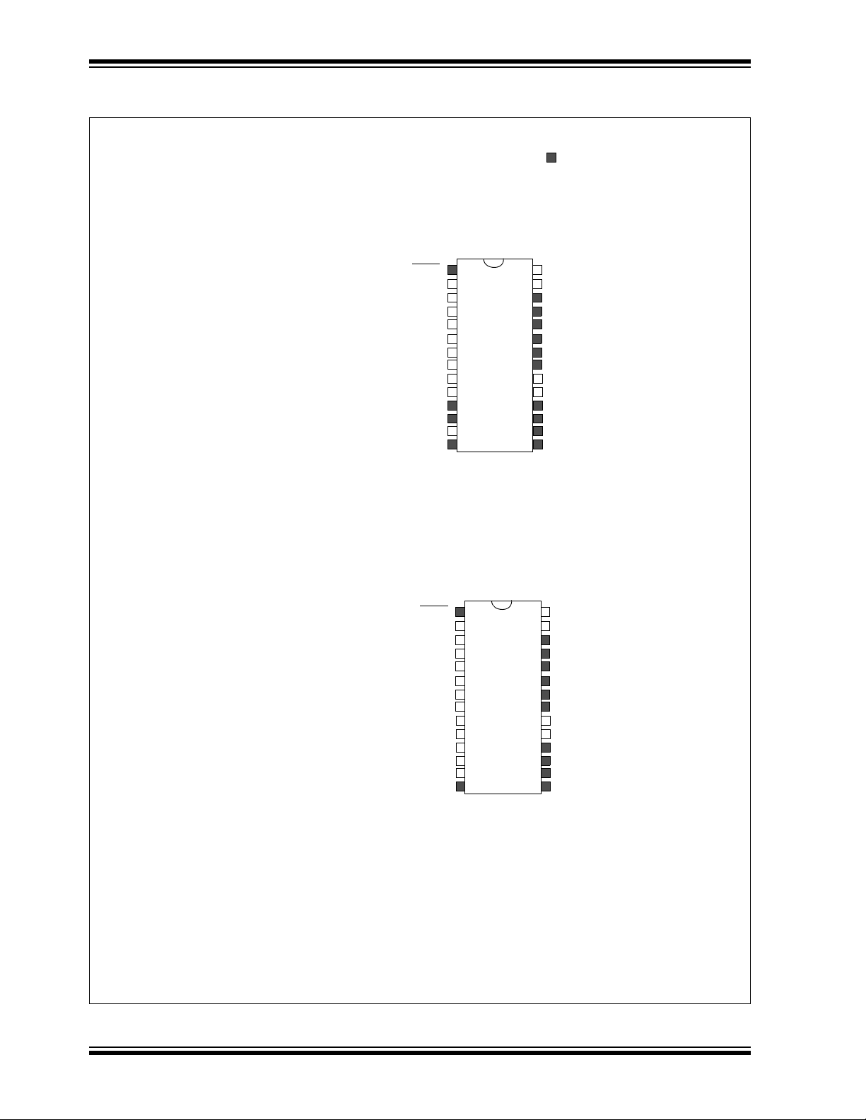
Pin Diagrams (Continued)
DS70652E-page 6 2011-2012 Microchip Technology Inc.
dsPIC33FJ16(GP/MC)101/102 AND dsPIC33FJ32(GP/MC)101/102/104
dsPIC33FJ16MC101
MCLR
VSS
PGED2/AN0/C3INB/C1INA/CTED1/CN2/RA0
PGEC2/AN1/C3INA/C1INB/CTED2/CN3/RA1
V
DD
VSS
PGED1/AN2/C2INA/C1INC/RP0
(1)
/CN4/RB0
FLTA1
(2)
/SCK1/INT0/RP7
(1)
/CN23/RB7
PGEC3/SOSCO/T1CK/CN0/RA4
PGED3/SOSCI/RP4
(1)
/CN1/RB4
PWM1H2/RP12
(1)
/CN14/RB12
OSCO/CLKO/CN29/RA3
OSCI/CLKI/CN30/RA2
V
CAP
SDA1/SDI1/PWM1L3/RP9
(1)
/CN21/RB9
SCL1/SDO1/PWM1H3/RP8
(1)
/CN22/RB8
PGEC1/AN3/CV
REFIN/CVREFOUT/C2INB/C1IND/RP1
(1)
/CN5/RB1
1
2
3
4
5
6
7
8
9
10
20
19
18
17
16
15
14
13
12
11
PWM1L1/RP15
(1)
/CN11/RB15
PWM1H1/RTCC/RP14
(1)
/CN12/RB14
PWM1L2/RP13
(1)
/CN13/RB13
20-Pin PDIP/SOIC/SSOP
Note 1: The RPn pins can be used by any remappable peripheral. See Tab l e 1 for the list of available peripherals.
2: The PWM Fault pins are enabled and asserted during any Reset event. Refer to Section 15.2 “PWM Faults”
for more information on the PWM Faults.
= Pins are up to 5V tolerant
dsPIC33FJ32MC101
MCLR
VSS
PGED2/AN0/C3INB/C1INA/CTED1/CN2/RA0
PGEC2/AN1/C3INA/C1INB/CTED2/CN3/RA1
V
DD
VSS
PGED1/AN2/C2INA/C1INC/RP0
(1)
/CN4/RB0
FLTA1
(2)
/INT0/RP7
(1)
/CN23/RB7
PGEC3/SOSCO/AN10/T1CK/CN0/RA4
PGED3/SOSCI/AN9/RP4
(1)
/CN1/RB4
PWM1H2/RP12
(1)
/CN14/RB12
OSCO/CLKO/CN29/RA3
OSCI/CLKI/CN30/RA2
V
CAP
SDA1/PWM1L3/RP9
(1)
/CN21/RB9
SCL1/PWM1H3/RP8
(1)
/CN22/RB8
PGEC1/AN3/CV
REFIN/CVREFOUT/C2INB/C1IND/RP1
(1)
/CN5/RB1
1
2
3
4
5
6
7
8
9
10
20
19
18
17
16
15
14
13
12
11
PWM1L1/RP15
(1)
/CN11/RB15
PWM1H1/RTCC/RP14
(1)
/CN12/RB14
PWM1L2/RP13
(1)
/CN13/RB13
Pin Diagrams (Continued)
2011-2012 Microchip Technology Inc. DS70652E-page 7
dsPIC33FJ16(GP/MC)101/102 AND dsPIC33FJ32(GP/MC)101/102/104
Note 1: The RPn pins can be used by any remappable peripheral. See Tab l e 1 for the list of available peripherals.
2: The PWM Fault pins are enabled and asserted during any Reset event. Refer to Section 15.2 “PWM Faults”
for more information on the PWM Faults.
dsPIC33FJ16MC102
MCLR
VSS
VDD
PGED2/AN0/C3INB/C1INA/CTED1/CN2/RA0
PGEC2/AN1/C3INA/C1INB/CTED2/CN3/RA1
AV
DD
AVSS
PGED1/AN2/C2INA/C1INC/RP0
(1)
/CN4/RB0
FLTA1
(2)
/ASCL1/RP6
(1)
/CN24/RB6
PGEC3/SOSCO/T1CK/CN0/RA4
PGED3/SOSCI/RP4
(1)
/CN1/RB4
V
SS
OSCO/CLKO/CN29/RA3
OSCI/CLKI/CN30/RA2
V
CAP
SCK1/INT0/RP7
(1)
/CN23/RB7
SDA1/SDI1/RP9
(1)
/CN21/RB9
SCL1/SDO1/RP8
(1)
/CN22/RB8
AN5/C3IND/C2IND/RP3
(1)
/CN7/RB3
AN4/C3INC/C2INC/RP2
(1)
/CN6/RB2
PGEC1/AN3/CV
REFIN/CVREFOUT/C2INB/C1IND/RP1
(1)
/CN5/RB1
1
2
3
4
5
6
7
8
9
10
11
12
13
14
28
27
26
25
24
23
22
21
20
19
18
17
16
15
PWM1L1/RP15
(1)
/CN11/RB15
PWM1H1/RTCC/RP14
(1)
/CN12/RB14
PWM1L2/RP13
(1)
/CN13/RB13
PWM1H2/RP12
(1)
/CN14/RB12
PWM1H3/RP10
(1)
/CN16/RB10
PWM1L3/RP11
(1)
/CN15/RB11
FLTB1
(2)
/ASDA1/RP5
(1)
/CN27/RB5
28-Pin SPDIP/SOIC/SSOP
= Pins are up to 5V tolerant
dsPIC33FJ32MC102
MCLR
VSS
VDD
PGED2/AN0/C3INB/C1INA/CTED1/CN2/RA0
PGEC2/AN1/C3INA/C1INB/CTED2/CN3/RA1
AV
DD
AVSS
PGED1/AN2/C2INA/C1INC/RP0
(1)
/CN4/RB0
FLTA1
(2)
/ASCL1/RP6
(1)
/CN24/RB6
PGEC3/SOSCO/AN10/T1CK/CN0/RA4
PGED3/SOSCI/AN9/RP4
(1)
/CN1/RB4
V
SS
OSCO/CLKO/CN29/RA3
OSCI/CLKI/CN30/RA2
V
CAP
INT0/RP7
(1)
/CN23/RB7
SDA1/RP9
(1)
/CN21/RB9
SCL1/RP8
(1)
/CN22/RB8
AN5/C3IND/C2IND/RP3
(1)
/CN7/RB3
AN4/C3INC/C2INC/RP2
(1)
/CN6/RB2
PGEC1/AN3/CV
REFIN/CVREFOUT/C2INB/C1IND/RP1
(1)
/CN5/RB1
1
2
3
4
5
6
7
8
9
10
11
12
13
14
28
27
26
25
24
23
22
21
20
19
18
17
16
15
PWM1L1/RP15
(1)
/CN11/RB15
PWM1H1/RTCC/RP14
(1)
/CN12/RB14
PWM1L2/RP13
(1)
/CN13/RB13
PWM1H2/RP12
(1)
/CN14/RB12
PWM1H3/RP10
(1)
/CN16/RB10
PWM1L3/RP11
(1)
/CN15/RB11
FLTB1
(2)
/ASDA1/RP5
(1)
/CN27/RB5
Pin Diagrams (Continued)
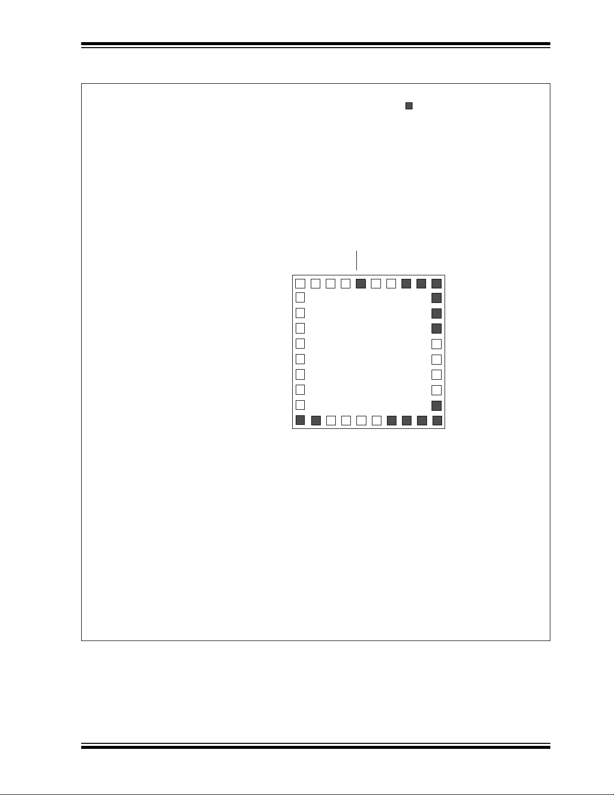
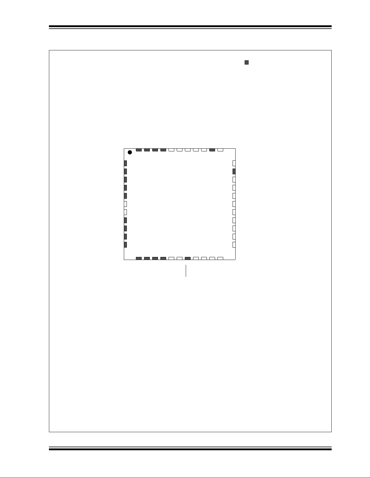
DS70652E-page 8 2011-2012 Microchip Technology Inc.
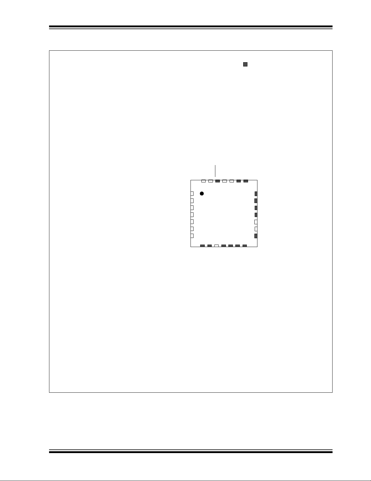
dsPIC33FJ16(GP/MC)101/102 AND dsPIC33FJ32(GP/MC)101/102/104
28-Pin QFN
(2)
Note 1: The RPn pins can be used by any remappable peripheral. See Table 1 for the list of available peripherals.
2: The metal pad at the bottom of the device is not connected to any pins and is recommended to be connected
to V
SS externally.
= Pins are up to 5V tolerant
10 11
2
3
6
1
18
19
20
21
22
12 13 14
15
8
7
16
17
232425262728
9
dsPIC33FJ16GP102
5
4
MCLR
PGED2/AN0/C3INB/C1INA/CTED1/CN2/RA0
PGEC2/AN1/C3INA/C1INB/CTED2/CN3/RA1
VSS
VCAP
SDA1/SDI1/RP9
(1)
/CN21/RB9
RP13
(1)
/CN13/RB13
RP12
(1)
/CN14/RB12
RP10
(1)
/CN16/RB10
RP11
(1)
/CN15/RB11
V
SS
PGED1/AN2/C2INA/C1INC/RP0
(1)
/CN4/RB0
OSCO/CLKO/CN29/RA3
OSCI/CLKI/CN30/RA2
AN5/C3IND/C2IND/RP3
(1)
/CN7/RB3
AN4/C3INC/C2INC/RP2
(1)
/CN6/RB2
PGEC1/AN3/CV
REFIN/CVREFOUT/C2INB/C1IND/RP1
(1)
/CN5/RB1
VDD
PGEC3/SOSCO/T1CK/CN0/RA4
ASDA1/RP5
(1)
/CN27/RB5
PGED3/SOSCI/RP4
(1)
/CN1/RB4
ASCL1/RP6
(1)
/CN24/RB6
SCK1/INT0/RP7
(1)
/CN23/RB7
SCL1/SDO1/RP8
(1)
/CN22/RB8
AV
DD
AVSS
RP15
(1)
/CN11/RB15
RTCC/RP14
(1)
/CN12/RB14
Pin Diagrams (Continued)
2011-2012 Microchip Technology Inc. DS70652E-page 9
dsPIC33FJ16(GP/MC)101/102 AND dsPIC33FJ32(GP/MC)101/102/104
28-Pin QFN
(2)
Note 1: The RPn pins can be used by any remappable peripheral. See Tab l e 1 for the list of available peripherals.
2: The metal pad at the bottom of the device is not connected to any pins and is recommended to be connected
to V
SS externally.
= Pins are up to 5V tolerant
10 11
2
3
6
1
18
19
20
21
22
12 13 14
15
8
7
16
17
232425262728
9
dsPIC33FJ32GP102
5
4
MCLR
PGED2/AN0/C3INB/C1INA/CTED1/CN2/RA0
PGEC2/AN1/C3INA/C1INB/CTED2/CN3/RA1
VSS
VCAP
SDA1/RP9
(1)
/CN21/RB9
RP13
(1)
/CN13/RB13
RP12
(1)
/CN14/RB12
RP10
(1)
/CN16/RB10
RP11
(1)
/CN15/RB11
V
SS
PGED1/AN2/C2INA/C1INC/RP0
(1)
/CN4/RB0
OSCO/CLKO/CN29/RA3
OSCI/CLKI/CN30/RA2
AN5/C3IND/C2IND/RP3
(1)
/CN7/RB3
AN4/C3INC/C2INC/RP2
(1)
/CN6/RB2
PGEC1/AN3/CV
REFIN/CVREFOUT/C2INB/C1IND/RP1
(1)
/CN5/RB1
VDD
PGEC3/SOSCOAN10//T1CK/CN0/RA4
ASDA1/RP5
(1)
/CN27/RB5
PGED3/SOSCI/AN9/RP4
(1)
/CN1/RB4
ASCL1/RP6
(1)
/CN24/RB6
INT0/RP7
(1)
/CN23/RB7
SCL1/RP8
(1)
/CN22/RB8
AV
DD
AVSS
RP15
(1)
/CN11/RB15
RTCC/RP14
(1)
/CN12/RB14
Pin Diagrams (Continued)
DS70652E-page 10 2011-2012 Microchip Technology Inc.
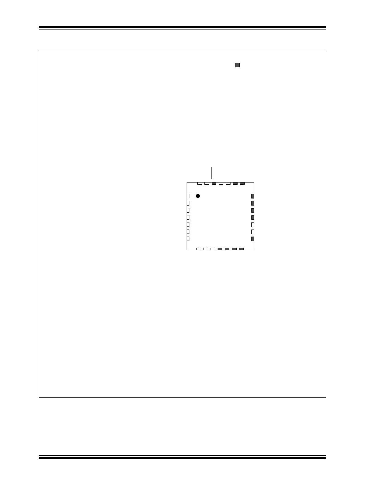
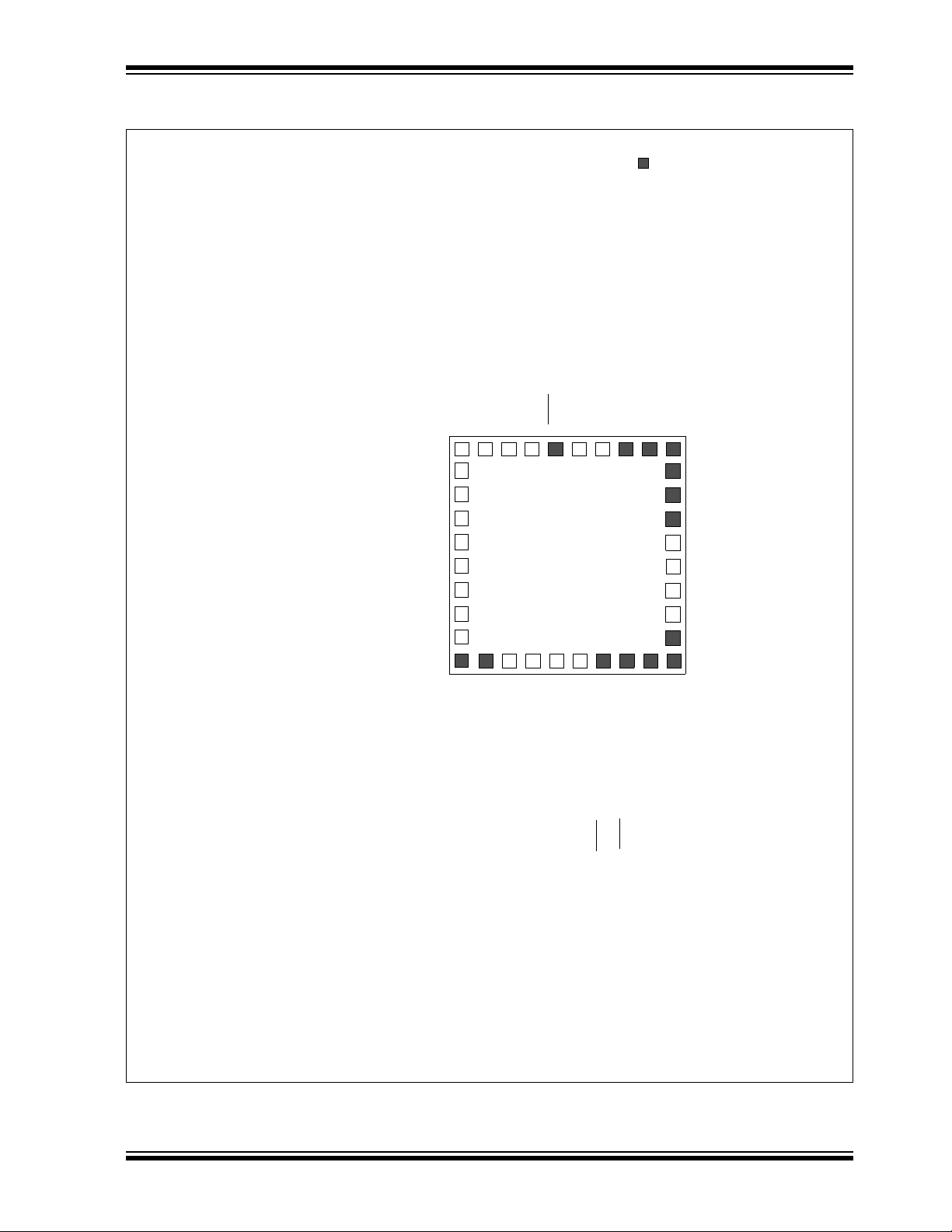
dsPIC33FJ16(GP/MC)101/102 AND dsPIC33FJ32(GP/MC)101/102/104
28-Pin QFN
(2)
Note 1: The RPn pins can be used by any remappable peripheral. See Tab l e 1 for the list of available peripherals.
2: The metal pad at the bottom of the device is not connected to any pins and is recommended to be connected
to V
SS externally.
3: The PWM Fault pins are enabled and asserted during any Reset event. Refer to Section 15.2 “PWM Faults”
for more information on the PWM Faults.
10 11
2
3
6
1
18
19
20
21
22
12 13 14
15
8
7
16
17
232425262728
9
dsPIC33FJ16MC102
5
4
MCLR
PGED2/AN0/C3INB/C1INA/CTED1/CN2/RA0
PGEC2/AN1/C3INA/C1INB/CTED2/CN3/RA1
VSS
VCAP
SDA1/SDI1/RP9
(1)
/CN21/RB9
PWM1L2/RP13
(1)
/CN13/RB13
PWM1H2/RP12
(1)
/CN14/RB12
PWM1H3/RP10
(1)
/CN16/RB10
PWM1L3/RP11
(1)
/CN15/RB11
V
SS
PGED1/AN2/C2INA/C1INC/RP0
(1)
/CN4/RB0
OSCO/CLKO/CN29/RA3
OSCI/CLKI/CN30/RA2
AN5/C3IND/C2IND/RP3
(1)
/CN7/RB3
AN4/C3INC/C2INC/RP2
(1)
/CN6/RB2
PGEC1/AN3/CV
REFIN/CVREFOUT/C2INB/C1IND/RP1
(1)
/CN5/RB1
VDD
PGEC3/SOSCO/T1CK/CN0/RA4
FLTB1
(3)
/ASDA1/RP5
(1)
/CN27/RB5
PGED3/SOSCI/RP4
(1)
/CN1/RB4
FLTA1
(3)
/ASCL1/RP6
(1)
/CN24/RB6
SCK1/INT0/RP7
(1)
/CN23/RB7
SCL1/SDO1/RP8
(1)
/CN22/RB8
AV
DD
AVSS
PWM1L1/RP15
(1)
/CN11/RB15
PWM1H1/RTCC/RP14
(1)
/CN12/RB14
= Pins are up to 5V tolerant
Pin Diagrams (Continued)
2011-2012 Microchip Technology Inc. DS70652E-page 11
dsPIC33FJ16(GP/MC)101/102 AND dsPIC33FJ32(GP/MC)101/102/104
28-Pin QFN
(2)
Note 1: The RPn pins can be used by any remappable peripheral. See Table 1 for the list of available peripherals.
2: The metal pad at the bottom of the device is not connected to any pins and is recommended to be connected
to V
SS externally.
3: The PWM Fault pins are enabled and asserted during any Reset event. Refer to Section 15.2 “PWM
Faults” for more information on the PWM Faults.
10 11
2
3
6
1
18
19
20
21
22
12 13 14
15
8
7
16
17
232425262728
9
dsPIC33FJ32MC102
5
4
MCLR
PGED2/AN0/C3INB/C1INA/CTED1/CN2/RA0
PGEC2/AN1/C3INA/C1INB/CTED2/CN3/RA1
VSS
VCAP
SDA1/RP9
(1)
/CN21/RB9
PWM1L2/RP13
(1)
/CN13/RB13
PWM1H2/RP12
(1)
/CN14/RB12
PWM1H3/RP10
(1)
/CN16/RB10
PWM1L3/RP11
(1)
/CN15/RB11
V
SS
PGED1/AN2/C2INA/C1INC/RP0
(1)
/CN4/RB0
OSCO/CLKO/CN29/RA3
OSCI/CLKI/CN30/RA2
AN5/C3IND/C2IND/RP3
(1)
/CN7/RB3
AN4/C3INC/C2INC/RP2
(1)
/CN6/RB2
PGEC1/AN3/CV
REFIN/CVREFOUT/C2INB/C1IND/RP1
(1)
/CN5/RB1
VDD
PGEC3/SOSCO/AN10/T1CK/CN0/RA4
FLTB1
(3)
/ASDA1/RP5
(1)
/CN27/RB5
PGED3/SOSCI/AN9/RP4
(1)
/CN1/RB4
FLTA1
(3)
/ASCL1/RP6
(1)
/CN24/RB6
INT0/RP7
(1)
/CN23/RB7
SCL1/RP8
(1)
/CN22/RB8
AV
DD
AVSS
PWM1L1/RP15
(1)
/CN11/RB15
PWM1H1/RTCC/RP14
(1)
/CN12/RB14
= Pins are up to 5V tolerant
Pin Diagrams (Continued)
DS70652E-page 12 2011-2012 Microchip Technology Inc.
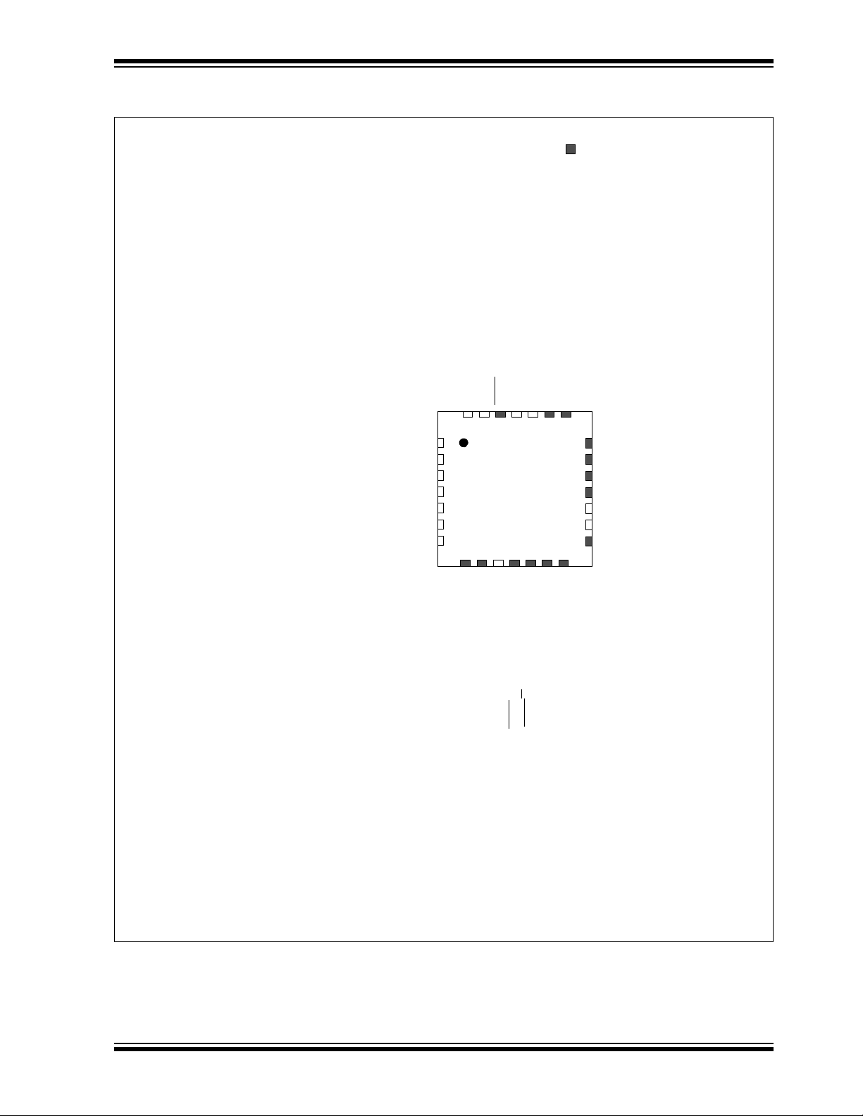
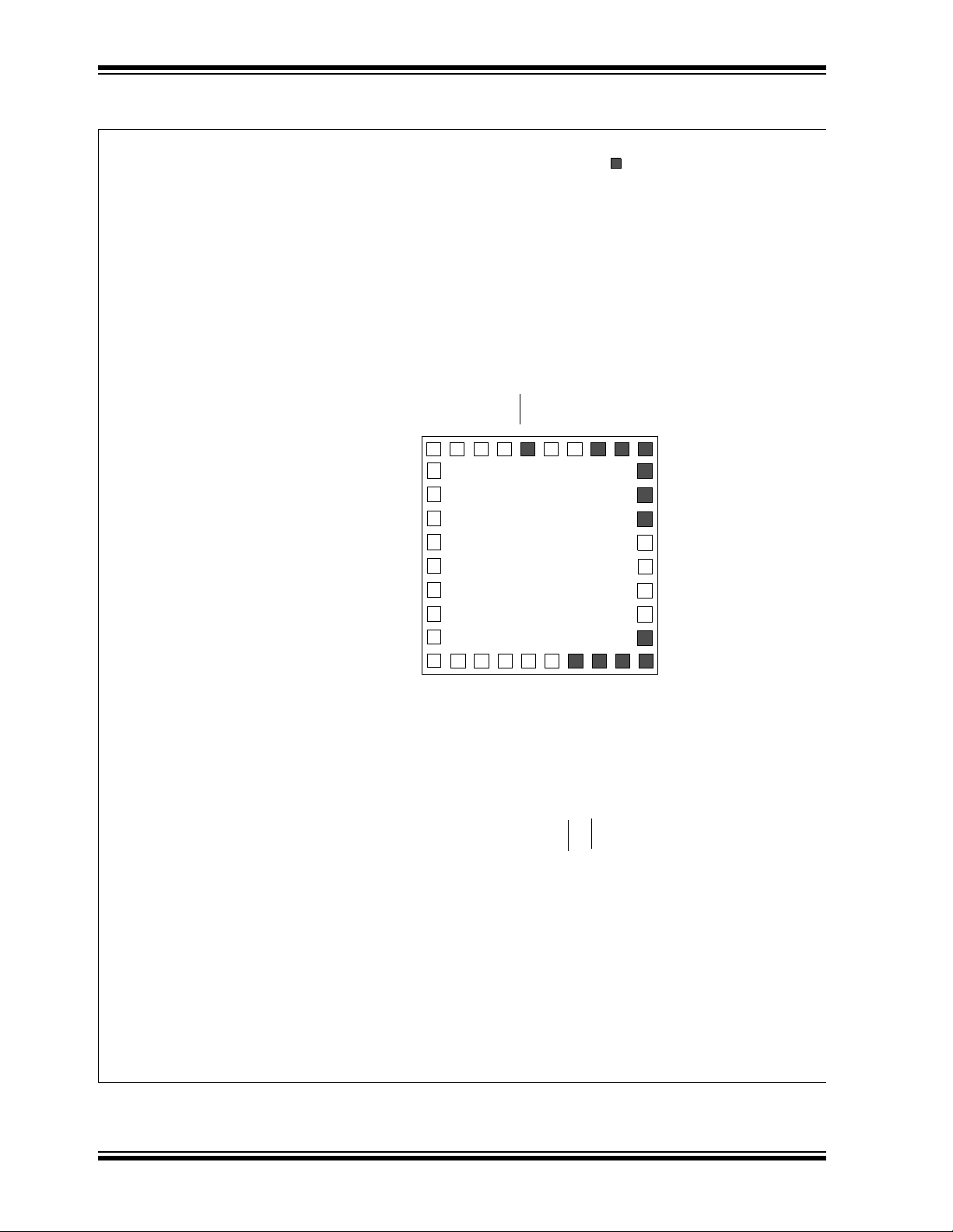
dsPIC33FJ16(GP/MC)101/102 AND dsPIC33FJ32(GP/MC)101/102/104
36-Pin VTLA
(2)
Note 1: The RPn pins can be used by any remappable peripheral. See Table 1 for the list of available peripherals.
2: The metal pad at the bottom of the device is not connected to any pins and is recommended to be connected
to V
SS externally.
1
dsPIC33FJ16GP102
10
33 32 31 30 29 28
2
3
4
5
6
24
23
22
21
20
19
11 12 13 14 15
N/C
PGED2/AN0/C3INB/C1INA/CTED1/CN2/RA0
PGEC2/AN1/C3INA/C1INB/CTED2/CN3/RA1
MCLR
AVDD
RP15
(1)
/CN11/RB15
RTCC/RP14
(1)
/CN12/RB14
AV
SS
N/C
N/C
V
SS
SDA1/SDI1/RP9
(1)
/CN21/RB9
RP13
(1)
/CN13/RB13
RP12
(1)
/CN14/RB12
RP10
(1)
/CN16/RB10
RP11
(1)
/CN15/RB11
V
DD
VCAP
VDD
PGED1/AN2/C2INA/C1INC/RP0
(1)
/CN4/RB0
PGED3/SOSCI/RP4
(1)
/CN1/RB4
OSCO/CLKO/CN29/RA3
AN5/C3IND/C2IND/RP3
(1)
/CN7/RB3
AN4/C3INC/C2INC/RP2
(1)
/CN6/RB2
PGEC1/AN3/CV
REFIN/CVREFOUT/C2INB/C1IND/RP1
(1)
/CN5/RB1
V
SS
OSCI/CLKI/CN30/RA2
N/C (Vss)
N/C
ASDA1/RP5
(1)
/CN27/RB5
PGEC3/SOSCO/T1CK/CN0/RA4
ASCL1/RP6
(1)
/CN24/RB6
SCK1/INT0/RP7
(1)
/CN23/RB7
SCL1/SDO1/RP8
(1)
/CN22/RB8
V
DD
N/C (VDD)
7
8
9
34
35
36
16
17
18
27
26
25
= Pins are up to 5V tolerant
Pin Diagrams (Continued)
2011-2012 Microchip Technology Inc. DS70652E-page 13

dsPIC33FJ16(GP/MC)101/102 AND dsPIC33FJ32(GP/MC)101/102/104
36-Pin VTLA
(2)
Note 1: The RPn pins can be used by any remappable peripheral. See Tab l e 1 for the list of available peripherals.
2: The metal pad at the bottom of the device is not connected to any pins and is recommended to be connected
to V
SS externally.
1
dsPIC33FJ32GP102
10
33 32 31 30 29 28
2
3
4
5
6
24
23
22
21
20
19
11 12 13 14 15
N/C
PGED2/AN0/C3INB/C1INA/CTED1/CN2/RA0
PGEC2/AN1/C3INA/C1INB/CTED2/CN3/RA1
MCLR
AVDD
RP15
(1)
/CN11/RB15
RTCC/RP14
(1)
/CN12/RB14
AV
SS
N/C
N/C
V
SS
SDA1/RP9
(1)
/CN21/RB9
RP13
(1)
/CN13/RB13
RP12
(1)
/CN14/RB12
RP10
(1)
/CN16/RB10
RP11
(1)
/CN15/RB11
V
DD
VCAP
VDD
PGED1/AN2/C2INA/C1INC/RP0
(1)
/CN4/RB0
PGED3/SOSCI/AN9/RP4
(1)
/CN1/RB4
OSCO/CLKO/CN29/RA3
AN5/C3IND/C2IND/RP3
(1)
/CN7/RB3
AN4/C3INC/C2INC/RP2
(1)
/CN6/RB2
PGEC1/AN3/CV
REFIN/CVREFOUT/C2INB/C1IND/RP1
(1)
/CN5/RB1
V
SS
OSCI/CLKI/CN30/RA2
N/C (Vss)
N/C
ASDA1/RP5
(1)
/CN27/RB5
PGEC3/SOSCO/AN10/T1CK/CN0/RA4
ASCL1/RP6
(1)
/CN24/RB6
INT0/RP7
(1)
/CN23/RB7
SCL1/RP8
(1)
/CN22/RB8
V
DD
N/C (VDD)
7
8
9
34
35
36
16
17
18
27
26
25
= Pins are up to 5V tolerant
Pin Diagrams (Continued)
DS70652E-page 14 2011-2012 Microchip Technology Inc.
dsPIC33FJ16(GP/MC)101/102 AND dsPIC33FJ32(GP/MC)101/102/104
36-Pin VTLA
(2)
Note 1: The RPn pins can be used by any remappable peripheral. See Tab l e 1 for the list of available peripherals.
2: The metal pad at the bottom of the device is not connected to any pins and is recommended to be connected
to V
SS externally.
3: The PWM Fault pins are enabled and asserted during any Reset event. Refer to Section 15.2 “PWM Faults”
for more information on the PWM Faults.
N/C
PGED2/AN0/C3INB/C1INA/CTED1/CN2/RA0
PGEC2/AN1/C3INA/C1INB/CTED2/CN3/RA1
MCLR
AVDD
PWM1L1/RP15
(1)
/CN11/RB15
AV
SS
N/C
N/C
V
SS
SDA1/SDI1/RP9
(1)
/CN21/RB9
PWM1L2/RP13
(1)
/CN13/RB13
PWM1H2/RP12
(1)
/CN14/RB12
PWM1H3/RP10
(1)
/CN16/RB10
PWM1L3/RP11
(1)
/CN15/RB11
V
DD
VCAP
VDD
PGED1/AN2/C2INA/C1INC/RP0
(1)
/CN4/RB0
PGED3/SOSCI/RP4
(1)
/CN1/RB4
OSCO/CLKO/CN29/RA3
AN5/C3IND/C2IND/RP3
(1)
/CN7/RB3
AN4/C3INC/C2INC/RP2
(1)
/CN6/RB2
PGEC1/AN3/CV
REFIN/CVREFOUT/C2INB/C1IND/RP1
(1)
/CN5/RB1
V
SS
OSCI/CLKI/CN30/RA2
N/C (Vss)
N/C
FLTB1
(3)
/ASDA1/RP5
(1)
/CN27/RB5
PGEC3/SOSCO/T1CK/CN0/RA4
FLTA1
(3)
/ASCL1/RP6
(1)
/CN24/RB6
SCK1/INT0/RP7
(1)
/CN23/RB7
SCL1/SDO1/RP8
(1)
/CN22/RB8
V
DD
N/C (VDD)
dsPIC33FJ16MC102
= Pins are up to 5V tolerant
1
10
33 32 31 30 29 28
2
3
4
5
6
24
23
22
21
20
19
11 12 13 14 15
7
8
9
34
35
36
16
17
18
27
26
25
PWM1H1/RTCC/RP14
(1)
/CN12/RB14
Pin Diagrams (Continued)
2011-2012 Microchip Technology Inc. DS70652E-page 15
dsPIC33FJ16(GP/MC)101/102 AND dsPIC33FJ32(GP/MC)101/102/104
36-Pin VTLA
(2)
Note 1: The RPn pins can be used by any remappable peripheral. See Table 1 for the list of available peripherals.
2: The metal pad at the bottom of the device is not connected to any pins and is recommended to be connected
to V
SS externally.
3: The PWM Fault pins are enabled and asserted during any Reset event. Refer to Section 15.2 “PWM Faults”
for more information on the PWM Faults.
N/C
PGED2/AN0/C3INB/C1INA/CTED1/CN2/RA0
PGEC2/AN1/C3INA/C1INB/CTED2/CN3/RA1
MCLR
AVDD
PWM1L1/RP15
(1)
/CN11/RB15
PWM1H1/RTCC/RP14
(1)
/CN12/RB14
AV
SS
N/C
N/C
V
SS
SDA1/RP9
(1)
/CN21/RB9
PWM1L2/RP13
(1)
/CN13/RB13
PWM1H2/RP12
(1)
/CN14/RB12
PWM1H3/RP10
(1)
/CN16/RB10
PWM1L3/RP11
(1)
/CN15/RB11
V
DD
VCAP
VDD
PGED1/AN2/C2INA/C1INC/RP0
(1)
/CN4/RB0
PGED3/SOSCI/AN9/RP4
(1)
/CN1/RB4
OSCO/CLKO/CN29/RA3
AN5/C3IND/C2IND/RP3
(1)
/CN7/RB3
AN4/C3INC/C2INC/RP2
(1)
/CN6/RB2
PGEC1/AN3/CV
REFIN/CVREFOUT/C2INB/C1IND/RP1
(1)
/CN5/RB1
V
SS
OSCI/CLKI/CN30/RA2
N/C (Vss)
N/C
FLTB1
(3)
/ASDA1/RP5
(1)
/CN27/RB5
PGEC3/SOSCO/AN10/T1CK/CN0/RA4
FLTA1
(3)
/ASCL1/RP6
(1)
/CN24/RB6
INT0/RP7
(1)
/CN23/RB7
SCL1/RP8
(1)
/CN22/RB8
V
DD
N/C (VDD)
dsPIC33FJ32MC102
= Pins are up to 5V tolerant
1
10
33 32 31 30 29 28
2
3
4
5
6
24
23
22
21
20
19
11 12 13 14 15
7
8
9
34
35
36
16
17
18
27
26
25
Pin Diagrams (Continued)
DS70652E-page 16 2011-2012 Microchip Technology Inc.
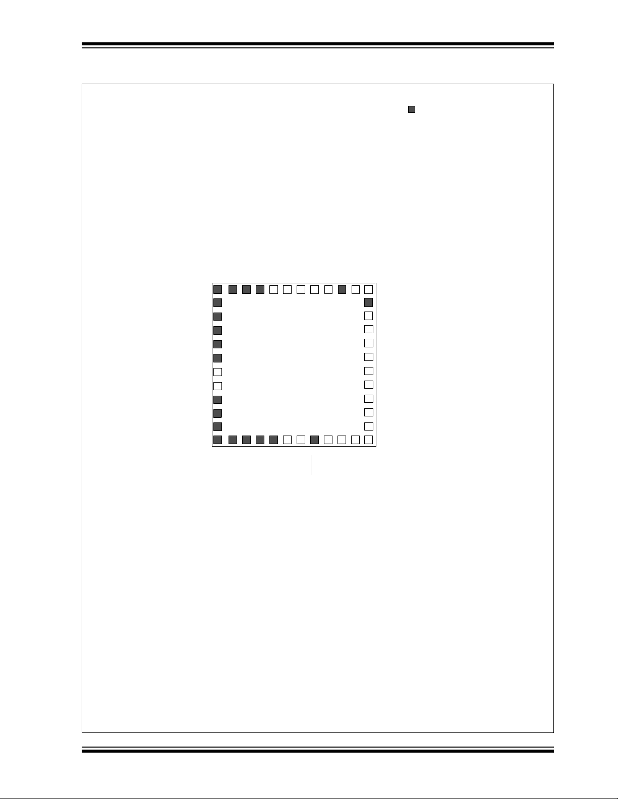
dsPIC33FJ16(GP/MC)101/102 AND dsPIC33FJ32(GP/MC)101/102/104
44 43 42 41 40 39 38 37 36 35 34
133
232
331
430
529
628
727
826
925
10 24
11 23
12 13 14 15 16 17 18 19 20 21 22
44-Pin TQFP
= Pins are up to 5V tolerant
SCL1/RP8
(1)
/CN22/RB8RA10
RA7
RTCC/RP14
(1)
/CN12/RB14
RP15
(1)
/CN11/RB15
A
VSS
AVDD
MCLR
PGED2/AN0/C3INB/C1INA/CTED1/CN2/RA0
PGEC2/AN1/C3INA/C1INB/CTED2/CN3/RA1
PGED1/AN2/C2INA/C1INC/RP0
(1)
/CN4/RB0
PGEC1/AN3/CV
REFIN/CVREFOUT/C2INB/C1IND/RP1
(1)
/CN5/RB1
INT0/RP7
(1)
/CN23/RB7
ASCL1/RP6
(1)
/CN24/RB6
ASDA1/RP5
(1)
/CN27/RB5
VDDVSS
AN15/RP21
(1)
/CN26/RC5
AN12/RP20
(1)
/CN25/RC4
AN11/RP19
(1)
/CN28/RC3
RA9
PGEC3/SOSCO/AN10/T1CK/CN0/RA4
dsPIC33FJ32GP104
RP13
(1)
/CN13/RB13
RP12
(1)
/CN14/RB12
RP11
(1)
/CN15/RB11
RP10/CN16/RB10
V
CAP
VSS
RP25
(1)
/CN19/RC9
RP24
(1)
/CN20/RC8
RP23
(1)
/CN17/RC7
SDA1/RP9
(1)
/CN21/RB9
RP22
(1)
/CN18/RC6
PEGED3/SOSCI/AN9/RP4
(1)
/CN1/RB4
RA8
OSC2/CLK0/CN29/RA3
OSC1/CLKI/CN30/RA2
V
SS
VDD
AN8/RP18
(1)
/CN10/RC2
AN7/RP17
(1)
/CN9/RC1
AN6/RP16
(1)
/CN8/RC0
AN5/C3IND/C2IND/RP3
(1)
/CN7/RB3
AN4/C3INC/C2INC/RP2
(1)
/CN6/RB2
Note 1: The RPn pins can be used by any remappable peripheral. See Table 1 for the list of available peripherals.
Pin Diagrams (Continued)
2011-2012 Microchip Technology Inc. DS70652E-page 17
dsPIC33FJ16(GP/MC)101/102 AND dsPIC33FJ32(GP/MC)101/102/104
44-Pin TQFP
= Pins are up to 5V tolerant
44 43 42 41 40 39 38 37 36 35 34
133
232
331
430
529
628
727
826
925
10 24
11 23
12 13 14 15 16 17 18 19 20 21 22
SCL1/RP8
(1)
/CN22/RB8RA10
RA7
PWM1H1/RTCC/RP14
(1)
/CN12/RB14
PWM1L1/RP15
(1)
/CN11/RB15
A
VSS
AVDD
MCLR
PGED2/AN0/C3INB/C1INA/CTED1/CN2/RA0
PGEC2/AN1/C3INA/C1INB/CTED2/CN3/RA1
PGED1/AN2/C2INA/C1INC/RP0
(1)
/CN4/RB0
PGEC1/AN3/CV
REFIN/CVREFOUT/C2INB/C1IND/RP1
(1)
/CN5/RB1
INT0/RP7
(1)
/CN23/RB7
FLTA1
(2)
/ASCL1/RP6
(1)
/CN24/RB6
FLTB1
(2)
/ASDA1/RP5
(1)
/CN27/RB5
V
DD
VSS
AN15/RP21
(1)
/CN26/RC5
AN12/RP20
(1)
/CN25/RC4
AN11/RP19
(1)
/CN28/RC3
RA9
PGEC3/SOSCO/AN10/T1CK/CN0/RA4
dsPIC33FJ32MC104
PWM1L2/RP13
(1)
/CN13/RB13
PWM1H2/RP12
(1)
/CN14/RB12
PWM1L3/RP11
(1)
/CN15/RB11
PWM1H3/RP10
(1)
/CN16/RB10
V
CAP
VSS
RP25
(1)
/CN19/RC9
RP24
(1)
/CN20/RC8
RP23
(1)
/CN17/RC7
SDA1/RP9
(1)
/CN21/RB9
RP22
(1)
/CN18/RC6
PEGED3/SOSCI/AN9/RP4
(1)
/CN1/RB4
RA8
OSC2/CLK0/CN29/RA3
OSC1/CLKI/CN30/RA2
V
SS
VDD
AN8/RP18
(1)
/CN10/RC2
AN7/RP17
(1)
/CN9/RC1
AN6/RP16
(1)
/CN8/RC0
AN5/C3IND/C2IND/RP3
(1)
/CN7/RB3
AN4/C3INC/C2INC/RP2
(1)
/CN6/RB2
Note 1: The RPn pins can be used by any remappable peripheral. See Table 1 for the list of available peripherals.
2: The PWM Fault pins are enabled and asserted during any Reset event. Refer to Section 15.2 “PWM Faults”
for more information on the PWM Faults.
Pin Diagrams (Continued)
DS70652E-page 18 2011-2012 Microchip Technology Inc.
dsPIC33FJ16(GP/MC)101/102 AND dsPIC33FJ32(GP/MC)101/102/104
dsPIC33FJ32GP104
44-Pin QFN
(2)
44
12
11
23
24
25
26
27
28
29
30
31
32
33
13 14 15 16 17 18 19 20 21 22
10
9
8
7
6
5
4
3
2
1
43 42 41 40 39 38 37 36 35 34
= Pins are up to 5V tolerant
RA10
RA7
RTCC/RP14
(1)
/CN12/RB14
RP15
(1)
/CN11/RB15
A
VSS
AVDD
MCLR
PGED2/AN0/C3INB/C1INA/CTED1/CN2/RA0
PGEC2/AN1/C3INA/C1INB/CTED2/CN3/RA1
PGED1/AN2/C2INA/C1INC/RP0
(1)
/CN4/RB0
PGEC1/AN3/CV
REFIN/CVREFOUT/C2INB/C1IND/RP1
(1)
/CN5/RB1
AN4/C3INC/C2INC/RP2
(1)
/CN6/RB2
AN5/C3IND/C2IND/RP3
(1)
/CN7/RB3
AN6/RP16
(1)
/CN8/RC0
AN7/RP17
(1)
/CN9/RC1
AN8/RP18
(1)
/CN10/RC2
V
DD
VSS
OSC1/CLKI/CN30/RA2
OSC2/CLKO/CN29/RA3
RA8
PGED3/SOSCI/AN9/RP4
(1)
/CN1/RB4
SCL1/RP8
(1)
/CN22/RB8
INT0/RP7
(1)
/CN23/RB7
ASCL1/RP6
(1)
/CN24/RB6
ASDA1/RP5
(1)
/CN27/RB5
V
DD
VSS
AN15/RP21
(1)
/CN26/RC5
AN12/RP20
(1)
/CN25/RC4
AN11/RP19
(1)
/CN28/RC3
RA9
PGEC3/SOSCO/AN10/T1CK/CN0/RA4
RP13
(1)
/CN13/RB13
RP12
(1)
/CN14/RB12
RP11
(1)
/CN15/RB11
RP10
(1)
/CN16/RB10
V
CAP
VSS
RP25
(1)
/CN19/RC9
RP24
(1)
/CN20/RC8
RP23
(1)
/CN17/RC7
RP22
(1)
/CN18/RC6
SDA1/RP9
(1)
/CN21/RB9
Note 1: The RPn pins can be used by any remappable peripheral. See Table 1 for the list of available peripherals.
2: The metal pad at the bottom of the device is not connected to any pins and is recommended to be connected
to V
SS externally.
Pin Diagrams (Continued)
2011-2012 Microchip Technology Inc. DS70652E-page 19

dsPIC33FJ16(GP/MC)101/102 AND dsPIC33FJ32(GP/MC)101/102/104
dsPIC33FJ32MC104
44-Pin QFN
(2)
44
12
11
23
24
25
26
27
28
29
30
31
32
33
13 14 15 16 17 18 19 20 21 22
10
9
8
7
6
5
4
3
2
1
43 42 41 40 39 38 37 36 35 34
= Pins are up to 5V tolerant
RA10
RA7
PWM1H1/RTCC/RP14
(1)
/CN12/RB14
PWM1L1/RP15
(1)
/CN11/RB15
A
VSS
AVDD
MCLR
PGED2/AN0/C3INB/C1INA/CTED1/CN2/RA0
PGEC2/AN1/C3INA/C1INB/CTED2/CN3/RA1
PGED1/AN2/C2INA/C1INC/RP0
(1)
/CN4/RB0
PGEC1/AN3/CV
REFIN/CVREFOUT/C2INB/C1IND/RP1
(1)
/CN5/RB1
AN4/C3INC/C2INC/RP2
(1)
/CN6/RB2
AN5/C3IND/C2IND/RP3
(1)
/CN7/RB3
AN6/RP16
(1)
/CN8/RC0
AN7/RP17
(1)
/CN9/RC1
AN8/RP18
(1)
/CN10/RC2
V
DD
VSS
OSC1/CLKI/CN30/RA2
OSC2/CLKO/CN29/RA3
RA8
PGED3/SOSCI/AN9/RP4
(1)
/CN1/RB4
SCL1/RP8
(1)
/CN22/RB8
INT0/RP7
(1)
/CN23/RB7
FLTA1
(3)
/ASCL1/RP6
(1)
/CN24/RB6
FLTB1
(3)
/ASDA1/RP5
(1)
/CN27/RB5
V
DD
VSS
AN15/RP21
(1)
/CN26/RC5
AN12/RP20
(1)
/CN25/RC4
AN11/RP19
(1)
/CN28/RC3
RA9
PGEC3/SOSCO/AN10/T1CK/CN0/RA4
PWM1L2/RP13
(1)
/CN13/RB13
PWM1H2/RP12
(1)
/CN14/RB12
PWM1L3/RP11
(1)
/CN15/RB11
PWM1H3/RP10
(1)
/CN16/RB10
V
CAP
VSS
RP25
(1)
/CN19/RC9
RP24
(1)
/CN20/RC8
RP23
(1)
/CN17/RC7
RP22
(1)
/CN18/RC6
SDA1/RP9
(1)
/CN21/RB9
Note 1: The RPn pins can be used by any remappable peripheral. See Table 1 for the list of available peripherals.
2: The metal pad at the bottom of the device is not connected to any pins and is recommended to be connected
to V
SS externally.
3: The PWM Fault pins are enabled and asserted during any Reset event. Refer to Section 15.2 “PWM Faults”
for more information on the PWM Faults.
Pin Diagrams (Continued)
DS70652E-page 20 2011-2012 Microchip Technology Inc.
dsPIC33FJ16(GP/MC)101/102 AND dsPIC33FJ32(GP/MC)101/102/104
dsPIC33FJ32GP104
44-Pin TLA
(2)
= Pins are up to 5V tolerant
RA10
RA7
RTCC/RP14
(1)
/CN12/RB14
RP15
(1)
/CN11/RB15
A
VSS
AVDD
MCLR
PGED2/AN0/C3INB/C1INA/CTED1/CN2/RA0
PGEC2/AN1/C3INA/C1INB/CTED2/CN3/RA1
PGED1/AN2/C2INA/C1INC/RP0
(1)
/CN4/RB0
PGEC1/AN3/CV
REFIN/CVREFOUT/C2INB/C1IND/RP1
(1)
/CN5/RB1
AN4/C3INC/C2INC/RP2
(1)
/CN6/RB2
AN5/C3IND/C2IND/RP3
(1)
/CN7/RB3
AN6/RP16
(1)
/CN8/RC0
AN7/RP17
(1)
/CN9/RC1
AN8/RP18
(1)
/CN10/RC2
V
DD
VSS
OSC1/CLKI/CN30/RA2
OSC2/CLKO/CN29/RA3
RA8
PGED3/SOSCI/AN9/RP4
(1)
/CN1/RB4
SCL1/RP8
(1)
/CN22/RB8
INT0/RP7
(1)
/CN23/RB7
ASCL1/RP6
(1)
/CN24/RB6
ASDA1/RP5
(1)
/CN27/RB5
V
DD
VSS
AN15/RP21
(1)
/CN26/RC5
AN12/RP20
(1)
/CN25/RC4
AN11/RP19
(1)
/CN28/RC3
RA9
PGEC3/SOSCO/AN10/T1CK/CN0/RA4
RP13
(1)
/CN13/RB13
RP12
(1)
/CN14/RB12
RP11
(1)
/CN15/RB11
RP10
(1)
/CN16/RB10
V
CAP
VSS
RP25
(1)
/CN19/RC9
RP24
(1)
/CN20/RC8
RP23
(1)
/CN17/RC7
RP22
(1)
/CN18/RC6
SDA1/RP9
(1)
/CN21/RB9
34 33
32
31
30
29
28
27
26
25
24
23
2221
11
12 13 14 15 16 17 18 19 20
10
9
8
7
6
5
4
3
2
1
44 43 42 41 36 3540 39 38 37
Note 1: The RPn pins can be used by any remappable peripheral. See Table 1 for the list of available peripherals.
2: The metal pad at the bottom of the device is not connected to any pins and is recommended to be connected
to V
SS externally.
Pin Diagrams (Continued)
2011-2012 Microchip Technology Inc. DS70652E-page 21
dsPIC33FJ16(GP/MC)101/102 AND dsPIC33FJ32(GP/MC)101/102/104
dsPIC33FJ32MC104
44-Pin TLA
(2)
= Pins are up to 5V tolerant
RA10
RA7
PWM1H1/RTCC/RP14
(1)
/CN12/RB14
PWM1L1/RP15
(1)
/CN11/RB15
A
VSS
AVDD
MCLR
PGED2/AN0/C3INB/C1INA/CTED1/CN2/RA0
PGEC2/AN1/C3INA/C1INB/CTED2/CN3/RA1
PGED1/AN2/C2INA/C1INC/RP0
(1)
/CN4/RB0
PGEC1/AN3/CV
REFIN/CVREFOUT/C2INB/C1IND/RP1
(1)
/CN5/RB1
SCL1/RP8
(1)
/CN22/RB8
INT0/RP7
(1)
/CN23/RB7
FLTA1
(3)
/ASCL1/RP6
(1)
/CN24/RB6
FLTB1
(3)
/ASDA1/RP5
(1)
/CN27/RB5
V
DD
VSS
AN15/RP21
(1)
/CN26/RC5
AN12/RP20
(1)
/CN25/RC4
AN11/RP19
(1)
/CN28/RC3
RA9
PGEC3/SOSCO/AN10/T1CK/CN0/RA4
PWM1L2/RP13
(1)
/CN13/RB13
PWM1H2/RP12
(1)
/CN14/RB12
PWM1L3/RP11
(1)
/CN15/RB11
PWM1H3/RP10
(1)
/CN16/RB10
V
CAP
VSS
RP25
(1)
/CN19/RC9
RP24
(1)
/CN20/RC8
RP23
(1)
/CN17/RC7
RP22
(1)
/CN18/RC6
SDA1/RP9
(1)
/CN21/RB9
34 33
32
31
30
29
28
27
26
25
24
23
2221
11
12 13 14 15 16 17 18 19 20
10
9
8
7
6
5
4
3
2
1
44 43 42 41 36 3540 39 38 37
Note 1: The RPn pins can be used by any remappable peripheral. See Table 1 for the list of available peripherals.
2: The metal pad at the bottom of the device is not connected to any pins and is recommended to be connected
to V
SS externally.
3: The PWM Fault pins are enabled and asserted during any Reset event. Refer to Section 15.2 “PWM Faults”
for more information on the PWM Faults.
AN4/C3INC/C2INC/RP2
(1)
/CN6/RB2
AN5/C3IND/C2IND/RP3
(1)
/CN7/RB3
AN6/RP16
(1)
/CN8/RC0
AN7/RP17
(1)
/CN9/RC1
AN8/RP18
(1)
/CN10/RC2
V
DD
VSS
OSC1/CLKI/CN30/RA2
OSC2/CLKO/CN29/RA3
RA8
PGED3/SOSCI/AN9/RP4
(1)
/CN1/RB4
Pin Diagrams (Continued)
DS70652E-page 22 2011-2012 Microchip Technology Inc.

dsPIC33FJ16(GP/MC)101/102 AND dsPIC33FJ32(GP/MC)101/102/104
Table of Contents
dsPIC33FJ16(GP/MC)101/102 and dsPIC33FJ32(GP/MC)101/102/104 Product Families .................................................................. 2
1.0 Device Overview ........................................................................................................................................................................ 27
2.0 Guidelines for Getting Started with 16-bit Digital Signal Controllers .......................................................................................... 33
3.0 CPU............................................................................................................................................................................................ 37
4.0 Memory Organization ................................................................................................................................................................. 49
5.0 Flash Program Memory.............................................................................................................................................................. 83
6.0 Resets ....................................................................................................................................................................................... 87
7.0 Interrupt Controller ..................................................................................................................................................................... 95
8.0 Oscillator Configuration ............................................................................................................................................................ 125
9.0 Power-Saving Features ............................................................................................................................................................ 133
10.0 I/O Ports ................................................................................................................................................................................... 139
11.0 Timer1 ...................................................................................................................................................................................... 163
12.0 Timer2/3 and Timer4/5 ............................................................................................................................................................. 165
13.0 Input Capture............................................................................................................................................................................ 173
14.0 Output Compare....................................................................................................................................................................... 175
15.0 Motor Control PWM Module ..................................................................................................................................................... 179
16.0 Serial Peripheral Interface (SPI)............................................................................................................................................... 195
17.0 Inter-Integrated Circuit™ (I
18.0 Universal Asynchronous Receiver Transmitter (UART) ........................................................................................................... 209
19.0 10-Bit Analog-to-Digital Converter (ADC)................................................................................................................................. 215
20.0 Comparator Module.................................................................................................................................................................. 229
21.0 Real-Time Clock and Calendar (RTCC) .................................................................................................................................. 241
22.0 Charge Time Measurement Unit (CTMU) ............................................................................................................................... 253
23.0 Special Features ...................................................................................................................................................................... 259
24.0 Instruction Set Summary .......................................................................................................................................................... 267
25.0 Development Support............................................................................................................................................................... 275
26.0 Electrical Characteristics .......................................................................................................................................................... 279
27.0 Packaging Information.............................................................................................................................................................. 337
Appendix A: Revision History............................................................................................................................................................. 367
Index ................................................................................................................................................................................................. 375
The Microchip Web Site ..................................................................................................................................................................... 381
Customer Change Notification Service .............................................................................................................................................. 381
Customer Support.............................................................................................................................................................................. 381
Reader Response .............................................................................................................................................................................. 382
Product Identification System ............................................................................................................................................................ 383
2
C™).............................................................................................................................................. 201
2011-2012 Microchip Technology Inc. DS70652E-page 23

dsPIC33FJ16(GP/MC)101/102 AND dsPIC33FJ32(GP/MC)101/102/104
TO OUR VALUED CUSTOMERS
It is our intention to provide our valued customers with the best documentation possible to ensure successful use of your Microchip
products. To this end, we will continue to improve our publications to better suit your needs. Our publications will be refined and
enhanced as new volumes and updates are introduced.
If you have any questions or comments regarding this publication, please contact the Marketing Communications Department via
E-mail at docerrors@microchip.com or fax the Reader Response Form in the back of this data sheet to (480) 792-4150. We
welcome your feedback.
Most Current Data Sheet
To obtain the most up-to-date version of this data sheet, please register at our Worldwide Web site at:
http://www.microchip.com
You can determine the version of a data sheet by examining its literature number found on the bottom outside corner of any page.
The last character of the literature number is the version number, (e.g., DS30000A is version A of document DS30000).
Errata
An errata sheet, describing minor operational differences from the data sheet and recommended workarounds, may exist for current
devices. As device/documentation issues become known to us, we will publish an errata sheet. The errata will specify the revision of
silicon and revision of document to which it applies.
To determine if an errata sheet exists for a particular device, please check with one of the following:
• Microchip’s Worldwide Web site; http://www.microchip.com
• Your local Microchip sales office (see last page)
When contacting a sales office, please specify which device, revision of silicon and data sheet (include literature number) you are
using.
Customer Notification System
Register on our web site at www.microchip.com to receive the most current information on all of our products.
DS70652E-page 24 2011-2012 Microchip Technology Inc.

dsPIC33FJ16(GP/MC)101/102 AND dsPIC33FJ32(GP/MC)101/102/104
Referenced Sources
This device data sheet is based on the following
individual chapters of the “dsPIC33F/PIC24H Family
Reference Manual”. These documents should be
considered as the primary reference for the operation
of a particular module or device feature.
Note 1: To access the documents listed below,
browse to the documentation section
of the dsPIC33FJ16MC102 product
page of the Microchip Web site
(www.microchip.com).
In addition to parameters, features, and
other documentation, the resulting page
provides links to the related family
reference manual sections.
• Section 2. “CPU” (DS70204)
• Section 3. “Data Memory” (DS70202)
• Section 4. “Program Memory” (DS70203)
• Section 5. “Flash Programming” (DS70191)
• Section 8. “Reset” (DS70192)
• Section 9. “Watchdog Timer and Power-Saving Modes” (DS70196)
• Section 11. “Timers” (DS70205)
• Section 12. “Input Capture” (DS70198)
• Section 13. “Output Compare” (DS70209)
• Section 14. “Motor Control PWM” (DS70187)
• Section 16. “Analog-to-Digital Converter (ADC)” (DS70183)
• Section 17. “UART” (DS70188)
• Section 18. “Serial Peripheral Interface (SPI)” (DS70206)
• Section 19. “Inter-Integrated Circuit™ (I
• Section 23. “CodeGuard Security” (DS70199)
• Section 24. “Programming and Diagnostics” (DS70207)
• Section 25. “Device Configuration” (DS70194)
• Section 30. “I/O Ports with Peripheral Pin Select (PPS)” (DS70190)
• Section 37. “Real-Time Clock and Calendar (RTCC)” (DS70301)
• Section 51. “Introduction (Part VI)” (DS70655)
• Section 52. “Oscillator (Part VI)” (DS70644)
• Section 53. “Interrupts (Part VI)” (DS70633)
• Section 54. “Comparator with Blanking” (DS70647)
• Section 55. “Charge Time Measurement Unit (CTMU)” (DS70635)
2
C™)” (DS70195)
2011-2012 Microchip Technology Inc. DS70652E-page 25

dsPIC33FJ16(GP/MC)101/102 AND dsPIC33FJ32(GP/MC)101/102/104
NOTES:
DS70652E-page 26 2011-2012 Microchip Technology Inc.

dsPIC33FJ16(GP/MC)101/102 AND dsPIC33FJ32(GP/MC)101/102/104
1.0 DEVICE OVERVIEW
Note: This data sheet summarizes the features
of the dsPIC33FJ16(GP/MC)101/102
and dsPIC33FJ32(GP/MC)101/102/104
devices. However, it is not intended to be
a comprehensive reference source. To
complement the information in this data
sheet, refer to the latest family reference
sections of the “dsPIC33F/PIC24H
Family Reference Manual”, which are
available from the Microchip web site
(www.microchip.com).
This data sheet contains device-specific information for
dsPIC33FJ16(GP/MC)101/102 and dsPIC33FJ32(GP/
MC)101/102/104 Digital Signal Controller (DSC)
Devices. These devices contain extensive Digital Signal
Processor (DSP) functionality with a high-performance,
16-bit microcontroller (MCU) architecture.
Figure 1-1 shows a general block diagram of the core
and peripheral modules in the dsPIC33FJ16(GP/
MC)101/102 and dsPIC33FJ32(GP/MC)101/102/104
family of devices. Ta bl e 1 - 1 lists the functions of the
various pins shown in the pinout diagrams.
2011-2012 Microchip Technology Inc. DS70652E-page 27
16
OSC1/CLKI
OSC2/CLKO
V
DD, VSS
Timi ng
Generation
MCLR
Power-up
Timer
Oscillator
Start-up Timer
Power-on
Reset
Watchdog
Timer
Brown-out
Reset
Precision
Reference
Band Gap
FRC/LPRC
Oscillators
Regulator
Voltage
VCAP
IC1-IC3
I2C1
PORTA
Instruction
Decode and
Control
PCH PCL
16
Program Counter
16-Bit ALU
23
23
24
23
Instruction Reg
PCU
16 x 16
W Register Array
ROM Latch
16
EA MUX
16
16
8
Interrupt
Controller
PSV and Table
Data Access
Control Block
Stac k
Control
Logic
Loop
Control
Logic
Data Latch
Address
Latch
Address Latch
Program Memory
Data Latch
Literal Data
16
16
16
16
Data Latch
Address
Latch
16
X RAM
Y RAM
16
Y Data Bus
X Data Bus
DSP Engine
Divide Support
16
Control Signals
to Various Blocks
ADC1
Timers
PORTB
Address Generator Units
1-5
CNx
UART1
OC/
PWM1-2
RTCC
PWM
6-ch
Remappable
Pins
SPI1
CTMU
External
Interrupts
1-3
Comparators
1-3
Note: Not all pins or features are implemented on all device pinout configurations. See the “Pin Diagrams” section for the specific pins
and features present on each device.
dsPIC33FJ16(GP/MC)101/102 AND dsPIC33FJ32(GP/MC)101/102/104
FIGURE 1-1: dsPIC33FJ16(GP/MC)101/102 AND dsPIC33FJ32(GP/MC)101/102/104 BLOCK
DIAGRAM
DS70652E-page 28 2011-2012 Microchip Technology Inc.
dsPIC33FJ16(GP/MC)101/102 AND dsPIC33FJ32(GP/MC)101/102/104
TABLE 1-1: PINOUT I/O DESCRIPTIONS
Pin Name
AN0-AN12,
(5)
AN15
Pin
Type
CLKI
CLKO
OSC1
OSC2
SOSCI
SOSCO
CN0-CN30
(5)
IC1-IC3 I ST Yes Capture Inputs 1/2/3.
OCFA
OC1-OC2
INT0
INT1
INT2
RA0-RA4,
RA7-RA10
RB0-RB15
RC0-RC9
(5)
(5)
(5)
T1CK
T2CK
T3CK
(6)
T4CK
(6)
T5CK
U1CTS
U1RTS
U1RX
U1TX
SCK1
SDI1
SDO1
Legend: CMOS = CMOS compatible input or output Analog = Analog input P = Power
ST = Schmitt Trigger input with CMOS levels O = Output I = Input
PPS = Peripheral Pin Select
Note 1: An external pull-down resistor is required for the FLTA1
2: The FLTA1
3: The FLTB1
4: The PWM Fault pins are enabled during any Reset event. Refer to Section 15.2 “PWM Faults” for more
information on the PWM Faults.
5: Not all pins are available on all devices. Refer to the specific device in the “Pin Diagrams” section for
availability.
6: This pin is available in dsPIC33FJ32(GP/MC)104 (44-pin) devices only.
Buffer
Type
PPS Description
I Analog No Analog input channels.
IOST/CMOS—NoNoExternal clock source input. Always associated with OSC1 pin function.
Oscillator crystal output. Connects to crystal or resonator in Crystal Oscillator
mode. Optionally functions as CLKO in RC and EC modes. Always
associated with OSC2 pin function.
I
ST/CMOS—NoNoOscillator crystal input. ST buffer when configured in RC mode; CMOS
otherwise.
I/O
Oscillator crystal output. Connects to crystal or resonator in Crystal Oscillator
mode. Optionally functions as CLKO in RC and EC modes.
IOST/CMOS—NoNo32.768 kHz low-power oscillator crystal input; CMOS otherwise.
32.768 kHz low-power oscillator crystal output.
I ST No Change Notification inputs. Can be software programmed for internal weak
pull-ups on all inputs.
I
O
I
I
I
ST
—
ST
ST
ST
Yes
Compare Fault A input (for Compare Channels 1 and 2).
Yes
Compare Outputs 1 through 2.
No
External Interrupt 0.
Yes
External Interrupt 1.
Yes
External Interrupt 2.
I/O ST No PORTA is a bidirectional I/O port.
I/O ST No PORTB is a bidirectional I/O port.
I/O ST No PORTC is a bidirectional I/O port.
I
I
I
I
I
I
O
I
O
I/O
I
O
ST
ST
ST
ST
ST
ST
—
ST
—
ST
ST
—
No
Timer1 external clock input.
Yes
Timer2 external clock input.
Yes
Timer3 external clock input.
Yes
Timer4 external clock input.
Yes
Timer5 external clock input.
Yes
UART1 Clear-to-Send.
Yes
UART1 Ready-to-Send.
Yes
UART1 receive.
Yes
UART1 transmit.
Yes
Synchronous serial clock input/output for SPI1.
Yes
SPI1 data in.
Yes
SPI1 data out.
pin on dsPIC33FJXXMC101 (20-pin) devices.
pin and the PWM1Lx/PWM1Hx pins are available in dsPIC(16/32)MC10X devices only.
pin is available in dsPIC(16/32)MC102/104 devices only.
2011-2012 Microchip Technology Inc. DS70652E-page 29
dsPIC33FJ16(GP/MC)101/102 AND dsPIC33FJ32(GP/MC)101/102/104
TABLE 1-1: PINOUT I/O DESCRIPTIONS (CONTINUED)
Pin Name
Pin
Type
Buffer
Type
PPS Description
SCL1
SDA1
ASCL1
ASDA1
(1,2,4)
FLTA1
(3,4)
FLTB1
PWM1L1
PWM1H1
PWM1L2
PWM1H2
PWM1L3
PWM1H3
I/O
I/O
I/O
I/O
O
O
O
O
O
O
ST
ST
ST
ST
I
I
ST
ST
—
—
—
—
—
—
No
Synchronous serial clock input/output for I2C1.
No
Synchronous serial data input/output for I2C1.
No
Alternate synchronous serial clock input/output for I2C1.
No
Alternate synchronous serial data input/output for I2C1.
No
PWM1 Fault A input.
No
PWM1 Fault B input.
No
PWM1 Low Output 1
No
PWM1 High Output 1
No
PWM1 Low Output 2
No
PWM1 High Output 2
No
PWM1 Low Output 3
No
PWM1 High Output 3
RTCC O Digital No RTCC Alarm output.
CTPLS
CTED1
CTED2
REFIN
CV
CVREFOUT
C1INA
C1INB
C1INC
C1IND
C1OUT
C2INA
C2INB
C2INC
C2IND
C2OUT
C3INA
C3INB
C3INC
C3IND
C3OUT
PGED1
PGEC1
PGED2
PGEC2
PGED3
PGEC3
MCLR
O
O
O
O
O
I/O
I/O
I/O
Digital
I
Digital
I
Digital
I
Analog
Analog
I
Analog
I
Analog
I
Analog
I
Analog
Digital
I
Analog
I
Analog
I
Analog
I
Analog
Digital
I
Analog
I
Analog
I
Analog
I
Analog
Digital
ST
I
ST
ST
I
ST
ST
I
ST
Yes
CTMU pulse output.
No
CTMU External Edge Input 1.
No
CTMU External Edge Input 2.
No
Comparator Voltage Positive Reference Input.
No
Comparator Voltage Positive Reference Output.
No
Comparator 1 Positive Input A.
No
Comparator 1 Negative Input B.
No
Comparator 1 Negative Input C.
No
Comparator 1 Negative Input D.
Yes
Comparator 1 Output.
No
Comparator 2 Positive Input A.
No
Comparator 2 Negative Input B.
No
Comparator 2 Negative Input C.
No
Comparator 2 Negative Input D.
Yes
Comparator 2 Output.
No
Comparator 3 Positive Input A.
No
Comparator 3 Negative Input B.
No
Comparator 3 Negative Input C.
No
Comparator 3 Negative Input D.
Yes
Comparator 3 Output.
No
Data I/O pin for Programming/Debugging Communication Channel 1.
No
Clock input pin for Programming/Debugging Communication Channel 1.
No
Data I/O pin for Programming/Debugging Communication Channel 2.
No
Clock input pin for Programming/Debugging Communication Channel 2.
No
Data I/O pin for Programming/Debugging Communication Channel 3.
No
Clock input pin for Programming/Debugging Communication Channel 3.
I/P ST No Master Clear (Reset) input. This pin is an active-low Reset to the device.
Legend: CMOS = CMOS compatible input or output Analog = Analog input P = Power
ST = Schmitt Trigger input with CMOS levels O = Output I = Input
PPS = Peripheral Pin Select
Note 1: An external pull-down resistor is required for the FLTA1
2: The FLTA1
3: The FLTB1
pin and the PWM1Lx/PWM1Hx pins are available in dsPIC(16/32)MC10X devices only.
pin is available in dsPIC(16/32)MC102/104 devices only.
pin on dsPIC33FJXXMC101 (20-pin) devices.
4: The PWM Fault pins are enabled during any Reset event. Refer to Section 15.2 “PWM Faults” for more
information on the PWM Faults.
5: Not all pins are available on all devices. Refer to the specific device in the “Pin Diagrams” section for
availability.
6: This pin is available in dsPIC33FJ32(GP/MC)104 (44-pin) devices only.
DS70652E-page 30 2011-2012 Microchip Technology Inc.

dsPIC33FJ16(GP/MC)101/102 AND dsPIC33FJ32(GP/MC)101/102/104
TABLE 1-1: PINOUT I/O DESCRIPTIONS (CONTINUED)
Pin Name
Pin
Type
AVDD P P No Positive supply for analog modules. This pin must be connected at all times.
AV
SS P P No Ground reference for analog modules. AVSS is connected to VSS in the
V
DD P — No Positive supply for peripheral logic and I/O pins.
VCAP P — No CPU logic filter capacitor connection.
V
SS P — No Ground reference for logic and I/O pins.
Legend: CMOS = CMOS compatible input or output Analog = Analog input P = Power
ST = Schmitt Trigger input with CMOS levels O = Output I = Input
PPS = Peripheral Pin Select
Note 1: An external pull-down resistor is required for the FLTA1
2: The FLTA1 pin and the PWM1Lx/PWM1Hx pins are available in dsPIC(16/32)MC10X devices only.
3: The FLTB1
4: The PWM Fault pins are enabled during any Reset event. Refer to Section 15.2 “PWM Faults” for more
information on the PWM Faults.
5: Not all pins are available on all devices. Refer to the specific device in the “Pin Diagrams” section for
availability.
6: This pin is available in dsPIC33FJ32(GP/MC)104 (44-pin) devices only.
Buffer
Type
PPS Description
AVDD is connected to VDD in the 18-pin dsPIC33FJXXGP101 and 20-pin
dsPIC33FJXXMC101 devices. In all other devices, AVDD is separated from
DD.
V
18-pin dsPIC33FJXXGP101 and 20-pin dsPIC33FJXXMC101 devices. In all
other devices, AV
SS is separated from VSS.
pin on dsPIC33FJXXMC101 (20-pin) devices.
pin is available in dsPIC(16/32)MC102/104 devices only.
2011-2012 Microchip Technology Inc. DS70652E-page 31

dsPIC33FJ16(GP/MC)101/102 AND dsPIC33FJ32(GP/MC)101/102/104
NOTES:
DS70652E-page 32 2011-2012 Microchip Technology Inc.

dsPIC33FJ16(GP/MC)101/102 AND dsPIC33FJ32(GP/MC)101/102/104
2.0 GUIDELINES FOR GETTING STARTED WITH 16-BIT DIGITAL SIGNAL CONTROLLERS
Note 1: This data sheet summarizes the features
of the dsPIC33FJ16(GP/MC)101/102
and dsPIC33FJ32(GP/MC)101/102/104
family devices. It is not intended to be
a comprehensive reference source. To
complement the information in
this data sheet, refer to the
“dsPIC33F/PIC24H Family Reference
Manual”. Please see the Microchip web
site (www.microchip.com) for the latest
“dsPIC33F/PIC24H Family Reference
Manual” sections.
2: Some registers and associated bits
described in this section may not be
available on all devices. Refer to
Section 4.0 “Memory Organization” in
this data sheet for device-specific register
and bit information.
2.1 Basic Connection Requirements
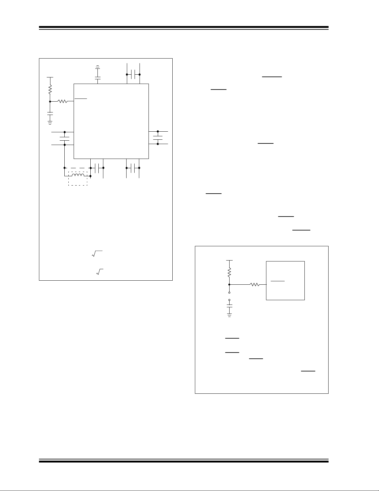
Getting started with the dsPIC33FJ16(GP/MC)101/102
and dsPIC33FJ32(GP/MC)101/102/104 family of 16-bit
Digital Signal Controllers (DSCs) requires attention to a
minimal set of device pin connections before
proceeding with development. The following is a list of
pin names, which must always be connected:
DD and VSS pins
• All V
(see Section 2.2 “Decoupling Capacitors”)
• All AV
•V
•MCLR
• PGECx/PGEDx pins used for In-Circuit Serial
• OSC1 and OSC2 pins when external oscillator
DD and AVSS pins, if present on the device
(regardless if ADC module is not used)
(see Section 2.2 “Decoupling Capacitors”)
CAP
(see Section 2.3 “CPU Logic Filter Capacitor
Connection (V
pin
(see Section 2.4 “Master Clear (MCLR) Pin”)
Programming™ (ICSP™) and debugging purposes
(see Section 2.5 “ICSP Pins”)
source is used
(see Section 2.6 “External Oscillator Pins”)
CAP)”)
2.2 Decoupling Capacitors
The use of decoupling capacitors on every pair of
power supply pins, such as V
AVSS is required.
Consider the following criteria when using decoupling
capacitors:
• Value and type of capacitor: Recommendation
of 0.1 µF (100 nF), 10V-20V. This capacitor
should be a low-ESR and have resonance
frequency in the range of 20 MHz and higher. It is
recommended that ceramic capacitors be used.
• Placement on the printed circuit board: The
decoupling capacitors should be placed as close
to the pins as possible. It is recommended to
place the capacitors on the same side of the
board as the device. If space is constricted, the
capacitor can be placed on another layer on the
PCB using a via; however, ensure that the trace
length from the pin to the capacitor is within
one-quarter inch (6 mm) in length.
• Handling high-frequency noise: If the board is
experiencing high-frequency noise, upward of
tens of MHz, add a second ceramic-type capacitor
in parallel to the above described decoupling
capacitor. The value of the second capacitor can
be in the range of 0.01 µF to 0.001 µF. Place this
second capacitor next to the primary decoupling
capacitor. In high-speed circuit designs, consider
implementing a decade pair of capacitances as
close to the power and ground pins as possible.
For example, 0.1 µF in parallel with 0.001 µF.
• Maximizing performance: On the board layout
from the power supply circuit, run the power and
return traces to the decoupling capacitors first,
and then to the device pins. This ensures that the
decoupling capacitors are first in the power chain.
Equally important is to keep the trace length
between the capacitor and the power pins to a
minimum thereby reducing PCB track inductance.
DD, VSS, AVDD, and
2011-2012 Microchip Technology Inc. DS70652E-page 33
dsPIC33FJ16(GP/MC)101/102 AND dsPIC33FJ32(GP/MC)101/102/104
dsPIC33F
VDD
VSS
VDD
VSS
VSS
VDD
AVDD
AVSS
VDD
VSS
0.1 µF
Ceramic
0.1 µF
Ceramic
0.1 µF
Ceramic
0.1 µF
Ceramic
C
R
V
DD
MCLR
0.1 µF
Ceramic
VCAP
L1
(1)
R1
10 µF
Tantalum
Note 1: As an option, instead of a hard-wired connection, an
inductor (L1) can be substituted between V
DD and
AV
DD to improve ADC noise rejection. The inductor
impedance should be less than 1 and the inductor
capacity greater than 10 mA.
Where:
f
FCNV
2
--------------=
f
1
2 LC
-----------------------=
L
1
2fC
----------------------
2
=
(i.e., ADC conversion rate/2)
Note 1: R 10 k is recommended. A suggested
starting value is 10 k. Ensure that the
MCLR
pin VIH and VIL specifications are met.
2: R1 470 will limit any current flowing into
MCLR
from the external capacitor C, in the
event of MCLR
pin breakdown, due to
Electrostatic Discharge (ESD) or Electrical
Overstress (EOS). Ensure that the MCLR
pin
V
IH and VIL specifications are met.
C
R1
(2)
R
(1)
VDD
MCLR
dsPIC33F
JP
FIGURE 2-1: RECOMMENDED
MINIMUM CONNECTION
The placement of this capacitor should be close to the
VCAP. It is recommended that the trace length not
exceed one-quarter inch (6 mm). Refer to Section 23.2
“On-Chip Voltage Regulator” for details.
2.4 Master Clear (MCLR) Pin
The MCLR pin provides two specific device
functions:
• Device Reset
• Device programming and debugging
During device programming and debugging, the
resistance and capacitance that can be added to the
pin must be considered. Device programmers and
debuggers drive the MCLR
specific voltage levels (VIH and VIL) and fast signal
transitions must not be adversely affected. Therefore,
specific values of R and C will need to be adjusted
based on the application and PCB requirements.
For example, as shown in Figure 2-2, it is
recommended that the capacitor C, be isolated from
the MCLR
pin during programming and debugging
operations.
Place the components shown in Figure 2-2 within
one-quarter inch (6 mm) from the MCLR
pin. Consequently,
pin.
2.2.1 TANK CAPACITORS
On boards with power traces running longer than six
inches in length, it is suggested to use a tank capacitor
for integrated circuits including DSCs to supply a local
power source. The value of the tank capacitor should
be determined based on the trace resistance that connects the power supply source to the device, and the
maximum current drawn by the device in the application. In other words, select the tank capacitor so that it
CAP)
CAP pin must not be
meets the acceptable voltage sag at the device. Typical
values range from 4.7 µF to 47 µF.
2.3 CPU Logic Filter Capacitor
A low-ESR (< 5 Ohms) capacitor is required on the
V
CAP pin, which is used to stabilize the voltage
regulator output voltage. The V
connected to VDD, and must have a capacitor between
4.7 µF and 10 µF, 16V connected to ground. The type
can be ceramic or tantalum. Refer to Section 26.0
“Electrical Characteristics” for additional
information.
DS70652E-page 34 2011-2012 Microchip Technology Inc.
Connection (V
FIGURE 2-2: EXAMPLE OF MCLR PIN
CONNECTIONS
dsPIC33FJ16(GP/MC)101/102 AND dsPIC33FJ32(GP/MC)101/102/104
13
Main Oscillator
Guard Ring
Guard Trace
Secondary
Oscillator
14
15
16
17
18
19
20
2.5 ICSP Pins
The PGECx and PGEDx pins are used for In-Circuit
Serial Programming™ (ICSP™) and debugging purposes. It is recommended to keep the trace length
between the ICSP connector and the ICSP pins on the
device as short as possible. If the ICSP connector is
expected to experience an ESD event, a series resistor
is recommended, with the value in the range of a few
tens of Ohms, not to exceed 100 Ohms.
Pull-up resistors, series diodes, and capacitors on the
PGECx and PGEDx pins are not recommended as they
will interfere with the programmer/debugger communications to the device. If such discrete components are
an application requirement, they should be removed
from the circuit during programming and debugging.
Alternately, refer to the AC/DC characteristics and
timing requirements information in the “dsPIC33F
Flash Programming Specification for Devices with Volatile Configuration Bits” (DS70659) for information on
capacitive loading limits and pin Input Voltage High
IH) and Input Voltage Low (VIL) requirements.
(V
Ensure that the “Communication Channel Select” (i.e.,
PGECx/PGEDx pins) programmed into the device
matches the physical connections for the ICSP to
MPLAB
For more information on ICD 3 and REAL ICE
connection requirements, refer to the following
documents that are available on the Microchip web
site.
• “Using MPLAB
• “MPLAB® ICD 3 Design Advisory” (DS51764)
• “MPLAB
• “Using MPLAB
®
ICD 3 or MPLAB REAL ICE™.
®
ICD 3” (poster) (DS51765)
®
REAL ICE™ In-Circuit Debugger
User’s Guide” (DS51616)
®
REAL ICE™” (poster) (DS51749)
2.6 External Oscillator Pins
Many DSCs have options for at least two oscillators: a
high-frequency primary oscillator and a low-frequency
secondary oscillator (refer to Section 8.0 “Oscillator
Configuration” for details).
The oscillator circuit should be placed on the same
side of the board as the device. Also, place the
oscillator circuit close to the respective oscillator pins,
not exceeding one-half inch (12 mm) distance
between them. The load capacitors should be placed
next to the oscillator itself, on the same side of the
board. Use a grounded copper pour around the
oscillator circuit to isolate them from surrounding
circuits. The grounded copper pour should be routed
directly to the MCU ground. Do not run any signal
traces or power traces inside the ground pour. Also, if
using a two-sided board, avoid any traces on the
other side of the board where the crystal is placed. A
suggested layout is shown in Figure 2-3.
FIGURE 2-3: SUGGESTED PLACEMENT
OF THE OSCILLATOR
CIRCUIT
2011-2012 Microchip Technology Inc. DS70652E-page 35

dsPIC33FJ16(GP/MC)101/102 AND dsPIC33FJ32(GP/MC)101/102/104
2.7 Oscillator Value Conditions on Device Start-up
If the PLL of the target device is enabled and
configured for the device start-up oscillator, the
maximum oscillator source frequency must be limited
to 4 MHz < F
IN < 8 MHz (for ECPLL mode) to comply with device
F
PLL start-up conditions. HSPLL mode is not supported.
This means that if the external oscillator frequency is
outside this range, the application must start-up in the
FRC mode first. The fixed PLL settings of 4x after a
POR with an oscillator frequency outside this range will
violate the device operating speed.
Once the device powers up, the application firmware
can enable the PLL, and then perform a clock switch to
the Oscillator + PLL clock source. Note that clock
switching must be enabled in the device Configuration
Word.
IN < 8 MHz (for MSPLL mode) or 3 MHz <
2.8 Configuration of Analog and Digital Pins During ICSP Operations
If MPLAB ICD 3 or MPLAB REAL ICE in-circuit
emulator is selected as a debugger, it automatically
initializes all of the Analog-to-Digital input pins (ANx) as
“digital” pins, by setting all bits in the AD1PCFGL
register.
The bits in the register that correspond to the
Analog-to-Digital pins that are initialized by MPLAB
ICD 3 or MPLAB REAL ICE in-circuit emulator, must
not be cleared by the user application firmware;
otherwise, communication errors will result between
the debugger and the device.
If your application needs to use certain
Analog-to-Digital pins as analog input pins during the
debug session, the user application must clear the
corresponding bits in the AD1PCFGL register during
initialization of the ADC module.
When MPLAB ICD 3 or MPLAB REAL ICE in-circuit
emulator is used as a programmer, the user application
firmware must correctly configure the AD1PCFGL
register. Automatic initialization of this register is only
done during debugger operation. Failure to correctly
configure the register(s) will result in all
Analog-to-Digital pins being recognized as analog input
pins, resulting in the port value being read as a logic ‘0’,
which may affect user application functionality.
2.9 Unused I/Os
Unused I/O pins should be configured as outputs and
driven to a logic-low state.
Alternately, connect a 1k to 10k resistor between V
and unused pins.
SS
DS70652E-page 36 2011-2012 Microchip Technology Inc.

dsPIC33FJ16(GP/MC)101/102 AND dsPIC33FJ32(GP/MC)101/102/104
3.0 CPU
Note 1: This data sheet summarizes the features
of the dsPIC33FJ16(GP/MC)101/102
and dsPIC33FJ32(GP/MC)101/102/104
family devices. It is not intended to be a
comprehensive reference source. To
complement the information in this data
sheet, refer to Section 2. “CPU”
(DS70204) in the “dsPIC33F/PIC24H
Family Reference Manual”, which is
available from the Microchip web site
(www.microchip.com).
2: Some registers and associated bits
described in this section may not be
available on all devices. Refer to
Section 4.0 “Memory Organization” in
this data sheet for device-specific register
and bit information.
The dsPIC33FJ16(GP/MC)101/102 and
dsPIC33FJ32(GP/MC)101/102/104 CPU module has
a 16-bit (data) modified Harvard architecture with an
enhanced instruction set, including significant support
for DSP. The CPU has a 24-bit instruction word with a
variable length opcode field. The Program Counter
(PC) is 23 bits wide and addresses up to 4M x 24 bits
of user program memory space. The actual amount of
program memory implemented varies by device. A
single-cycle instruction prefetch mechanism is used to
help maintain throughput and provides predictable
execution. All instructions execute in a single cycle,
with the exception of instructions that change the
program flow, the double-word move (MOV.D)
instruction and the table instructions. Overhead-free
program loop constructs are supported using the DO
and REPEAT instructions, both of which are
interruptible at any point.
The dsPIC33FJ16(GP/MC)101/102 and
dsPIC33FJ32(GP/MC)101/102/104 devices have sixteen, 16-bit working registers in the programmer’s
model. Each of the working registers can serve as a
data, address, or address offset register. The 16th
working register (W15) operates as a software Stack
Pointer (SP) for interrupts and calls.
There are two classes of instruction in the
dsPIC33FJ16(GP/MC)101/102 and dsPIC33FJ32(GP/
MC)101/102/104 devices: MCU and DSP. These two
instruction classes are seamlessly integrated into a single CPU. The instruction set includes many addressing
modes and is designed for optimum C compiler efficiency. For most instructions, dsPIC33FJ16(GP/
MC)101/102 and dsPIC33FJ32(GP/MC)101/102/104
devices are capable of executing a data (or program
data) memory read, a working register (data) read, a
data memory write, and a program (instruction) memory
read per instruction cycle. As a result, three parameter
instructions can be supported, allowing A + B = C
operations to be executed in a single cycle.
A block diagram of the CPU is shown in Figure 3-1, and
the programmer’s model for the dsPIC33FJ16(GP/
MC)101/102 and dsPIC33FJ32(GP/MC)101/102/104
is shown in Figure 3-2.
3.1 Data Addressing Overview
The data space can be addressed as 32K words or
64 Kbytes and is split into two blocks, referred to as X
and Y data memory. Each memory block has its own
independent Address Generation Unit (AGU). The
MCU class of instructions operates solely through the
X memory AGU, which accesses the entire memory
map as one linear data space. Certain DSP instructions
operate through the X and Y AGUs to support dual
operand reads, which splits the data address space
into two parts. The X and Y data space boundary is
device-specific.
Overhead-free circular buffers (Modulo Addressing
mode) are supported in both X and Y address spaces.
The Modulo Addressing removes the software
boundary checking overhead for DSP algorithms.
Furthermore, the X AGU circular addressing can be
used with any of the MCU class of instructions. The X
AGU also supports Bit-Reversed Addressing to greatly
simplify input or output data reordering for radix-2 FFT
algorithms.
The upper 32 Kbytes of the data space memory map
can optionally be mapped into program space at any
16K program word boundary defined by the 8-bit
Program Space Visibility Page (PSVPAG) register. The
program-to-data-space mapping feature lets any
instruction access program space as if it were data
space.
3.2 DSP Engine Overview
The DSP engine features a high-speed 17-bit by 17-bit
multiplier, a 40-bit ALU, two 40-bit saturating
accumulators, and a 40-bit bidirectional barrel shifter.
The barrel shifter is capable of shifting a 40-bit value up
to 16 bits right or left, in a single cycle. The DSP instructions operate seamlessly with all other instructions and
have been designed for optimal real-time performance.
The MAC instruction and other associated instructions
can concurrently fetch two data operands from memory, while multiplying two W registers and accumulating
and optionally saturating the result in the same cycle.
This instruction functionality requires that the RAM data
space be split for these instructions and linear for all
others. Data space partitioning is achieved in a transparent and flexible manner through dedicating certain
working registers to each address space.
2011-2012 Microchip Technology Inc. DS70652E-page 37
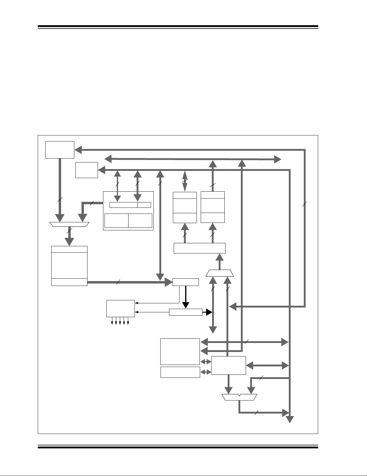
dsPIC33FJ16(GP/MC)101/102 AND dsPIC33FJ32(GP/MC)101/102/104
Instruction
Decode and
Control
PCH PCL
Program Counter
16-Bit ALU
24
23
Instruction Reg
PCU
16 x 16
W Register Array
ROM Latch
EA MUX
Interrupt
Controller
Stac k
Control
Logic
Loop
Control
Logic
Data Latch
Address
Latch
Control Signals
to Various Blocks
Literal Data
16
16
16
To Peripheral Modules
Data Latch
Address
Latch
16
X RAM
Y RAM
Address Generator Units
16
Y Data Bus
X Data Bus
DSP Engine
Divide Support
16
16
23
23
16
8
PSV and Table
Data Access
Control Block
16
16
16
16
Program Memory
Data Latch
Address Latch
3.3 Special MCU Features
The dsPIC33FJ16(GP/MC)101/102 and
dsPIC33FJ32(GP/MC)101/102/104 supports 16/16
The dsPIC33FJ16(GP/MC)101/102 and
dsPIC33FJ32(GP/MC)101/102/104 features a 17-bit
by 17-bit single-cycle multiplier that is shared by both
the MCU ALU and DSP engine. The multiplier can perform signed, unsigned and mixed-sign multiplication.
Using a 17-bit by 17-bit multiplier for 16-bit by 16-bit
multiplication not only allows you to perform mixed-sign
multiplication, it also achieves accurate results for
special operations, such as (-1.0) x (-1.0).
and 32/16 divide operations, both fractional and
integer. All divide instructions are iterative operations.
They must be executed within a REPEAT loop, resulting
in a total execution time of 19 instruction cycles. The
divide operation can be interrupted during any of those
19 cycles without loss of data.
A 40-bit barrel shifter is used to perform up to a 16-bit
left or right shift in a single cycle. The barrel shifter can
be used by both MCU and DSP instructions.
FIGURE 3-1: dsPIC33FJ16(GP/MC)101/102 AND dsPIC33FJ32(GP/MC)101/102/104
CPU CORE BLOCK DIAGRAM
DS70652E-page 38 2011-2012 Microchip Technology Inc.

dsPIC33FJ16(GP/MC)101/102 AND dsPIC33FJ32(GP/MC)101/102/104
PC22
PC0
7
0
D0D15
Program Counter
Data Table Page Address
STATUS Register
Working Registers
DSP Operand
Registers
W1
W2
W3
W4
W5
W6
W7
W8
W9
W10
W11
W12/DSP Offset
W13/DSP Write Back
W14/Frame Pointer
W15/Stack Pointer
DSP Address
Registers
AD39 AD0AD31
DSP
Accumulators
ACCA
ACCB
7
0
Program Space Visibility Page Address
Z
0
OA OB SA SB
RCOUNT
15
0
REPEAT Loop Counter
DCOUNT
15
0
DO Loop Counter
DOSTART
22
0
DO Loop Start Address
IPL2 IPL1
SPLIM
Stack Pointer Limit Register
AD15
SRL
PUSH.S Shadow
DO Shadow
OAB SAB
15
0
Core Configuration Register
Legend
CORCON
DA DC
RA
N
TBLPAG
PSVPAG
IPL0 OV
W0/WREG
SRH
DO Loop End Address
DOEND
22
C
FIGURE 3-2: dsPIC33FJ16(GP/MC)101/102 AND dsPIC33FJ32(GP/MC)101/102/104
PROGRAMMER’S MODEL
2011-2012 Microchip Technology Inc. DS70652E-page 39
dsPIC33FJ16(GP/MC)101/102 AND dsPIC33FJ32(GP/MC)101/102/104
3.4 CPU Control Registers
REGISTER 3-1: SR: CPU STATUS REGISTER
R-0 R-0 R/C-0 R/C-0 R-0 R/C-0 R-0 R/W-0
OA OB SA
(1)
bit 15 bit 8
SB
(1)
OAB SAB DA DC
R/W-0
(3)
IPL<2:0>
R/W-0
(3)
(2)
R/W-0
(3)
R-0 R/W-0 R/W-0 R/W-0 R/W-0
RA N OV Z C
bit 7 bit 0
Legend: C = Clearable bit
R = Readable bit W = Writable bit U = Unimplemented bit, read as ‘0’
-n = Value at POR ‘1’ = Bit is set ‘0’ = Bit is cleared x = Bit is unknown
bit 15 OA: Accumulator A Overflow Status bit
1 = Accumulator A overflowed
0 = Accumulator A has not overflowed
bit 14 OB: Accumulator B Overflow Status bit
1 = Accumulator B overflowed
0 = Accumulator B has not overflowed
bit 13 SA: Accumulator A Saturation ‘Sticky’ Status bit
(1)
1 = Accumulator A is saturated or has been saturated at some time
0 = Accumulator A is not saturated
bit 12 SB: Accumulator B Saturation ‘Sticky’ Status bit
(1)
1 = Accumulator B is saturated or has been saturated at some time
0 = Accumulator B is not saturated
bit 11 OAB: OA || OB Combined Accumulator Overflow Status bit
1 = Accumulators A or B have overflowed
0 = Neither Accumulators A or B have overflowed
bit 10 SAB: SA || SB Combined Accumulator ‘Sticky’ Status bit
1 = Accumulators A or B are saturated or have been saturated at some time in the past
0 = Neither Accumulator A or B are saturated
This bit may be read or cleared (not set). Clearing this bit will clear SA and SB.
bit 9 DA: DO Loop Active bit
1 = DO loop in progress
0 = DO loop not in progress
bit 8 DC: MCU ALU Half Carry/Borrow
bit
1 = A carry-out from the 4th low-order bit (for byte-sized data) or 8th low-order bit (for word-sized data)
of the result occurred
0 = No carry-out from the 4th low-order bit (for byte-sized data) or 8th low-order bit (for word-sized
data) of the result occurred
Note 1: This bit can be read or cleared (not set).
2: The IPL<2:0> bits are concatenated with the IPL<3> bit (CORCON<3>) to form the CPU Interrupt Priority
Level. The value in parentheses indicates the IPL if IPL<3> = 1. User interrupts are disabled when
IPL<3> = 1.
3: The IPL<2:0> Status bits are read-only when NSTDIS = 1 (INTCON1<15>).
DS70652E-page 40 2011-2012 Microchip Technology Inc.

dsPIC33FJ16(GP/MC)101/102 AND dsPIC33FJ32(GP/MC)101/102/104
REGISTER 3-1: SR: CPU STATUS REGISTER (CONTINUED)
bit 7-5 IPL<2:0>: CPU Interrupt Priority Level Status bits
111 = CPU Interrupt Priority Level is 7 (15), user interrupts are disabled
110 = CPU Interrupt Priority Level is 6 (14)
101 = CPU Interrupt Priority Level is 5 (13)
100 = CPU Interrupt Priority Level is 4 (12)
011 = CPU Interrupt Priority Level is 3 (11)
010 = CPU Interrupt Priority Level is 2 (10)
001 = CPU Interrupt Priority Level is 1 (9)
000 = CPU Interrupt Priority Level is 0 (8)
bit 4 RA: REPEAT Loop Active bit
1 = REPEAT loop in progress
0 = REPEAT loop not in progress
bit 3 N: MCU ALU Negative bit
1 = Result was negative
0 = Result was non-negative (zero or positive)
bit 2 OV: MCU ALU Overflow bit
This bit is used for signed arithmetic (2’s complement). It indicates an overflow of a magnitude that
causes the sign bit to change state.
1 = Overflow occurred for signed arithmetic (in this arithmetic operation)
0 = No overflow occurred
bit 1 Z: MCU ALU Zero bit
1 = An operation that affects the Z bit has set it at some time in the past
0 = The most recent operation that affects the Z bit has cleared it (i.e., a non-zero result)
bit 0 C: MCU ALU Carry/Borrow
1 = A carry-out from the Most Significant bit of the result occurred
0 = No carry-out from the Most Significant bit of the result occurred
bit
(2,3)
Note 1: This bit can be read or cleared (not set).
2: The IPL<2:0> bits are concatenated with the IPL<3> bit (CORCON<3>) to form the CPU Interrupt Priority
Level. The value in parentheses indicates the IPL if IPL<3> = 1. User interrupts are disabled when
IPL<3> = 1.
3: The IPL<2:0> Status bits are read-only when NSTDIS = 1 (INTCON1<15>).
2011-2012 Microchip Technology Inc. DS70652E-page 41

dsPIC33FJ16(GP/MC)101/102 AND dsPIC33FJ32(GP/MC)101/102/104
REGISTER 3-2: CORCON: CORE CONTROL REGISTER
U-0 U-0 U-0 R/W-0 R/W-0 R-0 R-0 R-0
— — —USEDT
(1)
DL<2:0>
bit 15 bit 8
R/W-0 R/W-0 R/W-1 R/W-0 R/C-0 R/W-0 R/W-0 R/W-0
SATA SATB SATDW ACCSAT IPL3
(2)
PSV RND IF
bit 7 bit 0
Legend: C = Clearable bit
R = Readable bit W = Writable bit -n = Value at POR ‘1’ = Bit is set
0’ = Bit is cleared ‘x = Bit is unknown U = Unimplemented bit, read as ‘0’
bit 15-13 Unimplemented: Read as ‘0’
bit 12 US: DSP Multiply Unsigned/Signed Control bit
1 = DSP engine multiplies are unsigned
0 = DSP engine multiplies are signed
bit 11 EDT: Early DO Loop Termination Control bit
(1)
1 = Terminates executing DO loop at end of current loop iteration
0 = No effect
bit 10-8 DL<2:0>: DO Loop Nesting Level Status bits
111 = 7 DO loops are active
•
•
•
001 = 1 DO loop is active
000 = 0 DO loops is active
bit 7 SATA: ACCA Saturation Enable bit
1 = Accumulator A saturation is enabled
0 = Accumulator A saturation is disabled
bit 6 SATB: ACCB Saturation Enable bit
1 = Accumulator B saturation is enabled
0 = Accumulator B saturation is disabled
bit 5 SATDW: Data Space Write from DSP Engine Saturation Enable bit
1 = Data space write saturation is enabled
0 = Data space write saturation is disabled
bit 4 ACCSAT: Accumulator Saturation Mode Select bit
1 = 9.31 saturation (super saturation)
0 = 1.31 saturation (normal saturation)
bit 3 IPL3: CPU Interrupt Priority Level Status bit 3
(2)
1 = CPU Interrupt Priority Level is greater than 7
0 = CPU Interrupt Priority Level is 7 or less
bit 2 PSV: Program Space Visibility in Data Space Enable bit
1 = Program space is visible in data space
0 = Program space is not visible in data space
bit 1 RND: Rounding Mode Select bit
1 = Biased (conventional) rounding is enabled
0 = Unbiased (convergent) rounding is enabled
bit 0 IF: Integer or Fractional Multiplier Mode Select bit
1 = Integer mode is enabled for DSP multiply ops
0 = Fractional mode is enabled for DSP multiply ops
Note 1: This bit will always read as ‘0’.
2: The IPL3 bit is concatenated with the IPL<2:0> bits (SR<7:5>) to form the CPU Interrupt Priority Level.
DS70652E-page 42 2011-2012 Microchip Technology Inc.

dsPIC33FJ16(GP/MC)101/102 AND dsPIC33FJ32(GP/MC)101/102/104
3.5 Arithmetic Logic Unit (ALU)
The dsPIC33FJ16(GP/MC)101/102 and
dsPIC33FJ32(GP/MC)101/102/104 ALU is 16 bits
wide and is capable of addition, subtraction, bit shifts,
and logic operations. Unless otherwise mentioned,
arithmetic operations are 2’s complement in nature.
Depending on the operation, the ALU can affect the
values of the Carry (C), Zero (Z), Negative (N), Overflow (OV), and Digit Carry (DC) Status bits in the SR
register. The C and DC Status bits operate as Borrow
and Digit Borrow bits, respectively, for subtraction
operations.
The ALU can perform 8-bit or 16-bit operations,
depending on the mode of the instruction that is used.
Data for the ALU operation can come from the W
register array or data memory, depending on the
addressing mode of the instruction. Likewise, output
data from the ALU can be written to the W register array
or a data memory location.
Refer to the “16-Bit MCU and DSC Programmer’s
Reference Manual” (DS70157) for information on the
SR bits affected by each instruction.
The dsPIC33FJ16(GP/MC)101/102 and
dsPIC33FJ32(GP/MC)101/102/104 CPU incorporates hardware support for both multiplication and
division. This includes a dedicated hardware multiplier
and support hardware for 16-bit-divisor division.
3.5.1 MULTIPLIER
Using the high-speed 17-bit x 17-bit multiplier of the
DSP engine, the ALU supports unsigned, signed or
mixed-sign operation in several MCU multiplication
modes:
• 16-bit x 16-bit signed
• 16-bit x 16-bit unsigned
• 16-bit signed x 5-bit (literal) unsigned
• 16-bit unsigned x 16-bit unsigned
• 16-bit unsigned x 5-bit (literal) unsigned
• 16-bit unsigned x 16-bit signed
• 8-bit unsigned x 8-bit unsigned
3.5.2 DIVIDER
The divide block supports 32-bit/16-bit and 16-bit/16-bit
signed and unsigned integer divide operations with the
following data sizes:
• 32-bit signed/16-bit signed divide
• 32-bit unsigned/16-bit unsigned divide
• 16-bit signed/16-bit signed divide
• 16-bit unsigned/16-bit unsigned divide
The quotient for all divide instructions ends up in W0
and the remainder in W1. The 16-bit signed and
unsigned DIV instructions can specify any W register
for both the 16-bit divisor (Wn) and any W register
(aligned) pair (W(m + 1):Wm) for the 32-bit dividend.
The divide algorithm takes one cycle per bit of divisor,
so both 32-bit/16-bit and 16-bit/16-bit instructions take
the same number of cycles to execute.
3.6 DSP Engine
The DSP engine consists of a high-speed 17-bit x
17-bit multiplier, a barrel shifter and a 40-bit adder/
subtracter (with two target accumulators, round and
saturation logic).
The dsPIC33FJ16(GP/MC)101/102 and
dsPIC33FJ32(GP/MC)101/102/104 is a single-cycle
instruction flow architecture; therefore, concurrent
operation of the DSP engine with MCU instruction flow
is not possible. However, some MCU ALU and DSP
engine resources can be used concurrently by the
same instruction (e.g., ED, EDAC).
The DSP engine can also perform inherent accumulator-to-accumulator operations that require no additional
data. These instructions are ADD, SUB, and NEG.
The DSP engine has options selected through bits in
the CPU Core Control register (CORCON), as listed
below:
• Fractional or Integer DSP Multiply (IF)
• Signed or Unsigned DSP Multiply (US)
• Conventional or Convergent Rounding (RND)
• Automatic Saturation On/Off for ACCA (SATA)
• Automatic Saturation On/Off for ACCB (SATB)
• Automatic Saturation On/Off for Writes to Data
Memory (SATDW)
• Accumulator Saturation mode Selection (ACCSAT)
A block diagram of the DSP engine is shown in
Figure 3-3.
TABLE 3-1: DSP INSTRUCTIONS
SUMMARY
Instruction
CLR A = 0 Ye s
ED A = (x – y)
EDAC A = A + (x – y)
MAC A = A + (x * y) Yes
MAC A = A + x
MOVSAC No change in A Yes
MPY A = x * y No
MPY A = x
MPY.N A = – x * y No
MSC A = A – x * y Yes
Algebraic
Operation
2
2
2
2
ACC Write
Back
No
No
No
No
2011-2012 Microchip Technology Inc. DS70652E-page 43
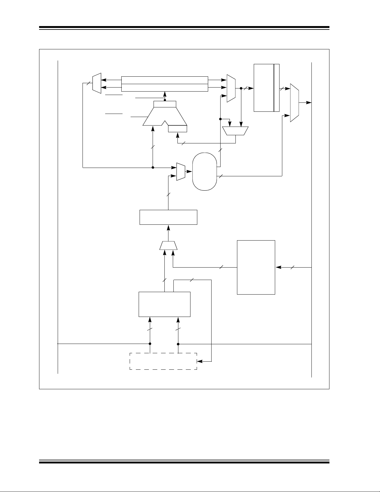
dsPIC33FJ16(GP/MC)101/102 AND dsPIC33FJ32(GP/MC)101/102/104
Zero Backfill
Sign-Extend
Barrel
Shifter
40-Bit Accumulator A
40-Bit Accumulator B
Round
Logic
X Data Bus
To/From W Array
Adder
Saturate
Negate
32
32
33
16
16
16
16
40
40
40
40
S
a
t
u
r
a
t
e
Y Data Bus
40
Carry/Borrow Out
Carry/Borrow In
16
40
Multiplier/Scaler
17-Bit
FIGURE 3-3: DSP ENGINE BLOCK DIAGRAM
DS70652E-page 44 2011-2012 Microchip Technology Inc.

dsPIC33FJ16(GP/MC)101/102 AND dsPIC33FJ32(GP/MC)101/102/104
3.6.1 MULTIPLIER
The 17-bit x 17-bit multiplier is capable of signed or
unsigned operation and can multiplex its output using a
scaler to support either 1.31 fractional (Q31) or 32-bit
integer results. Unsigned operands are zero-extended
into the 17th bit of the multiplier input value. Signed
operands are sign-extended into the 17th bit of the
multiplier input value. The output of the 17-bit x 17-bit
multiplier/scaler is a 33-bit value that is sign-extended
to 40 bits. Integer data is inherently represented as a
signed 2’s complement value, where the Most Significant bit (MSb) is defined as a sign bit. The range of an
N-bit 2’s complement integer is -2
N-1
to 2
N-1
– 1.
• For a 16-bit integer, the data range is -32768
(0x8000) to 32767 (0x7FFF) including 0.
• For a 32-bit integer, the data range is
-2,147,483,648 (0x8000 0000) to 2,147,483,647
(0x7FFF FFFF).
When the multiplier is configured for fractional
multiplication, the data is represented as a 2’s
complement fraction, where the MSb is defined as a
sign bit and the radix point is implied to lie just after the
sign bit (QX format). The range of an N-bit 2’s
complement fraction with this implied radix point is -1.0
to (1 – 2
is -1.0 (0x8000) to 0.999969482 (0x7FFF) including 0
and has a precision of 3.01518x10
mode, the 16 x 16 multiply operation generates a
1.31 product that has a precision of 4.65661 x 10
1-N
). For a 16-bit fraction, the Q15 data range
-5
. In Fractional
-10
.
The same multiplier is used to support the MCU
multiply instructions, which include integer 16-bit
signed, unsigned and mixed sign multiply operations.
The MUL instruction can be directed to use byte or
word-sized operands. Byte operands will direct a 16-bit
result, and word operands will direct a 32-bit result to
the specified register(s) in the W array.
3.6.2 DATA ACCUMULATORS AND
ADDER/SUBTRACTER
The data accumulator consists of a 40-bit adder/
subtracter with automatic sign extension logic. It can
select one of two accumulators (A or B) as its preaccumulation source and post-accumulation
destination. For the ADD and LAC instructions, the data
to be accumulated or loaded can be optionally scaled
using the barrel shifter prior to accumulation.
3.6.2.1 Adder/Subtracter, Overflow and
Saturation
The adder/subtracter is a 40-bit adder with an optional
zero input into one side, and either true or complement
data into the other input.
• In the case of addition, the Carry/B
active-high and the other input is true data (not
complemented).
• In the case of subtraction, the Carry/Borrow
is active-low and the other input is complemented.
The adder/subtracter generates Overflow Status bits,
SA/SB and OA/OB, which are latched and reflected in
the STATUS register:
• Overflow from bit 39: this is a catastrophic
overflow in which the sign of the accumulator is
destroyed.
• Overflow into guard bits 32 through 39: this is a
recoverable overflow. This bit is set whenever all
the guard bits are not identical to each other.
The adder has an additional saturation block that
controls accumulator data saturation, if selected. It
uses the result of the adder, the Overflow Status bits
described previously, and the SAT<A:B>
(CORCON<7:6>) and ACCSAT (CORCON<4>) mode
control bits to determine when and to what value, to
saturate.
Six STATUS register bits support saturation and
overflow:
• OA: ACCA overflowed into guard bits
• OB: ACCB overflowed into guard bits
• SA: ACCA saturated (bit 31 overflow and
saturation)
or
ACCA overflowed into guard bits and
saturated (bit 39 overflow and saturation)
• SB: ACCB saturated (bit 31 overflow and
saturation)
or
ACCB overflowed into guard bits and
saturated (bit 39 overflow and saturation)
• OAB: Logical OR of OA and OB
• SAB: Logical OR of SA and SB
The OA and OB bits are modified each time data
passes through the adder/subtracter. When set, they
indicate that the most recent operation has overflowed
into the accumulator guard bits (bits 32 through 39).
The OA and OB bits can also optionally generate an
arithmetic warning trap when OA and OB are set and
the corresponding Overflow Trap Flag Enable bits
(OVATE, OVBTE) in the INTCON1 register are set
(refer to Section 7.0 “Interrupt Controller”). This
allows the user application to take immediate action; for
example, to correct system gain.
orrow input is
input
2011-2012 Microchip Technology Inc. DS70652E-page 45

dsPIC33FJ16(GP/MC)101/102 AND dsPIC33FJ32(GP/MC)101/102/104
The SA and SB bits are modified each time data
passes through the adder/subtracter, but can only be
cleared by the user application. When set, they indicate
that the accumulator has overflowed its maximum
range (bit 31 for 32-bit saturation or bit 39 for 40-bit
saturation) and will be saturated (if saturation is
enabled). When saturation is not enabled, SA and SB
default to bit 39 overflow, and therefore, indicate that a
catastrophic overflow has occurred. If the COVTE bit in
the INTCON1 register is set, the SA and SB bits will
generate an arithmetic warning trap when saturation is
disabled.
The Overflow and Saturation Status bits can optionally
be viewed in the STATUS Register (SR) as the logical
OR of OA and OB (in bit OAB) and the logical OR of SA
and SB (in bit SAB). Programmers can check one bit in
the STATUS register to determine whether either
accumulator has overflowed, or one bit to determine
whether either accumulator has saturated. This is
useful for complex number arithmetic, which typically
uses both accumulators.
The device supports three Saturation and Overflow
modes:
• Bit 39 Overflow and Saturation:
When bit 39 overflow and saturation occurs, the
saturation logic loads the maximally positive 9.31
value (0x7FFFFFFFFF) or maximally negative 9.31
value (0x8000000000) into the target accumulator.
The SA or SB bit is set and remains set until
cleared by the user application. This condition is
referred to as ‘super saturation’ and provides protection against erroneous data or unexpected
algorithm problems (such as gain calculations).
• Bit 31 Overflow and Saturation:
When bit 31 overflow and saturation occurs, the
saturation logic then loads the maximally positive
1.31 value (0x007FFFFFFF) or maximally negative 1.31 value (0x0080000000) into the target
accumulator. The SA or SB bit is set and remains
set until cleared by the user application. When
this Saturation mode is in effect, the guard bits are
not used, so the OA, OB or OAB bits are never
set.
• Bit 39 Catastrophic Overflow:
The bit 39 Overflow Status bit from the adder is
used to set the SA or SB bit, which remains set
until cleared by the user application. No saturation
operation is performed, and the accumulator is
allowed to overflow, destroying its sign. If the
COVTE bit in the INTCON1 register is set, a
catastrophic overflow can initiate a trap exception.
3.6.3 ACCUMULATOR ‘WRITE BACK’
The MAC class of instructions (with the exception of
MPY, MPY.N, ED, and EDAC) can optionally write a
rounded version of the high word (bits 31 through 16)
of the accumulator which is not targeted by the instruction into data space memory. The write is performed
across the X bus into combined X and Y address
space. The following addressing modes are supported:
• W13, Register Direct:
The rounded contents of the non-target
accumulator are written into W13 as a
1.15 fraction.
• [W13] + = 2, Register Indirect with Post-Increment:
The rounded contents of the non-target accumulator are written into the address pointed to by
W13 as a 1.15 fraction. W13 is then incremented
by 2 (for a word write).
3.6.3.1 Round Logic
The round logic is a combinational block that performs
a conventional (biased) or convergent (unbiased)
round function during an accumulator write (store). The
Round mode is determined by the state of the RND bit
in the CORCON register. It generates a 16-bit,
1.15 data value that is passed to the data space write
saturation logic. If rounding is not indicated by the
instruction, a truncated 1.15 data value is stored and
the least significant word (lsw) is simply discarded.
Conventional rounding will zero-extend bit 15 of the
accumulator and will add it to the ACCxH word (bits 16
through 31 of the accumulator).
• If the ACCxL word (bits 0 through 15 of the accumulator) is between 0x8000 and 0xFFFF (0x8000
included), ACCxH is incremented.
• If ACCxL is between 0x0000 and 0x7FFF, ACCxH
is left unchanged.
A consequence of this algorithm is that over a succession of random rounding operations, the value tends to
be biased slightly positive.
Convergent (or unbiased) rounding operates in the
same manner as conventional rounding, except when
ACCxL equals 0x8000. In this case, the Least
Significant bit (LSb), bit 16 of the accumulator, of
ACCxH is examined:
• If it is ‘1’, ACCxH is incremented.
• If it is ‘0’, ACCxH is not modified.
Assuming that bit 16 is effectively random in nature,
this scheme removes any rounding bias that may
accumulate.
DS70652E-page 46 2011-2012 Microchip Technology Inc.

dsPIC33FJ16(GP/MC)101/102 AND dsPIC33FJ32(GP/MC)101/102/104
The SAC and SAC.R instructions store either a
truncated (SAC), or rounded (SAC.R) version of the
contents of the target accumulator to data memory via
the X bus, subject to data saturation (see
Section 3.6.3.2 “Data Space Write Saturation”). For
the MAC class of instructions, the accumulator writeback operation functions in the same manner,
addressing combined MCU (X and Y) data space
though the X bus. For this class of instructions, the data
is always subject to rounding.
3.6.3.2 Data Space Write Saturation
In addition to adder/subtracter saturation, writes to data
space can also be saturated, but without affecting the
contents of the source accumulator. The data space
write saturation logic block accepts a 16-bit,
1.15 fractional value from the round logic block as its
input, together with overflow status from the original
source (accumulator) and the 16-bit round adder.
These inputs are combined and used to select the
appropriate 1.15 fractional value as output to write to
data space memory.
If the SATDW bit in the CORCON register is set, data
(after rounding or truncation) is tested for overflow and
adjusted accordingly:
• For input data greater than 0x007FFF, data
written to memory is forced to the maximum
positive 1.15 value, 0x7FFF.
• For input data less than 0xFF8000, data written to
memory is forced to the maximum negative
1.15 value, 0x8000.
The MSb of the source (bit 39) is used to determine the
sign of the operand being tested.
If the SATDW bit in the CORCON register is not set, the
input data is always passed through unmodified under
all conditions.
3.6.4 BARREL SHIFTER
The barrel shifter can perform up to 16-bit arithmetic or
logic right shifts, or up to 16-bit left shifts, in a single
cycle. The source can be either of the two DSP
accumulators or the X bus (to support multi-bit shifts of
register or memory data).
The shifter requires a signed binary value to determine
both the magnitude (number of bits) and direction of the
shift operation. A positive value shifts the operand right.
A negative value shifts the operand left. A value of ‘0’
does not modify the operand.
The barrel shifter is 40 bits wide, thereby obtaining a
40-bit result for DSP shift operations and a 16-bit result
for MCU shift operations. Data from the X bus is
presented to the barrel shifter between Bit Positions 16
and 31 for right shifts, and between Bit Positions 0 and
16 for left shifts.
2011-2012 Microchip Technology Inc. DS70652E-page 47

dsPIC33FJ16(GP/MC)101/102 AND dsPIC33FJ32(GP/MC)101/102/104
NOTES:
DS70652E-page 48 2011-2012 Microchip Technology Inc.
dsPIC33FJ16(GP/MC)101/102 AND dsPIC33FJ32(GP/MC)101/102/104
Reset Address
0x000000
0x0000FE
0x000002
0x000100
Device Configuration
User Program
Flash Memory
0x002BFC
0x002BFA
(5.6K instructions)
0x800000
0xF80000
Shadow Registers
0xF80017
DEVID (2)
0xFEFFFE
0xFF0000
0xFFFFFE
0xF7FFFE
Unimplemented
(Read ‘
0
’s)
GOTO
Instruction
0x000004
Reserved
0x7FFFFE
Reserved
0x000200
0x0001FE
0x000104
Alternate Vector Table
Reserved
Interrupt Vector Table
Configuration Memory Space
User Memory Space
Flash Configuration
Words
(1)
0x002COO
0x002BFE
Note 1: On Reset, these bits are automatically copied into the device Configuration Shadow registers.
0xF80018
4.0 MEMORY ORGANIZATION
Note: This data sheet summarizes the features
of the dsPIC33FJ16(GP/MC)101/102 and
dsPIC33FJ32(GP/MC)101/102/104 family
devices. However, it is not intended to be
a comprehensive reference source. To
complement the information in this data
sheet, refer to Section 3. “Data Memory”
(DS70202) and Section 4. “Program
Memory” (DS70203) in the “dsPIC33F/
PIC24H Family Reference Manual”, which
are available from the Microchip web site
(www.microchip.com).
4.1 Program Address Space
The program address memory space of the
dsPIC33FJ16(GP/MC)101/102 and dsPIC33FJ32(GP/
MC)101/102/104 devices is 4M instructions. The space
is addressable by a 24-bit value derived either from the
23-bit Program Counter (PC) during program execution,
or from table operation or data space remapping as
described in Section 4.6 “Interfacing Program and
Data Memory Spaces”.
User application access to the program memory space
is restricted to the lower half of the address range
(0x000000 to 0x7FFFFF). The exception is the use of
TBLRD/TBLWT operations, which use TBLPAG<7> to
permit access to the Configuration bits and Device ID
The device architecture features separate program and
data memory spaces and buses. This architecture also
allows the direct access of program memory from the
data space during code execution.
sections of the configuration memory space.
The memory maps for the dsPIC33FJ16(GP/MC)101/
102 and dsPIC33FJ32(GP/MC)101/102/104 family of
devices re shown in Figure 4-1 and Figure 4-2.
FIGURE 4-1: PROGRAM MEMORY MAP FOR dsPIC33FJ16(GP/MC)101/102 DEVICES
2011-2012 Microchip Technology Inc. DS70652E-page 49

dsPIC33FJ16(GP/MC)101/102 AND dsPIC33FJ32(GP/MC)101/102/104
0x000000
0x0000FE
0x000002
0x000100
Device Configuration
User Program
Flash Memory
0x0057FC
0x0057FA
(11.2K instructions)
0x800000
0xF80000
Shadow Registers
0xF80020
DEVID (2)
0xFEFFFE
0xFF0000
0xFFFFFE
0xF7FFFE
Unimplemented
(Read ‘
0
’s)
0x000004
Reserved
0x7FFFFE
Reserved
0x000200
0x0001FE
0x000104
Alternate Vector Table
Reserved
Interrupt Vector Table
Configuration Memory Space
User Memory Space
Flash Configuration
Words
(1)
0x005800
0x0057FE
Note 1: On Reset, these bits are automatically copied into the device Configuration Shadow registers.
0xF80022
GOTO
Instruction
Reset Address
FIGURE 4-2: PROGRAM MEMORY MAP FOR dsPIC33FJ32(GP/MC)101/102/104 DEVICES
DS70652E-page 50 2011-2012 Microchip Technology Inc.

dsPIC33FJ16(GP/MC)101/102 AND dsPIC33FJ32(GP/MC)101/102/104
0816
PC Address
0x000000
0x000002
0x000004
0x000006
23
00000000
00000000
00000000
00000000
Program Memory
‘Phantom’ Byte
(read as ‘0’)
least significant word (lsw)
most significant word (msw)
Instruction Width
0x000001
0x000003
0x000005
0x000007
msw
Address (lsw Address)
4.1.1 PROGRAM MEMORY
ORGANIZATION
The program memory space is organized in wordaddressable blocks. Although it is treated as 24 bits
wide, it is more appropriate to think of each address of
the program memory as a lower and upper word, with
the upper byte of the upper word being unimplemented.
The lower word always has an even address, while the
upper word has an odd address (Figure 4-3).
Program memory addresses are always word-aligned
on the lower word, and addresses are incremented or
decremented by two during code execution. This
arrangement provides compatibility with data memory
space addressing and makes data in the program
memory space accessible.
4.1.2 INTERRUPT AND TRAP VECTORS
All dsPIC33FJ16(GP/MC)101/102 and
dsPIC33FJ32(GP/MC)101/102/104 devices reserve
the addresses between 0x00000 and 0x000200 for
hard-coded program execution vectors. A hardware
Reset vector is provided to redirect code execution
from the default value of the PC on device Reset to the
actual start of code. A GOTO instruction is programmed
by the user application at 0x000000, with the actual
address for the start of code at 0x000002.
dsPIC33FJ16(GP/MC)101/102 and dsPIC33FJ32(GP/
MC)101/102/104 devices also have two Interrupt Vector Tables (IVTs), located from 0x000004 to 0x0000FF
and 0x000100 to 0x0001FF. These vector tables allow
each of the device interrupt sources to be handled by
separate Interrupt Service Routines (ISRs). A more
detailed discussion of the Interrupt Vector Tables is
provided in Section 7.1 “Interrupt Vector Table”.
FIGURE 4-3: PROGRAM MEMORY ORGANIZATION
2011-2012 Microchip Technology Inc. DS70652E-page 51

dsPIC33FJ16(GP/MC)101/102 AND dsPIC33FJ32(GP/MC)101/102/104
4.2 Data Address Space
The dsPIC33FJ16(GP/MC)101/102 and
dsPIC33FJ32(GP/MC)101/102/104 CPU has a
separate 16-bit-wide data memory space. The data
space is accessed using separate Address Generation
Units (AGUs) for read and write operations. The data
memory maps is shown in Figure 4-4.
All Effective Addresses (EAs) in the data memory space
are 16 bits wide and point to bytes within the data space.
This arrangement gives a data space address range of
64 Kbytes or 32K words. The lower half of the data
memory space (that is, when EA<15> = 0) is used for
implemented memory addresses, while the upper half
(EA<15> = 1) is reserved for the Program Space
Visibility area (see Section 4.6.3 “Reading Data from
Program Memory Using Program Space Visibility”).
Microchip dsPIC33FJ16(GP/MC)101/102 and
dsPIC33FJ32(GP/MC)101/102/104 devices implement up to 2 Kbytes of data memory. Should an EA
point to a location outside of this area, an all-zero word
or byte will be returned.
4.2.1 DATA SPACE WIDTH
The data memory space is organized in byteaddressable, 16-bit wide blocks. Data is aligned in data
memory and registers as 16-bit words, but all data
space EAs resolve to bytes. The Least Significant
Bytes (LSBs) of each word have even addresses, while
the Most Significant Bytes (MSBs) have odd
addresses.
4.2.2 DATA MEMORY ORGANIZATION AND ALIGNMENT
To maintain backward compatibility with PIC
devices and improve data space memory usage
efficiency, the dsPIC33FJ16(GP/MC)101/102 and
dsPIC33FJ32(GP/MC)101/102/104 instruction set
supports both word and byte operations. As a
consequence of byte accessibility, all Effective Address
calculations are internally scaled to step through wordaligned memory. For example, the core recognizes that
Post-Modified Register Indirect Addressing mode
[Ws++] will result in a value of Ws + 1 for byte
operations and Ws + 2 for word operations.
Data byte reads will read the complete word that
contains the byte, using the LSB of any EA to
determine which byte to select. The selected byte is
placed onto the LSB of the data path. That is, data
memory and registers are organized as two parallel
byte-wide entities with shared (word) address decoding
but separate write lines. Data byte writes only write to
the corresponding side of the array or register that
matches the byte address.
®
MCU
All word accesses must be aligned to an even address.
Misaligned word data fetches are not supported, so
care must be taken when mixing byte and word
operations, or translating from 8-bit MCU code. If a
misaligned read or write is attempted, an address error
trap is generated. If the error occurred on a read, the
instruction in progress is completed. If the error
occurred on a write, the instruction is executed but the
write does not occur. In either case, a trap is then executed, allowing the system and/or user application to
examine the machine state prior to execution of the
address Fault.
All byte loads into any W register are loaded into the
LSB. The MSB is not modified.
A sign-extend instruction (SE) is provided to allow user
applications to translate 8-bit signed data to 16-bit
signed values. Alternately, for 16-bit unsigned data,
user applications can clear the MSB of any W register
by executing a Zero-Extend (ZE) instruction on the
appropriate address.
4.2.3 SFR SPACE
The first 2 Kbytes of the Near Data Space, from 0x0000
to 0x07FF, is primarily occupied by Special Function
Registers (SFRs). These are used by the
dsPIC33FJ16(GP/MC)101/102 and dsPIC33FJ32(GP/
MC)101/102/104 core and peripheral modules for
controlling the operation of the device.
SFRs are distributed among the modules that they
control, and are generally grouped together by module.
Much of the SFR space contains unused addresses;
these are read as ‘0’.
Note: The actual set of peripheral features and
interrupts varies by the device. Refer to
the corresponding device tables and
pinout diagrams for device-specific
information.
4.2.4 NEAR DATA SPACE
The 8-Kbyte area between 0x0000 and 0x1FFF is
referred to as the near data space. Locations in this
space are directly addressable via a 13-bit absolute
address field within all memory direct instructions.
Additionally, the whole data space is addressable using
MOV class of instructions, which support Memory Direct
Addressing mode with a 16-bit address field, or by
using Indirect Addressing mode with a working register
as an Address Pointer.
DS70652E-page 52 2011-2012 Microchip Technology Inc.
dsPIC33FJ16(GP/MC)101/102 AND dsPIC33FJ32(GP/MC)101/102/104
0x0000
0x07FE
0x0BFE
0xFFFE
LSB
Address
16 Bits
LSbMSb
MSB
Address
0x0001
0x07FF
0xFFFF
Optionally
Mapped
into Program
Memory
0x0801
0x0800
0x0C00
2-Kbyte
SFR Space
1-Kbyte
SRAM Space
0x8001
0x8000
X Data
Unimplemented (X)
Y Data RAM (Y)
0x09FE
0x0A00
0x09FF
0x0A01
0x0BFF
0x0C01
0x1FFF
0x1FFE
0x2001
0x2000
8-Kbyte
Near Data
Space
X Data RAM (X)
SFR Space
FIGURE 4-4: DATA MEMORY MAP FOR dsPIC33FJ16(GP/MC)101/102 DEVICES WITH
1-KBYTE RAM
2011-2012 Microchip Technology Inc. DS70652E-page 53

dsPIC33FJ16(GP/MC)101/102 AND dsPIC33FJ32(GP/MC)101/102/104
0x0000
0x07FE
0x0FFE
0xFFFE
LSB
Address
16 Bits
LSbMSb
MSB
Address
0x0001
0x07FF
0xFFFF
Optionally
Mapped
into Program
Memory
0x0801
0x0800
0x1000
2 Kbyte
SFR Space
2 Kbyte
SRAM Space
0x8001
0x8000
SFR Space
X Data
Unimplemented (X)
Y Data RAM (Y)
0x0BFE
0x0C00
0x0BFF
0x0C01
0x0FFF
0x1001
0x1FFF
0x1FFE
0x2001
0x2000
8 Kbyte
Near Data
Space
X Data RAM (X)
FIGURE 4-5: DATA MEMORY MAP FOR dsPIC33FJ32(GP/MC)101/102/104 DEVICES WITH
2-KBYTE RAM
DS70652E-page 54 2011-2012 Microchip Technology Inc.

dsPIC33FJ16(GP/MC)101/102 AND dsPIC33FJ32(GP/MC)101/102/104
4.2.5 X AND Y DATA SPACES
The core has two data spaces, X and Y. These data
spaces can be considered either separate (for some
DSP instructions), or as one unified linear address
range (for MCU instructions). The data spaces are
accessed using two Address Generation Units (AGUs)
and separate data paths. This feature allows certain
instructions to concurrently fetch two words from RAM,
thereby enabling efficient execution of DSP algorithms
such as Finite Impulse Response (FIR) filtering and
Fast Fourier transform (FFT).
The X data space is used by all instructions and
supports all addressing modes. X data space has
separate read and write data buses. The X read data
bus is the read data path for all instructions that view
data space as combined X and Y address space. It is
also the X data prefetch path for the dual operand DSP
instructions (MAC class).
The Y data space is used in concert with the X data
space by the MAC class of instructions (CLR, ED,
EDAC, MAC, MOVSAC, MPY, MPY.N, and MSC) to provide
two concurrent data read paths.
Both the X and Y data spaces support Modulo
Addressing mode for all instructions, subject to
addressing mode restrictions. Bit-Reversed Addressing
mode is only supported for writes to X data space.
All data memory writes, including in DSP instructions,
view data space as combined X and Y address space.
The boundary between the X and Y data spaces is
device-dependent and is not user-programmable.
All Effective Addresses are 16 bits wide and point to
bytes within the data space. Therefore, the data space
address range is 64 Kbytes, or 32K words, although the
implemented memory locations vary by device.
2011-2012 Microchip Technology Inc. DS70652E-page 55
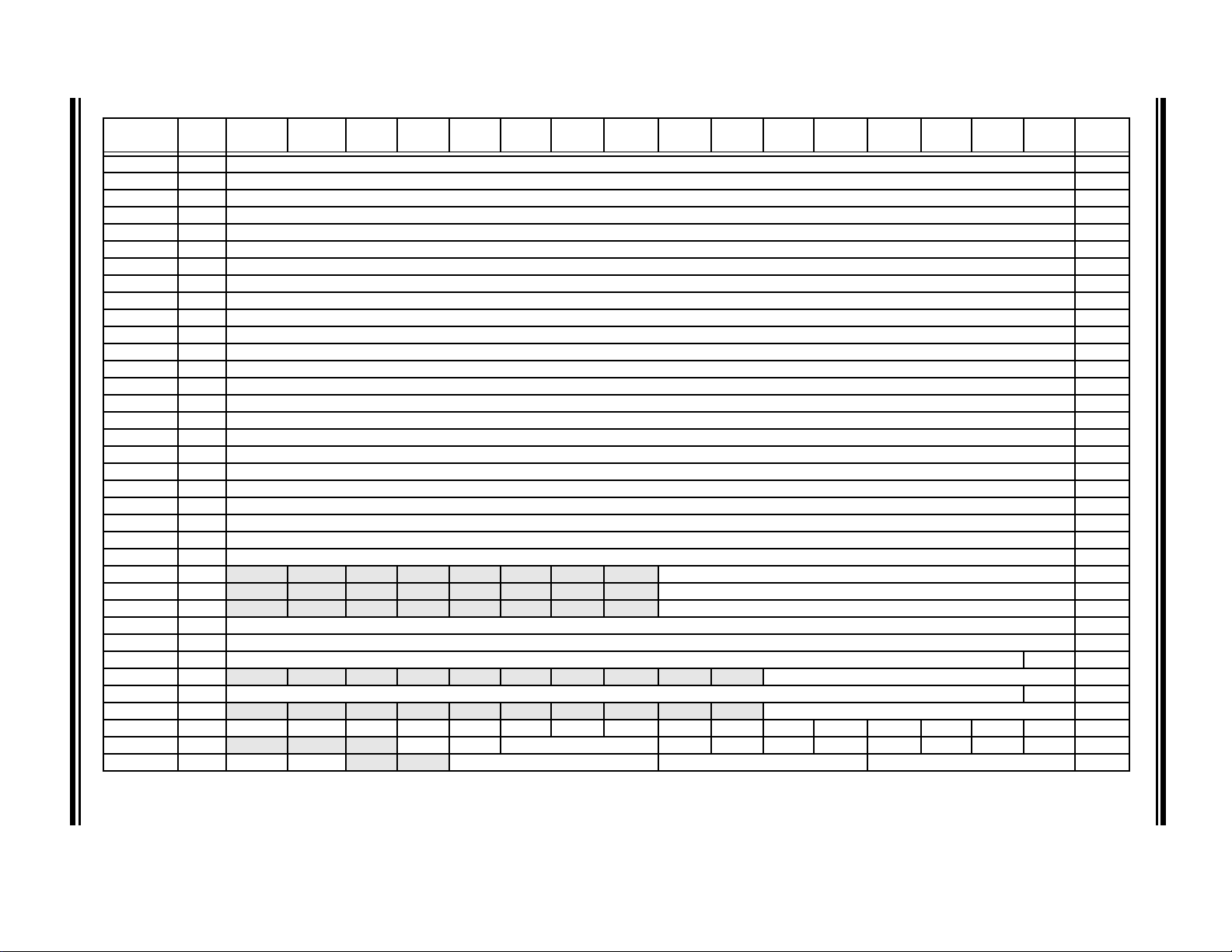
DS70652E-page 56 2011-2012 Microchip Technology Inc.
TABLE 4-1: CPU CORE REGISTER MAP
SFR Name
WREG0 0000 Working Register 0 xxxx
WREG1 0002 Working Register 1 xxxx
WREG2 0004 Working Register 2 xxxx
WREG3 0006 Working Register 3 xxxx
WREG4 0008 Working Register 4 xxxx
WREG5 000A Working Register 5 xxxx
WREG6 000C Working Register 6 xxxx
WREG7 000E Working Register 7 xxxx
WREG8 0010 Working Register 8 xxxx
WREG9 0012 Working Register 9 xxxx
WREG10 0014 Working Register 10 xxxx
WREG11 0016 Working Register 11 xxxx
WREG12 0018 Working Register 12 xxxx
WREG13 001A Working Register 13 xxxx
WREG14 001C Working Register 14 xxxx
WREG15 001E Working Register 15 0800
SPLIM 0020 Stack Pointer Limit Register xxxx
ACCAL 0022 Accumulator A Low Word Register xxxx
ACCAH 0024 Accumulator A High Word Register xxxx
ACCAU 0026 Accumulator A Upper Word Register xxxx
ACCBL 0028 Accumulator B Low Word Register xxxx
ACCBH 002A Accumulator B High Word Register xxxx
ACCBU 002C Accumulator B Upper Word Register xxxx
PCL 002E Program Counter Low Word Register 0000
PCH 0030
TBLPAG 0032
PSVPAG 0034
RCOUNT 0036 Repeat Loop Counter Register xxxx
DCOUNT 0038 DCOUNT<15:0> xxxx
DOSTARTL 003A DOSTARTL<15:1> 0xxxx
DOSTARTH 003C
DOENDL 003E DOENDL<15:1> 0xxxx
DOENDH 0040
SR 0042 OA OB SA SB OAB SAB DA DC IPL2 IPL1 IPL0 RA N OV Z C 0000
CORCON 0044
MODCON 0046 XMODEN YMODEN
Legend: x = unknown value on Reset, — = unimplemented, read as ‘0’. Reset values are shown in hexadecimal.
SFR
Addr
Bit 15 Bit 14 Bit 13 Bit 12 Bit 11 Bit 10 Bit 9 Bit 8 Bit 7 Bit 6 Bit 5 Bit 4 Bit 3 Bit 2 Bit 1 Bit 0
— — — — — — — — Program Counter High Byte Register 0000
— — — — — — — — Table Page Address Pointer Register 0000
— — — — — — — — Program Memory Visibility Page Address Pointer Register 0000
— — — — — — — — — — DOSTARTH<5:0> 00xx
— — — — — — — — — — DOENDH 00xx
— — — US EDT DL<2:0> SATA SATB SATDW ACCSAT IPL3 PSV RND IF 0020
— — BWM<3:0> YWM<3:0> XWM<3:0> 0000
All
Resets
dsPIC33FJ16(GP/MC)101/102 AND dsPIC33FJ32(GP/MC)101/102/104
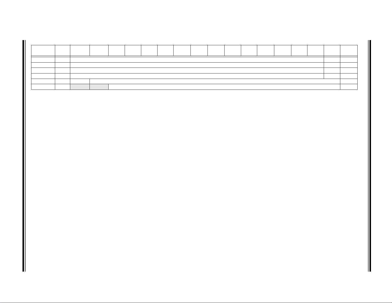
2011-2012 Microchip Technology Inc. DS70652E-page 57
TABLE 4-1: CPU CORE REGISTER MAP (CONTINUED)
SFR Name
XMODSRT 0048 XS<15:1> 0xxxx
XMODEND 004A XE<15:1> 1xxxx
YMODSRT 004C YS<15:1> 0xxxx
YMODEND 004E YE<15:1> 1xxxx
XBREV 0050 BREN XB<14:0> xxxx
DISICNT 0052
Legend: x = unknown value on Reset, — = unimplemented, read as ‘0’. Reset values are shown in hexadecimal.
SFR
Addr
Bit 15 Bit 14 Bit 13 Bit 12 Bit 11 Bit 10 Bit 9 Bit 8 Bit 7 Bit 6 Bit 5 Bit 4 Bit 3 Bit 2 Bit 1 Bit 0
— — Disable Interrupts Counter Register 0000
All
Resets
dsPIC33FJ16(GP/MC)101/102 AND dsPIC33FJ32(GP/MC)101/102/104
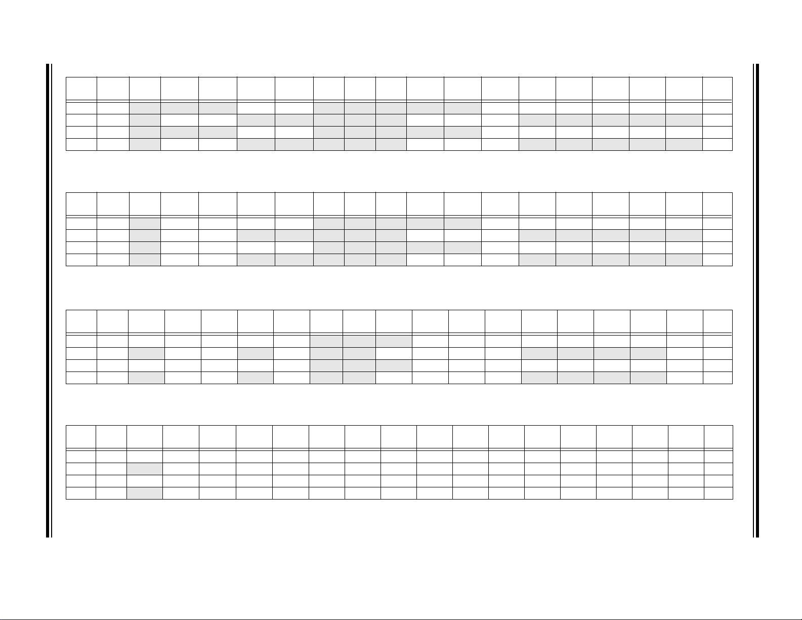
DS70652E-page 58 2011-2012 Microchip Technology Inc.
TABLE 4-2: CHANGE NOTIFICATION REGISTER MAP FOR dsPIC33FJXXGP101 DEVICES
SFR
Name
CNEN1 0060
CNEN2 0062
CNPU1 0068
CNPU2 006A
Legend: x = unknown value on Reset, — = unimplemented, read as ‘0’. Reset values are shown in hexadecimal.
SFR
Bit 15 Bit 14 Bit 13 Bit 12 Bit 11 Bit 10 Bit 9 Bit 8 Bit 7 Bit 6 Bit 5 Bit 4 Bit 3 Bit 2 Bit 1 Bit 0
Addr
— — — CN12IE CN11IE — — — — — CN5IE CN4IE CN3IE CN2IE CN1IE CN0IE 0000
— CN30IE CN29IE — — — — — CN23IE CN22IE CN21IE — — — — — 0000
— — — CN12PUE CN11PUE — — — — — CN5PUE CN4PUE CN3PUE CN2PUE CN1PUE CN0PUE 0000
— CN30PUE CN29PUE — — — — — CN23PUE CN22PUE CN21PUE — — — — — 0000
TABLE 4-3: CHANGE NOTIFICATION REGISTER MAP FOR dsPIC33FJXXMC101 DEVICES
SFR
Name
CNEN1 0060
CNEN2 0062
CNPU1 0068
CNPU2 006A
Legend: x = unknown value on Reset, — = unimplemented, read as ‘0’. Reset values are shown in hexadecimal.
SFR
Bit 15 Bit 14 Bit 13 Bit 12 Bit 11 Bit 10 Bit 9 Bit 8 Bit 7 Bit 6 Bit 5 Bit 4 Bit 3 Bit 2 Bit 1 Bit 0
Addr
— CN14IE CN13IE CN12IE CN11IE — — — — — CN5IE CN4IE CN3IE CN2IE CN1IE CN0IE 0000
— CN30IE CN29IE — — — — — CN23IE CN22IE CN21IE — — — — — 0000
— CN14PUE CN13PUE CN12PUE CN11PUE — — — — — CN5PUE CN4PUE CN3PUE CN2PUE CN1PUE CN0PUE 0000
— CN30PUE CN29PUE — — — — — CN23PUE CN22PUE CN21PUE — — — — — 0000
TABLE 4-4: CHANGE NOTIFICATION REGISTER MAP FOR dsPIC33FJXX(GP/MC)102 DEVICES
SFR
Name
CNEN1 0060 CN15IE CN14IE CN13IE CN12IE CN11IE
CNEN2 0062
CNPU1 0068 CN15PUE CN14PUE CN13PUE CN12PUE CN11PUE
CNPU2 006A
Legend: x = unknown value on Reset, — = unimplemented, read as ‘0’. Reset values are shown in hexadecimal.
SFR
Addr
Bit 15 Bit 14 Bit 13 Bit 12 Bit 11 Bit 10 Bit 9 Bit 8 Bit 7 Bit 6 Bit 5 Bit 4 Bit 3 Bit 2 Bit 1 Bit 0
— — — CN7IE CN6IE CN5IE CN4IE CN3IE CN2IE CN1IE CN0IE 0000
— CN30IE CN29IE —CN27IE— — CN24IE CN23IE CN22IE CN21IE — — — —CN16IE0000
— — — CN7PUE CN6PUE CN5PUE CN4PUE CN3PUE CN2PUE CN1PUE CN0PUE 0000
— CN30PUE CN29PUE — CN27PUE — — CN24PUE CN23PUE CN22PUE CN21PUE — — — — CN16PUE 0000
All
Resets
All
Resets
All
Resets
dsPIC33FJ16(GP/MC)101/102 AND dsPIC33FJ32(GP/MC)101/102/104
TABLE 4-5: CHANGE NOTIFICATION REGISTER MAP FOR dsPIC33FJ32(GP/MC)104 DEVICES
SFR
Name
CNEN1 0060 CN15IE CN13IE CN13IE CN12IE CN11IE CN10IE CN9IE CN8IE CN7IE CN6IE CN5IE CN4IE CN3IE CN2IE CN1IE CN0IE 0000
CNEN2 0062
CNPU1 0068 CN15PUE CN13PUE CN13PUE CN12PUE CN11PUE CN10PUE CN9PUE CN8PUE CN7PUE CN6PUE CN5PUE CN4PUE CN3PUE CN2PUE CN1PUE CN0PUE 0000
CNPU2 006A
Legend: x = unknown value on Reset, — = unimplemented, read as ‘0’. Reset values are shown in hexadecimal.
SFR
Addr
Bit 15 Bit 14 Bit 13 Bit 12 Bit 11 Bit 10Bit 9Bit 8Bit 7Bit 6Bit 5Bit 4Bit 3Bit 2Bit 1Bit 0
— CN30IE CN29IE CN28IE CN27IE CN26IE CN25IE CN24IE CN23IE CN22IE CN21IE CN20IE CN19IE CN18IE CN17IE CN16IE 0000
— CN30PUE CN29PUE CN28PUE CN27PUE CN26PUE CN25PUE CN24PUE CN23PUE CN22PUE CN21PUE CN20PUE CN19PUE CN18PUE CN17PUE CN16PUE 0000
All
Resets

2011-2012 Microchip Technology Inc. DS70652E-page 59
TABLE 4-6: INTERRUPT CONTROLLER REGISTER MAP
SFR
SFR
Name
INTCON1 0080 NSTDIS OVAERR OVBERR COVAERR COVBERR OVATE OVBTE COVTE SFTACERR DIV0ERR
INTCON2 0082 ALTIVT DISI
IFS0 0084
IFS1 0086
IFS2 0088
IFS3 008A FLTA1IF
IFS4 008C
IEC0 0094
IEC1 0096
IEC2 0098
IEC3 009A FLTA1IE
IEC4 009C
IPC0 00A4
IPC1 00A6
IPC2 00A8
IPC3 00AA
IPC4 00AC
IPC5 00AE
IPC6 00B0
IPC7 00B2
IPC9 00B6
IPC14 00C0
IPC15 00C2
IPC16 00C4
IPC19 00CA
INTTREG 00E0
Legend: x = unknown value on Reset, — = unimplemented, read as ‘0’. Reset values are shown in hexadecimal.
Note 1: This bit is available in dsPIC33FJXXMC10X devices only.
2: This bit is available in dsPIC33FJ32(GP/MC)10X devices only.
3: This bit is available in dsPIC33FJ(16/32)MC102/104 devices only.
Bit 15 Bit 14 Bit 13 Bit 12 Bit 11 Bit 10 Bit 9 Bit 8 Bit 7 Bit 6 Bit 5 Bit 4 Bit 3 Bit 2 Bit 1 Bit 0
Addr
— — — — — — — — — — — INT2EP INT1EP INT0EP 0000
— — AD1IF U1TXIF U1RXIF SPI1IF SPI1EIF T3IF T2IF OC2IF IC2IF — T1IF OC1IF IC1IF INT0IF 0000
— —INT2IFT5IF
(2)
T4IF
(2)
— — — — — — INT1IF CNIF CMIF MI2C1IF SI2C1IF 0000
— — — — — — — — — —IC3IF — — — — — 0000
(1)
RTCIF — — — —PWM1IF
(1)
— — — — — — — — — 0000
— —CTMUIF — — — — — — — — — — — U1EIF FLTB1IF
— — AD1IE U1TXIE U1RXIE SPI1IE SPI1EIE T3IE T2IE OC2IE IC2IE — T1IE OC1IE IC1IE INT0IE 0000
— — INT2IE T5IE
(2)
T4IE
(2)
— — — — — — INT1IE CNIE CMIE MI2C1IE SI2C1IE 0000
— — — — — — — — — —IC3IE — — — — — 0000
(1)
RTCIE — — — —PWM1IE
(1)
— — — — — — — — — 0000
— —CTMUIE — — — — — — — — — — — U1EIE FLTB1IE
— T1IP<2:0> —OC1IP<2:0> —IC1IP<2:0>— INT0IP<2:0> 4444
— T2IP<2:0> —OC2IP<2:0> —IC2IP<2:0>— — — — 4440
— U1RXIP<2:0> — SPI1IP<2:0> — SPI1EIP<2:0> — T3IP<2:0> 4444
— — — — — — — — —AD1IP<2:0>— U1TXIP<2:0> 0044
— CNIP<2:0> — CMIP<2:0> — MI2C1IP<2:0> — SI2C1IP<2:0> 4444
— — — — — — — — — — — — — INT1IP<2:0> 0004
— T4IP<2:0>
(2)
— — — — — — — — — — — — 4000
— — — — — — — — — INT2IP<2:0> — T5IP<2:0>
— — — — — — — — —IC3IP<2:0>— — — — 0040
— — — — — — — — — PWM1IP<2:0>
— FLTA1IP<2:0>
(1)
— RTCIP<2:0> — — — — — — — — 4400
— — — — — — — — —U1EIP<2:0>— FLTB1IP<2:0>
— — — — — — — — — CTMUIP<2:0> — — — — 0040
— — — —ILR<3:0> — VECNUM<6:0> 0000
All
Resets
— MATHERR ADDRERR STKERR OSCFAIL — 0000
(3)
0000
(3)
0000
(2)
(1)
— — — — 0040
(3)
0044
0040
dsPIC33FJ16(GP/MC)101/102 AND dsPIC33FJ32(GP/MC)101/102/104

DS70652E-page 60 2011-2012 Microchip Technology Inc.
TABLE 4-7: TIMERS REGISTER MAP FOR dsPIC33FJ16(GP/MC)10X DEVICES
SFR
SFR
Name
TMR1 0100 Timer1 Register 0000
PR1 0102 Period Register 1 FFFF
T1CON 0104 TON
TMR2 0106 Timer2 Register 0000
TMR3HLD 0108 Timer3 Holding Register (for 32-bit timer operations only) xxxx
TMR3 010A Timer3 Register 0000
PR2 010C Period Register 2 FFFF
PR3 010E Period Register 3 FFFF
T2CON 0110 TON
T3CON 0112 TON
Legend: x = unknown value on Reset, — = unimplemented, read as ‘0’. Reset values are shown in hexadecimal.
Bit 15 Bit 14 Bit 13 Bit 12 Bit 11 Bit 10 Bit 9 Bit 8 Bit 7 Bit 6 Bit 5 Bit 4 Bit 3 Bit 2 Bit 1 Bit 0
Addr
—TSIDL— — — — — — TGATE TCKPS<1:0> —TSYNCTCS — 0000
—TSIDL— — — — — — TGATE TCKPS<1:0> T32 —TCS— 0000
—TSIDL— — — — — — TGATE TCKPS<1:0> — —TCS— 0000
All
Resets
TABLE 4-8: TIMERS REGISTER MAP FOR DSPIC33FJ32(GP/MC)10X DEVICES
SFR
SFR
Name
TMR1 0100 Timer1 Register 0000
PR1 0102 Period Register 1 FFFF
T1CON 0104 TON
TMR2 0106 Timer2 Register 0000
TMR3HLD 0108 Timer3 Holding Register (for 32-bit timer operations only) xxxx
TMR3 010A Timer3 Register 0000
PR2 010C Period Register 2 FFFF
PR3 010E Period Register 3 FFFF
T2CON 0110 TON
T3CON 0112 TON
TMR4 0114 Timer4 Register 0000
TMR5HLD 0116 Timer5 Holding Register (for 32-bit operations only) xxxx
TMR5 0118 Timer5 Register 0000
PR4 011A Period Register 4 FFFF
PR5 011C Period Register 5 FFFF
T4CON 011E TON
T5CON 0120 TON
Legend: x = unknown value on Reset, — = unimplemented, read as ‘0’. Reset values are shown in hexadecimal.
Bit 15 Bit 14 Bit 13 Bit 12 Bit 11 Bit 10 Bit 9 Bit 8 Bit 7 Bit 6 Bit 5 Bit 4 Bit 3 Bit 2 Bit 1 Bit 0
Addr
—TSIDL— — — — — — TGATE TCKPS<1:0> —TSYNCTCS — 0000
—TSIDL— — — — — — TGATE TCKPS<1:0> T32 —TCS— 0000
—TSIDL— — — — — — TGATE TCKPS<1:0> — —TCS— 0000
—TSIDL— — — — — — TGATE TCKPS<1:0> T32 —TCS— 0000
—TSIDL— — — — — — TGATE TCKPS<1:0> — —TCS— 0000
All
Resets
dsPIC33FJ16(GP/MC)101/102 AND dsPIC33FJ32(GP/MC)101/102/104

2011-2012 Microchip Technology Inc. DS70652E-page 61
TABLE 4-9: INPUT CAPTURE REGISTER MAP
SFR Name
IC1BUF 0140 Input 1 Capture Register xxxx
IC1CON 0142
IC2BUF 0144 Input 2 Capture Register xxxx
IC2CON 0146
IC3BUF 0148 Input 3 Capture Register xxxx
IC3CON 014A
Legend: x = unknown value on Reset, — = unimplemented, read as ‘0’. Reset values are shown in hexadecimal.
SFR
Addr
Bit 15 Bit 14 Bit 13 Bit 12 Bit 11 Bit 10 Bit 9 Bit 8 Bit 7 Bit 6 Bit 5 Bit 4 Bit 3 Bit 2 Bit 1 Bit 0 All Resets
— —ICSIDL— — — — — ICTMR ICI<1:0> ICOV ICBNE ICM<2:0> 0000
— —ICSIDL— — — — — ICTMR ICI<1:0> ICOV ICBNE ICM<2:0> 0000
— —ICSIDL— — — — — ICTMR ICI<1:0> ICOV ICBNE ICM<2:0> 0000
TABLE 4-10: OUTPUT COMPARE REGISTER MAP
SFR Name
OC1RS 0180 Output Compare 1 Secondary Register xxxx
OC1R 0182 Output Compare 1 Register xxxx
OC1CON 0184 — —OCSIDL— — — — — — — — OCFLT OCTSEL OCM<2:0> 0000
OC2RS 0186 Output Compare 2 Secondary Register xxxx
OC2R 0188 Output Compare 2 Register xxxx
OC2CON 018A
Legend: x = unknown value on Reset, — = unimplemented, read as ‘0’. Reset values are shown in hexadecimal.
SFR
Addr
Bit 15 Bit 14 Bit 13 Bit 12 Bit 11 Bit 10 Bit 9 Bit 8 Bit 7 Bit 6 Bit 5 Bit 4 Bit 3 Bit 2 Bit 1 Bit 0
— —OCSIDL— — — — — — — — OCFLT OCTSEL OCM<2:0> 0000
TABLE 4-11: 6-OUTPUT PWM1 REGISTER MAP FOR dsPIC33FJXXMC10X DEVICES
SFR Name Addr. Bit 15 Bit 14 Bit 13 Bit 12 Bit 11 Bit 10 Bit 9 Bit 8 Bit 7 Bit 6 Bit 5 Bit 4 Bit 3 Bit 2 Bit 1 Bit 0 Reset State
P1TCON 01C0 PTEN
P1TMR 01C2 PTDIR PWM Timer Count Value Register
P1TPER 01C4 — PWM Time Base Period Register
P1SECMP 01C6 SEVTDIR PWM Special Event Compare Register
PWM1CON1
PWM1CON2
P1DTCON1 01CC DTBPS<1:0> DTB<5:0> DTAPS<1:0> DTA<5:0>
P1DTCON2 01CE — — — — — — — — — — DTS3A DTS3I DTS2A DTS2I DTS1A DTS1I
P1FLTACON 01D0 — — FAOV3H FAOV3L FAOV2H FAOV2L FAOV1H FAOV1L FLTAM — — — — FAEN3 FAEN2 FAEN1
P1FLTBCON 01D2 — — FBOV3H FBOV3L FBOV2H FBOV2L FBOV1H FBOV1L FLTBM — — — — FBEN3 FBEN2 FBEN1
P1OVDCON 01D4 — — POVD3H POVD3L POVD2H POVD2L POVD1H POVD1L — — POUT3H POUT3L POUT2H POUT2L POUT1H POUT1L
P1DC1 01D6 PWM Duty Cycle 1 Register
P1DC2 01D8 PWM Duty Cycle 2 Register
P1DC3 01DA PWM Duty Cycle 3 Register
PWM1KEY 01DE PWMKEY <15:0>
Legend: — = unimplemented, read as ‘0’
01C8 — — — — —PMOD3PMOD2PMOD1— PEN3H PEN2H PEN1H — PEN3L PEN2L PEN1L
01CA — — — —SEVOPS<3:0>— — — — — IUE OSYNC UDIS
—PTSIDL — — — — — PTOPS<3:0> PTCKPS<1:0> PTMOD<1:0>
dsPIC33FJ16(GP/MC)101/102 AND dsPIC33FJ32(GP/MC)101/102/104
All
Resets
0000 0000 0000 0000
0000 0000 0000 0000
0111 1111 1111 1111
0000 0000 0000 0000
0000 0000 0000 0000
0000 0000 0000 0000
0000 0000 0000 0000
0000 0000 0000 0000
0000 0000 0000 0111
0000 0000 0000 0111
0011 1111 0000 0000
0000 0000 0000 0000
0000 0000 0000 0000
0000 0000 0000 0000
0000 0000 0000 0000
DS70652E-page 62 2011-2012 Microchip Technology Inc.
TABLE 4-12: I2C1 REGISTER MAP
SFR Name
I2C1RCV 0200
I2C1TRN 0202
I2C1BRG 0204
I2C1CON 0206 I2CEN
I2C1STAT 0208 ACKSTAT TRSTAT
I2C1ADD 020A
I2C1MSK 020C
Legend: x = unknown value on Reset, — = unimplemented, read as ‘0’. Reset values are shown in hexadecimal.
SFR
Addr
Bit 15Bit 14Bit 13Bit 12Bit 11Bit 10Bit 9Bit 8Bit 7Bit 6Bit 5Bit 4Bit 3Bit 2Bit 1Bit 0
— — — — — — — — Receive Register 0000
— — — — — — — — Transmit Register 00FF
— — — — — — — Baud Rate Generator Register 0000
— I2CSIDL SCLREL IPMIEN A10M DISSLW SMEN GCEN STREN ACKDT ACKEN RCEN PEN RSEN SEN 1000
— — — BCL GCSTAT ADD10 IWCOL I2COV D_A P S R_W RBF TBF 0000
— — — — — — Address Register 0000
— — — — — — Address Mask Register 0000
Resets
TABLE 4-13: UART1 REGISTER MAP
SFR Name
U1MODE 0220 UARTEN
U1STA 0222 UTXISEL1 UTXINV UTXISEL0
U1TXREG 0224
U1RXREG 0226
U1BRG 0228 Baud Rate Generator Prescaler 0000
Legend: x = unknown value on Reset, — = unimplemented, read as ‘0’. Reset values are shown in hexadecimal.
SFR
Addr
Bit 15 Bit 14 Bit 13 Bit 12 Bit 11 Bit 10 Bit 9 Bit 8 Bit 7 Bit 6 Bit 5 Bit 4 Bit 3 Bit 2 Bit 1 Bit 0
— USIDL IREN RTSMD — UEN1 UEN0 WAKE LPBACK ABAUD URXINV BRGH PDSEL<1:0> STSEL 0000
— UTXBRK UTXEN UTXBF TRMT URXISEL<1:0> ADDEN RIDLE PERR FERR OERR URXDA 0110
— — — — — — — UART Transmit Register xxxx
— — — — — — — UART Receive Register 0000
All
Resets
dsPIC33FJ16(GP/MC)101/102 AND dsPIC33FJ32(GP/MC)101/102/104
All
TABLE 4-14: SPI1 REGISTER MAP
SFR
Name
SPI1STAT 0240 SPIEN
SPI1CON1 0242
SPI1CON2 0244 FRMEN SPIFSD FRMPOL
SPI1BUF 0248 SPI1 Transmit and Receive Buffer Register 0000
Legend: x = unknown value on Reset, — = unimplemented, read as ‘0’. Reset values are shown in hexadecimal.
SFR
Addr
Bit 15 Bit 14 Bit 13 Bit 12 Bit 11 Bit 10 Bit 9 Bit 8 Bit 7 Bit 6 Bit 5 Bit 4 Bit 3 Bit 2 Bit 1 Bit 0
— SPISIDL — — — — — —SPIROV— — — —SPITBFSPIRBF0000
— — — DISSCK DISSDO MODE16 SMP CKE SSEN CKP MSTEN SPRE<2:0> PPRE<1:0> 0000
— — — — — — — — — — —FRMDLY— 0000
All
Resets

2011-2012 Microchip Technology Inc. DS70652E-page 63
TABLE 4-15: ADC1 REGISTER MAP FOR dsPIC33FJXX(GP/MC)101 DEVICES
File Name Addr Bit 15 Bit 14 Bit 13 Bit 12 Bit 11 Bit 10 Bit 9 Bit 8 Bit 7 Bit 6 Bit 5 Bit 4 Bit 3 Bit 2 Bit 1 Bit 0
ADC1BUF0 0300 ADC Data Buffer 0 xxxx
ADC1BUF1 0302 ADC Data Buffer 1 xxxx
ADC1BUF2 0304 ADC Data Buffer 2 xxxx
ADC1BUF3 0306 ADC Data Buffer 3 xxxx
ADC1BUF4 0308 ADC Data Buffer 4 xxxx
ADC1BUF5 030A ADC Data Buffer 5 xxxx
ADC1BUF6 030C ADC Data Buffer 6 xxxx
ADC1BUF7 030E ADC Data Buffer 7 xxxx
ADC1BUF8 0310 ADC Data Buffer 8 xxxx
ADC1BUF9 0312 ADC Data Buffer 9 xxxx
ADC1BUFA 0314 ADC Data Buffer 10 xxxx
ADC1BUFB 0316 ADC Data Buffer 11 xxxx
ADC1BUFC 0318 ADC Data Buffer 12 xxxx
ADC1BUFD 031A ADC Data Buffer 13 xxxx
ADC1BUFE 031C ADC Data Buffer 14 xxxx
ADC1BUFF 031E ADC Data Buffer 15 xxxx
AD1CON1 0320 ADON
AD1CON2 0322 VCFG<2:0>
AD1CON3 0324 ADRC
AD1CHS123 0326
AD1CHS0 0328 CH0NB
AD1PCFGL 032C
AD1CSSL 0330
Legend: x = unknown value on Reset, — = unimplemented, read as ‘0’. Reset values are shown in hexadecimal.
Note 1: This bit is available in dsPIC33FJ32(GP/MC)101/102 devices only.
— — — — — CH123NB<1:0> CH123SB — — — — — CH123NA<1:0> CH123SA 0000
— — — — —PCFG10
— — — — — CSS10
—ADSIDL — — — FORM<1:0> SSRC<2:0> — SIMSAM ASAM SAMP DONE 0000
— — CSCNA CHPS<1:0> BUFS — SMPI<3:0> BUFM ALTS 0000
— — SAMC<4:0> ADCS<7:0> 0000
— — CH0SB<4:0> CH0NA — — CH0SA<4:0> 0000
(1)
(1)
PCFG9
CSS9
(1)
— — — — — PCFG3 PCFG2 PCFG1 PCFG0 0000
(1)
— — — — — CSS3 CSS2 CSS1 CSS0 0000
Resets
All
dsPIC33FJ16(GP/MC)101/102 AND dsPIC33FJ32(GP/MC)101/102/104

DS70652E-page 64 2011-2012 Microchip Technology Inc.
TABLE 4-16: ADC1 REGISTER MAP FOR dsPIC33FJXX(GP/MC)102 DEVICES
File Name Addr Bit 15 Bit 14 Bit 13 Bit 12 Bit 11 Bit 10 Bit 9 Bit 8 Bit 7 Bit 6 Bit 5 Bit 4 Bit 3 Bit 2 Bit 1 Bit 0
ADC1BUF0 0300 ADC Data Buffer 0 xxxx
ADC1BUF1 0302 ADC Data Buffer 1 xxxx
ADC1BUF2 0304 ADC Data Buffer 2 xxxx
ADC1BUF3 0306 ADC Data Buffer 3 xxxx
ADC1BUF4 0308 ADC Data Buffer 4 xxxx
ADC1BUF5 030A ADC Data Buffer 5 xxxx
ADC1BUF6 030C ADC Data Buffer 6 xxxx
ADC1BUF7 030E ADC Data Buffer 7 xxxx
ADC1BUF8 0310 ADC Data Buffer 8 xxxx
ADC1BUF9 0312 ADC Data Buffer 9 xxxx
ADC1BUFA 0314 ADC Data Buffer 10 xxxx
ADC1BUFB 0316 ADC Data Buffer 11 xxxx
ADC1BUFC 0318 ADC Data Buffer 12 xxxx
ADC1BUFD 031A ADC Data Buffer 13 xxxx
ADC1BUFE 031C ADC Data Buffer 14 xxxx
ADC1BUFF 031E ADC Data Buffer 15 xxxx
AD1CON1 0320 ADON
AD1CON2 0322 VCFG<2:0>
AD1CON3 0324 ADRC
AD1CHS123 0326
AD1CHS0 0328 CH0NB
AD1PCFGL 032C
AD1CSSL 0330
Legend: x = unknown value on Reset, — = unimplemented, read as ‘0’. Reset values are shown in hexadecimal.
Note 1: This bit is available in dsPIC33FJ32(GP/MC)101/102 devices only.
— — — — — CH123NB<1:0> CH123SB — — — — — CH123NA<1:0> CH123SA 0000
— — — — —PCFG10
— — — — — CSS10
—ADSIDL — — — FORM<1:0> SSRC<2:0> — SIMSAM ASAM SAMP DONE 0000
— — CSCNA CHPS<1:0> BUFS — SMPI<3:0> BUFM ALTS 0000
— — SAMC<4:0> ADCS<7:0> 0000
— — CH0SB<4:0> CH0NA — — CH0SA<4:0> 0000
(1)
(1)
PCFG9
CSS9
(1)
— — — PCFG5 PCFG4 PCFG3 PCFG2 PCFG1 PCFG0 0000
(1)
— — — CSS5 CSS4 CSS3 CSS2 CSS1 CSS0 0000
Resets
dsPIC33FJ16(GP/MC)101/102 AND dsPIC33FJ32(GP/MC)101/102/104
All

2011-2012 Microchip Technology Inc. DS70652E-page 65
TABLE 4-17: ADC1 REGISTER MAP FOR dsPIC33FJ32(GP/MC)104 DEVICES
File Name Addr Bit 15 Bit 14 Bit 13 Bit 12 Bit 11 Bit 10 Bit 9 Bit 8 Bit 7 Bit 6 Bit 5 Bit 4 Bit 3 Bit 2 Bit 1 Bit 0
ADC1BUF0 0300 ADC Data Buffer 0 xxxx
ADC1BUF1 0302 ADC Data Buffer 1 xxxx
ADC1BUF2 0304 ADC Data Buffer 2 xxxx
ADC1BUF3 0306 ADC Data Buffer 3 xxxx
ADC1BUF4 0308 ADC Data Buffer 4 xxxx
ADC1BUF5 030A ADC Data Buffer 5 xxxx
ADC1BUF6 030C ADC Data Buffer 6 xxxx
ADC1BUF7 030E ADC Data Buffer 7 xxxx
ADC1BUF8 0310 ADC Data Buffer 8 xxxx
ADC1BUF9 0312 ADC Data Buffer 9 xxxx
ADC1BUFA 0314 ADC Data Buffer 10 xxxx
ADC1BUFB 0316 ADC Data Buffer 11 xxxx
ADC1BUFC 0318 ADC Data Buffer 12 xxxx
ADC1BUFD 031A ADC Data Buffer 13 xxxx
ADC1BUFE 031C ADC Data Buffer 14 xxxx
ADC1BUFF 031E ADC Data Buffer 15 xxxx
AD1CON1 0320 ADON
AD1CON2 0322 VCFG<2:0>
AD1CON3 0324 ADRC
AD1CHS123 0326
AD1CHS0 0328 CH0NB
AD1PCFGL 032C PCFG15
AD1CSSL 0330 CSS15
Legend: x = unknown value on Reset, — = unimplemented, read as ‘0’. Reset values are shown in hexadecimal.
Note 1: This bit is available in dsPIC33FJ32(GP/MC)104 devices only.
— — — — — CH123NB<1:0> CH123SB — — — — — CH123NA<1:0> CH123SA 0000
—ADSIDL — — — FORM<1:0> SSRC<2:0> — SIMSAM ASAM SAMP DONE 0000
— — CSCNA CHPS<1:0> BUFS —SMPI<3:0>BUFMALTS0000
— — SAMC<4:0> ADCS<7:0> 0000
— — CH0SB<4:0> CH0NA — — CH0SA<4:0> 0000
— — PCFG12 PCFG11 PCFG10
— — CSS12 CSS11 CSS10
(1)
(1)
PCFG9
CSS9
(1)
PCFG8 PCFG7 PCFG6 PCFG5 PCFG4 PCFG3 PCFG2 PCFG1 PCFG0 0000
(1)
CSS8 CSS7 CSS6 CSS5 CSS4 CSS3 CSS2 CSS1 CSS0 0000
Resets
dsPIC33FJ16(GP/MC)101/102 AND dsPIC33FJ32(GP/MC)101/102/104
All

DS70652E-page 66 2011-2012 Microchip Technology Inc.
TABLE 4-18: CTMU REGISTER MAP
File Name Addr Bit 15 Bit 14 Bit 13 Bit 12 Bit 11 Bit 10 Bit 9 Bit 8 Bit 7 Bit 6 Bit 5 Bit 4 Bit 3 Bit 2 Bit 1 Bit 0
CTMUCON1 033A CTMUEN
CTMUCON2 033C EDG1MOD EDG1POL EDG1SEL<3:0> EDG2STAT EDG1STAT EDG2MOD EDG2POL EDG2SEL<3:0>
CTMUICON 033E ITRIM<5:0> IRNG<1:0>
Legend: x = unknown value on Reset, — = unimplemented, read as ‘0’. Reset values are shown in hexadecimal.
— CTMUSIDL TGEN EDGEN EDGSEQEN IDISSEN CTTRIG — — — — — — — — 0000
— — 0000
— — — — — — — — 0000
All
Resets
TABLE 4-19: REAL-TIME CLOCK AND CALENDAR REGISTER MAP
File Name Addr Bit 15 Bit 14 Bit 13 Bit 12 Bit 11 Bit 10 Bit 9 Bit 8 Bit 7 Bit 6 Bit 5 Bit 4 Bit 3 Bit 2 Bit 1 Bit 0
ALRMVAL 0620 Alarm Value Register Window based on APTR<1:0> xxxx
ALCFGRPT 0622 ALRMEN CHIME AMASK<3:0> ALRMPTR<1:0> ARPT<7:0> 0000
RTCVAL 0624 RTCC Value Register Window based on RTCPTR<1:0> xxxx
RCFGCAL 0626 RTCEN
Legend: x = unknown value on Reset, — = unimplemented, read as ‘0’. Reset values are shown in hexadecimal.
— RTCWREN RTCSYNC HALFSEC RTCOE RTCPTR<1:0> CAL<7:0> 0000
All
Resets
TABLE 4-20: PAD CONFIGURATION REGISTER MAP
File Name Addr Bit 15 Bit 14 Bit 13 Bit 12 Bit 11 Bit 10 Bit 9 Bit 8 Bit 7 Bit 6 Bit 5 Bit 4 Bit 3 Bit 2 Bit 1 Bit 0
PADCFG1 02FC
Legend: x = unknown value on Reset, — = unimplemented, read as ‘0’. Reset values are shown in hexadecimal.
— — — — — — — — — — — — — — RTSECSEL — 0000
All
Resets
dsPIC33FJ16(GP/MC)101/102 AND dsPIC33FJ32(GP/MC)101/102/104

2011-2012 Microchip Technology Inc. DS70652E-page 67
TABLE 4-21: COMPARATOR REGISTER MAP
File Name Addr. Bit 15 Bit 14 Bit 13 Bit 12 Bit 11 Bit 10 Bit 9 Bit 8 Bit 7 Bit 6 Bit 5 Bit 4 Bit 3 Bit 2 Bit 1 Bit 0
CMSTAT 0650 CMSIDL
CVRCON 0652
CM1CON 0654 CON COE CPOL
CM1MSKSRC 0656
CM1MSKCON 0658 HLMS
CM1FLTR 065A
CM2CON 065C CON COE CPOL
CM2MSKSRC 065E
CM2MSKCON 0660 HLMS
CM2FLTR 0662
CM3CON 0664 CON COE CPOL
CM3MSKSRC 0666
CM3MSKCON 0668 HLMS
CM3FLTR 066A
Legend: x = unknown value on Reset, — = unimplemented, read as ‘0’. Reset values are shown in hexadecimal.
— — — — — VREFSEL BGSEL<1:0> CVREN CVROE CVRR —CVR<3:0>0000
— — — — SELSRCC<3:0> SELSRCB<3:0> SELSRCA<3:0> 0000
— — — — — — — — — CFSEL<2:0> CFLTREN CFDIV<2:0> 0000
— — — — SELSRCC<3:0> SELSRCB<3:0> SELSRCA<3:0> 0000
— — — — — — — — — CFSEL<2:0> CFLTREN CFDIV<2:0> 0000
— — — — SELSRCC<3:0> SELSRCB<3:0> SELSRCA<3:0> 0000
— — — — — — — — — CFSEL<2:0> CFLTREN CFDIV<2:0> 0000
— — — — C3EVT C2EVT C1EVT — — — — — C3OUT C2OUT C1OUT 0000
— — — CEVT COUT EVPOL<1:0> — CREF — — CCH<1:0> 0000
— OCEN OCNEN OBEN OBNEN OAEN OANEN NAGS PAGS ACEN ACNEN ABEN ABNEN AAEN AANEN 0000
— — — CEVT COUT EVPOL<1:0> — CREF — — CCH<1:0> 0000
— OCEN OCNEN OBEN OBNEN OAEN OANEN NAGS PAGS ACEN ACNEN ABEN ABNEN AAEN AANEN 0000
— — — CEVT COUT EVPOL<1:0> — CREF — — CCH<1:0> 0000
— OCEN OCNEN OBEN OBNEN OAEN OANEN NAGS PAGS ACEN ACNEN ABEN ABNEN AAEN AANEN 0000
TABLE 4-22: PERIPHERAL PIN SELECT INPUT REGISTER MAP
File
Name
RPINR0 0680
RPINR1 0682
RPINR3 0686
RPINR4 0688
RPINR7 068E
RPINR8 0690
RPINR11 0696
RPINR18 06A4
RPINR20 06A8
RPINR21 06AA
Legend: x = unknown value on Reset, — = unimplemented, read as ‘0’. Reset values are shown in hexadecimal.
Note 1: These bits are available in dsPIC33FJ32(GP/MC)10X devices only.
Addr Bit 15 Bit 14 Bit 13 Bit 12 Bit 11 Bit 10 Bit 9 Bit 8 Bit 7 Bit 6 Bit 5 Bit 4 Bit 3 Bit 2 Bit 1 Bit 0
— — — INT1R<4:0> — — — — — — — — 1F00
— — — — — — — — — — —INT2R<4:0>001F
— — —T3CKR<4:0>— — —T2CKR<4:0>1F1F
— — —T5CKR<4:0>
— — — IC2R<4:0> — — — IC1R<4:0> 1F1F
— — — — — — — — — — — IC3R<4:0> 001F
— — — — — — — — — — —OCFAR<4:0>001F
— — — U1CTSR<4:0> — — —U1RXR<4:0>1F1F
— — —SCK1R<4:0>
— — — — — — — — — — — SS1R<4:0> 001F
(1)
(1)
— — —T4CKR<4:0>
— — —SDI1R<4:0>
(1)
(1)
All
Resets
All
Resets
1F1F
1F1F
dsPIC33FJ16(GP/MC)101/102 AND dsPIC33FJ32(GP/MC)101/102/104

DS70652E-page 68 2011-2012 Microchip Technology Inc.
TABLE 4-23: PERIPHERAL PIN SELECT OUTPUT REGISTER MAP FOR dsPIC33FJXXGP101 DEVICES
File
Name
RPOR0 06C0 — — — RP1R<4:0> — — — RP0R<4:0> 0000
RPOR2 06C4
RPOR3 06C6
RPOR4 06C8
RPOR7 06CE
Legend: x = unknown value on Reset, — = unimplemented, read as ‘0’. Reset values are shown in hexadecimal.
Addr Bit 15 Bit 14 Bit 13 Bit 12 Bit 11 Bit 10 Bit 9 Bit 8 Bit 7 Bit 6 Bit 5 Bit 4 Bit 3 Bit 2 Bit 1 Bit 0 All Resets
— — — — — — — — — — — RP4R<4:0> 0000
— — —RP7R<4:0>— — — — — — — — 0000
— — —RP9R<4:0>— — — RP8R<4:0> 0000
— — — RP15R<4:0> — — —RP14R<4:0>0000
TABLE 4-24: PERIPHERAL PIN SELECT OUTPUT REGISTER MAP FOR dsPIC33FJXXMC101 DEVICES
File
Name
RPOR0 06C0 — — — RP1R<4:0> — — — RP0R<4:0> 0000
RPOR2 06C4
RPOR3 06C6
RPOR4 06C8
RPOR6 06CC
RPOR7 06CE
Legend: x = unknown value on Reset, — = unimplemented, read as ‘0’. Reset values are shown in hexadecimal.
Addr Bit 15 Bit 14 Bit 13 Bit 12 Bit 11 Bit 10 Bit 9 Bit 8 Bit 7 Bit 6 Bit 5 Bit 4 Bit 3 Bit 2 Bit 1 Bit 0 All Resets
— — — — — — — — — — — RP4R<4:0> 0000
— — —RP7R<4:0>— — — — — — — — 0000
— — —RP9R<4:0>— — — RP8R<4:0> 0000
— — — RP13R<4:0> — — —RP12R<4:0>0000
— — — RP15R<4:0> — — —RP14R<4:0>0000
TABLE 4-25: PERIPHERAL PIN SELECT OUTPUT REGISTER MAP FOR dsPIC33FJXX(GP/MC)102 DEVICES
File
Name
RPOR0 06C0 — — — RP1R<4:0> — — — RP0R<4:0> 0000
RPOR1 06C2
RPOR2 06C4
RPOR3 06C6
RPOR4 06C8
RPOR5 06CA
RPOR6 06CC
RPOR7 06CE
Legend: x = unknown value on Reset, — = unimplemented, read as ‘0’. Reset values are shown in hexadecimal.
Addr Bit 15 Bit 14 Bit 13 Bit 12 Bit 11 Bit 10 Bit 9 Bit 8 Bit 7 Bit 6 Bit 5 Bit 4 Bit 3 Bit 2 Bit 1 Bit 0
— — — RP3R<4:0> — — — RP2R<4:0> 0000
— — — RP5R<4:0> — — — RP4R<4:0> 0000
— — — RP7R<4:0> — — — RP6R<4:0> 0000
— — — RP9R<4:0> — — — RP8R<4:0> 0000
— — —RP11R<4:0>— — — RP10R<4:0> 0000
— — —RP13R<4:0>— — — RP12R<4:0> 0000
— — —RP15R<4:0>— — — RP14R<4:0> 0000
All
Resets
dsPIC33FJ16(GP/MC)101/102 AND dsPIC33FJ32(GP/MC)101/102/104
2011-2012 Microchip Technology Inc. DS70652E-page 69
TABLE 4-26: PERIPHERAL PIN SELECT OUTPUT REGISTER MAP FOR dsPIC33FJ32(GP/MC)104 DEVICES
File
Name
RPOR0 06C0 — — — RP1R<4:0> — — — RP0R<4:0> 0000
RPOR1 06C2
RPOR2 06C4
RPOR3 06C6
RPOR4 06C8
RPOR5 06CA
RPOR6 06CC
RPOR7 06CE
RPOR8 06D0 — — — RP17R<4:0> — — — RP16R<4:0> 0000
RPOR9 06D2
RPOR10 06D4
RPOR11 06D6
RPOR12 06D8
Legend: x = unknown value on Reset, — = unimplemented, read as ‘0’. Reset values are shown in hexadecimal.
Addr Bit 15 Bit 14 Bit 13 Bit 12 Bit 11 Bit 10 Bit 9 Bit 8 Bit 7 Bit 6 Bit 5 Bit 4 Bit 3 Bit 2 Bit 1 Bit 0
— — — RP3R<4:0> — — — RP2R<4:0> 0000
— — — RP5R<4:0> — — — RP4R<4:0> 0000
— — — RP7R<4:0> — — — RP6R<4:0> 0000
— — — RP9R<4:0> — — — RP8R<4:0> 0000
— — —RP11R<4:0>— — — RP10R<4:0> 0000
— — —RP13R<4:0>— — — RP12R<4:0> 0000
— — —RP15R<4:0>— — — RP14R<4:0> 0000
— — —RP19R<4:0>— — — RP18R<4:0> 0000
— — —RP21R<4:0>— — — RP20R<4:0> 0000
— — —RP23R<4:0>— — — RP22R<4:0> 0000
— — —RP25R<4:0>— — — RP24R<4:0> 0000
All
Resets
TABLE 4-27: PORTA REGISTER MAP FOR dsPIC33FJ16(GP/MC)101/102 DEVICES
File
Name
TRISA 02C0
PORTA 02C2
LATA 02C4
ODCA 02C6
Legend: x = unknown value on Reset, — = unimplemented, read as ‘0’. Reset values are shown in hexadecimal.
Addr Bit 15 Bit 14 Bit 13 Bit 12 Bit 11 Bit 10 Bit 9 Bit 8 Bit 7 Bit 6 Bit 5 Bit 4 Bit 3 Bit 2 Bit 1 Bit 0
— — — — — — — — — — — TRISA4 TRISA3 TRISA2 TRISA1 TRISA0 001F
— — — — — — — — — — — RA4 RA3 RA2 RA1 RA0 xxxx
— — — — — — — — — — — LATA4 LATA3 LATA2 LATA1 LATA0 xxxx
— — — — — — — — — — — ODCA4 ODCA3 ODCA2 — — 0000
All
Resets
dsPIC33FJ16(GP/MC)101/102 AND dsPIC33FJ32(GP/MC)101/102/104
TABLE 4-28: PORTA REGISTER MAP FOR dsPIC33FJ32(GP/MC)101/102 DEVICES
File
Name
TRISA 02C0
PORTA 02C2
LATA 02C4
ODCA 02C6
Legend: x = unknown value on Reset, — = unimplemented, read as ‘0’. Reset values are shown in hexadecimal.
Addr Bit 15 Bit 14 Bit 13 Bit 12 Bit 11 Bit 10 Bit 9 Bit 8 Bit 7 Bit 6 Bit 5 Bit 4 Bit 3 Bit 2 Bit 1 Bit 0
— — — — — — — — — — — TRISA4 TRISA3 TRISA2 TRISA1 TRISA0 001F
— — — — — — — — — — — RA4 RA3 RA2 RA1 RA0 xxxx
— — — — — — — — — — — LATA4 LATA3 LATA2 LATA1 LATA0 xxxx
— — — — — — — — — — — — ODCA3 ODCA2 — — 0000
All
Resets
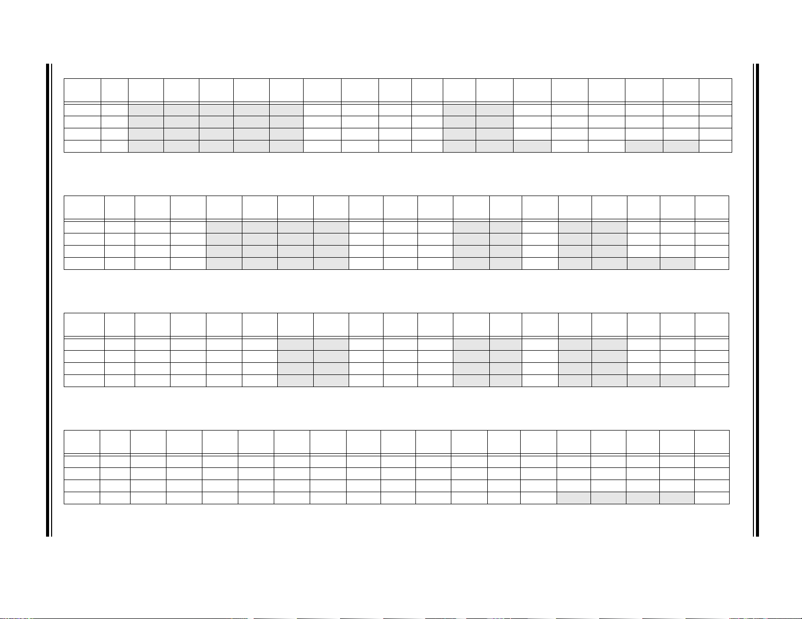
DS70652E-page 70 2011-2012 Microchip Technology Inc.
TABLE 4-29: PORTA REGISTER MAP FOR dsPIC33FJ32(GP/MC)104 DEVICES
File
Name
TRISA 02C0
PORTA 02C2
LATA 02C4
ODCA 02C6
Legend: x = unknown value on Reset, — = unimplemented, read as ‘0’. Reset values are shown in hexadecimal.
Addr Bit 15 Bit 14 Bit 13 Bit 12 Bit 11 Bit 10 Bit 9 Bit 8 Bit 7 Bit 6 Bit 5 Bit 4 Bit 3 Bit 2 Bit 1 Bit 0
— — — — — TRISA10 TRISA9 TRISA8 TRISA7 — — TRISA4 TRISA3 TRISA2 TRISA1 TRISA0 001F
— — — — — RA10 RA9 RA8 RA7 — — RA4 RA3 RA2 RA1 RA0 xxxx
— — — — — L ATA1 0 LATA 9 LATA8 LATA 7 — — LATA 4 L ATA3 L ATA2 LATA 1 LATA 0 xxxx
— — — — — ODCA10 ODCA9 ODCBA ODCA7 — — — ODCA3 ODCA2 — — 0000
TABLE 4-30: PORTB REGISTER MAP FOR dsPIC33FJ16GP101 DEVICES
File Name Addr Bit 15 Bit 14 Bit 13 Bit 12 Bit 11 Bit 10 Bit 9 Bit 8 Bit 7 Bit 6 Bit 5 Bit 4 Bit 3 Bit 2 Bit 1 Bit 0
TRISB 02C8 TRISB15 TRISB14
PORTB 02CA RB15 RB14
LATB 02CC LATB15 LATB14
ODCB 02CE ODCB15 ODCB14
Legend: x = unknown value on Reset, — = unimplemented, read as ‘0’. Reset values are shown in hexadecimal
— — — — TRISB9 TRISB8 TRISB7 — — TRISB4 — — TRISB1 TRISB0 C393
— — — — RB9 RB8 RB7 — —RB4— —RB1RB0xxxx
— — — — LATB 9 LATB 8 L ATB7 — —LATB4 — —LATB1LATB0xxxx
— — — — ODCB9 ODCB8 ODCB7 — — ODCB4 — — — — 0000
TABLE 4-31: PORTB REGISTER MAP FOR dsPIC33FJ16MC101 DEVICES
File Name Addr Bit 15 Bit 14 Bit 13 Bit 12 Bit 11 Bit 10 Bit 9 Bit 8 Bit 7 Bit 6 Bit 5 Bit 4 Bit 3 Bit 2 Bit 1 Bit 0
TRISB 02C8 TRISB15 TRISB14 TRISB13 TRISB12
PORTB 02CA RB15 RB14 RB13 RB12
LAT B 02 CC L ATB1 5 L ATB1 4 L ATB1 3 L ATB12
ODCB 02CE ODCB15 ODCB14 ODCB13 ODCB12
Legend: x = unknown value on Reset, — = unimplemented, read as ‘0’. Reset values are shown in hexadecimal
— — TRISB9 TRISB8 TRISB7 — — TRISB4 — — TRISB1 TRISB0 F393
— — RB9 RB8 RB7 — —RB4 — —RB1RB0xxxx
— — L ATB 9 LAT B8 LAT B7 — —LATB4— —LATB1LATB0xxxx
— — ODCB9 ODCB8 ODCB7 — — ODCB4 — — — — 0000
All
Resets
All
Resets
All
Resets
dsPIC33FJ16(GP/MC)101/102 AND dsPIC33FJ32(GP/MC)101/102/104
TABLE 4-32: PORTB REGISTER MAP FOR dsPIC33FJ16(GP/MC)102 DEVICES
File
Name
TRISB 02C8 TRISB15 TRISB14 TRISB13 TRISB12 TRISB11 TRISB10 TRISB9 TRISB8 TRISB7 TRISB6 TRISB5 TRISB4 TRISB3 TRISB2 TRISB1 TRISB0 FFFF
PORTB 02CA RB15 RB14 RB13 RB12 RB11 RB10 RB9 RB8 RB7 RB6 RB5 RB4 RB3 RB2 RB1 RB0 xxxx
LAT B 02 CC L ATB 15 LATB1 4 LATB 13 LAT B12 LAT B11 LAT B10 L ATB9 L ATB8 L ATB7 LATB 6 L ATB5 L ATB4 LAT B3 LAT B2 LAT B1 LAT B0 xxxx
ODCB 02CE ODCB15 ODCB14 ODCB13 ODCB12 ODCB11 ODCB10 ODCB9 ODCB8 ODCB7 ODCB6 ODCB5 ODCB4
Legend: x = unknown value on Reset, — = unimplemented, read as ‘0’. Reset values are shown in hexadecimal.
Addr Bit 15 Bit 14 Bit 13 Bit 12 Bit 11 Bit 10 Bit 9 Bit 8 Bit 7 Bit 6 Bit 5 Bit 4 Bit 3 Bit 2 Bit 1 Bit 0
— — — — 0000
All
Resets
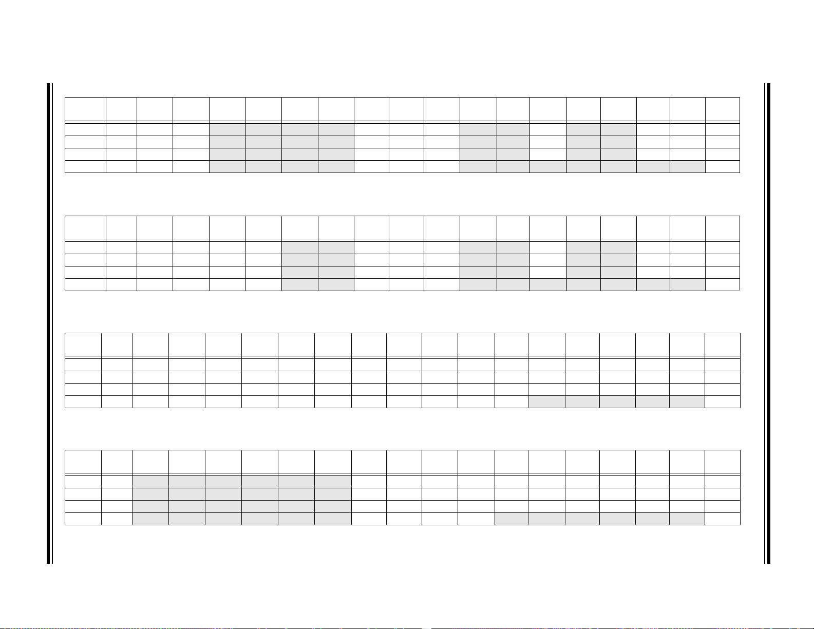
2011-2012 Microchip Technology Inc. DS70652E-page 71
TABLE 4-33: PORTB REGISTER MAP FOR dsPIC33FJ32GP101 DEVICES
File Name Addr Bit 15 Bit 14 Bit 13 Bit 12 Bit 11 Bit 10 Bit 9 Bit 8 Bit 7 Bit 6 Bit 5 Bit 4 Bit 3 Bit 2 Bit 1 Bit 0
TRISB 02C8 TRISB15 TRISB14
PORTB 02CA RB15 RB14
LATB 02CC LATB15 LATB14
ODCB 02CE ODCB15 ODCB14
Legend: x = unknown value on Reset, — = unimplemented, read as ‘0’. Reset values are shown in hexadecimal
— — — — TRISB9 TRISB8 TRISB7 — — TRISB4 — — TRISB1 TRISB0 C393
— — — — RB9 RB8 RB7 — —RB4— —RB1RB0xxxx
— — — — LATB 9 LATB 8 L ATB7 — —LATB4 — —LATB1LATB0xxxx
— — — — ODCB9 ODCB8 ODCB7 — — — — — — — 0000
All
Resets
TABLE 4-34: PORTB REGISTER MAP FOR dsPIC33FJ32MC101 DEVICES
File Name Addr Bit 15 Bit 14 Bit 13 Bit 12 Bit 11 Bit 10 Bit 9 Bit 8 Bit 7 Bit 6 Bit 5 Bit 4 Bit 3 Bit 2 Bit 1 Bit 0
TRISB 02C8 TRISB15 TRISB14 TRISB13 TRISB12
PORTB 02CA RB15 RB14 RB13 RB12
LAT B 02 CC L ATB1 5 L ATB1 4 L ATB1 3 L ATB12
ODCB 02CE ODCB15 ODCB14 ODCB13 ODCB12
Legend: x = unknown value on Reset, — = unimplemented, read as ‘0’. Reset values are shown in hexadecimal
— — TRISB9 TRISB8 TRISB7 — — TRISB4 — — TRISB1 TRISB0 F393
— — RB9 RB8 RB7 — —RB4 — —RB1RB0xxxx
— — L ATB 9 LAT B8 LAT B7 — —LATB4— —LATB1LATB0xxxx
— — ODCB9 ODCB8 ODCB7 — — — — — — — 0000
All
Resets
TABLE 4-35: PORTB REGISTER MAP FOR dsPIC33FJ32(GP/MC)102 AND dsPIC33FJ32(GP/MC)104 DEVICES
File
Name
TRISB 02C8 TRISB15 TRISB14 TRISB13 TRISB12 TRISB11 TRISB10 TRISB9 TRISB8 TRISB7 TRISB6 TRISB5 TRISB4 TRISB3 TRISB2 TRISB1 TRISB0 FFFF
PORTB 02CA RB15 RB14 RB13 RB12 RB11 RB10 RB9 RB8 RB7 RB6 RB5 RB4 RB3 RB2 RB1 RB0 xxxx
LAT B 02 CC L ATB 15 LATB1 4 LATB 13 LAT B12 LAT B11 LAT B10 L ATB9 L ATB8 L ATB7 LATB 6 L ATB5 L ATB4 LAT B3 LAT B2 LAT B1 LAT B0 xxxx
ODCB 02CE ODCB15 ODCB14 ODCB13 ODCB12 ODCB11 ODCB10 ODCB9 ODCB8 ODCB7 ODCB6 ODCB5
Legend: x = unknown value on Reset, — = unimplemented, read as ‘0’. Reset values are shown in hexadecimal.
Addr Bit 15 Bit 14 Bit 13 Bit 12 Bit 11 Bit 10 Bit 9 Bit 8 Bit 7 Bit 6 Bit 5 Bit 4 Bit 3 Bit 2 Bit 1 Bit 0
— — — — — 0000
All
Resets
dsPIC33FJ16(GP/MC)101/102 AND dsPIC33FJ32(GP/MC)101/102/104
TABLE 4-36: PORTC REGISTER MAP FOR dsPIC33FJ32(GP/MC)104 DEVICES
File
Name
TRISC 02D8
PORTC 02DA
LATC 02DC
ODCC 02DE
Legend: x = unknown value on Reset, — = unimplemented, read as ‘0’. Reset values are shown in hexadecimal.
Addr Bit 15 Bit 14 Bit 13 Bit 12 Bit 11 Bit 10 Bit 9 Bit 8 Bit 7 Bit 6 Bit 5 Bit 4 Bit 3 Bit 2 Bit 1 Bit 0
— — — — — — TRISC9 TRISC8 TRISC7 TRISC6 TRISC5 TRISC4 TRISC3 TRISC2 TRISC1 TRISC0 FFFF
— — — — — — RC9 RC8 RC7 RC6 RC5 RC4 RC3 RC2 RC1 RC0 xxxx
— — — — — — L ATC9 LAT C8 LAT C7 LAT C6 L ATC5 LAT C4 L ATC3 LAT C2 LATC 1 L ATC0 xxxx
— — — — — — ODCC9 ODCC8 ODCC7 ODCC6 — — — — — — 0000
All
Resets
DS70652E-page 72 2011-2012 Microchip Technology Inc.
TABLE 4-37: SYSTEM CONTROL REGISTER MAP
File Name Addr Bit 15 Bit 14 Bit 13 Bit 12 Bit 11 Bit 10 Bit 9 Bit 8 Bit 7 Bit 6 Bit 5 Bit 4 Bit 3 Bit 2 Bit 1 Bit 0
RCON 0740 TRAPR IOPUWR
OSCCON 0742 — COSC<2:0> — NOSC<2:0> CLKLOCK IOLOCK LOCK —CF— LPOSCEN OSWEN 0300
CLKDIV 0744 ROI DOZE<2:0> DOZEN FRCDIV<2:0> — — — — — — — — 3040
OSCTUN 0748
Legend: x = unknown value on Reset, — = unimplemented, read as ‘0’. Reset values are shown in hexadecimal.
Note 1: RCON register Reset values are dependent on the type of Reset.
2: OSCCON register Reset values are dependent on the FOSC Configuration bits and by type of Reset.
— — — — — — — — — — TUN<5:0> 0000
— — — — CM VREGS EXTR SWR SWDTEN WDTO SLEEP IDLE BOR POR xxxx
All
Resets
TABLE 4-38: NVM REGISTER MAP
File Name Addr Bit 15 Bit 14 Bit 13 Bit 12 Bit 11 Bit 10 Bit 9 Bit 8 Bit 7 Bit 6 Bit 5 Bit 4 Bit 3 Bit 2 Bit 1 Bit 0
NVMCON 0760 WR WREN WRERR
NVMKEY 0766 — — — — — — — — NVMKEY<7:0> 0000
Legend: x = unknown value on Reset, — = unimplemented, read as ‘0’. Reset values are shown in hexadecimal.
Note 1: Reset value shown is for POR only. Value on other Reset states is dependent on the state of memory write or erase operations at the time of Reset.
— — — — — — ERASE — — NVMOP<3:0> 0000
Resets
TABLE 4-39: PMD REGISTER MAP
File Name Addr Bit 15 Bit 14 Bit 13 Bit 12 Bit 11 Bit 10 Bit 9 Bit 8 Bit 7 Bit 6 Bit 5 Bit 4 Bit 3 Bit 2 Bit 1 Bit 0
PMD1 0770 T5MD
PMD2 0772
PMD3 0774
PMD4 0776
Legend: x = unknown value on Reset, — = unimplemented, read as ‘0’. Reset values are shown in hexadecimal.
Note 1: This bit is available in dsPIC33FJXXMC10X devices only.
2: This bit is available in dsPIC33FJ32(GP/MC)10X devices only.
(2)
— — — — — IC3MD IC2MD IC1MD — — — — — —OC2MDOC1MD0000
— — — — — CMPMD RTCCMD — — — — — — — — — 0000
— — — — — — — — — — — — —CTMUMD— — 0000
T4MD
(2)
T3MD T2MD T1MD —PWM1MD
(1)
— I2C1MD —U1MD— SPI1MD — —AD1MD0000
All
Resets
dsPIC33FJ16(GP/MC)101/102 AND dsPIC33FJ32(GP/MC)101/102/104
(1)
(2)
All
(1)

dsPIC33FJ16(GP/MC)101/102 AND dsPIC33FJ32(GP/MC)101/102/104
<Free Word>
PC<15:0>
000000000
015
W15 (before CALL)
W15 (after CALL)
Stack Grows Toward
Higher Address
0x0000
PC<22:16>
POP : [--W15]
PUSH : [W15++]
4.2.6 SOFTWARE STACK
In addition to its use as a working register, the W15
register in the dsPIC33FJ16(GP/MC)101/102 and
dsPIC33FJ32(GP/MC)101/102/104 devices is also
used as a software Stack Pointer. The Stack Pointer
always points to the first available free word and grows
from lower to higher addresses. It pre-decrements for
stack pops and post-increments for stack pushes, as
shown in Figure 4-6. For a PC push during any CALL
instruction, the MSb of the PC is zero-extended before
the push, ensuring that the MSb is always clear.
Note: A PC push during exception processing
concatenates the SRL register to the MSb
of the PC prior to the push.
The Stack Pointer Limit register (SPLIM) associated
with the Stack Pointer sets an upper address boundary
for the stack. SPLIM is uninitialized at Reset. As is the
case for the Stack Pointer, SPLIM<0> is forced to ‘0’
because all stack operations must be word-aligned.
Whenever an EA is generated using W15 as a source
or destination pointer, the resulting address is
compared with the value in SPLIM. If the contents of
the Stack Pointer (W15) and the SPLIM register are
equal and a push operation is performed, a stack error
trap will not occur. However, the stack error trap will
occur on a subsequent push operation. For example, to
cause a stack error trap when the stack grows beyond
address 0x0C00 in RAM, initialize the SPLIM with the
value 0x0BFE.
Similarly, a Stack Pointer underflow (stack error) trap is
generated when the Stack Pointer address is found to
be less than 0x0800. This prevents the stack from
interfering with the SFR space.
A write to the SPLIM register should not be immediately
followed by an indirect read operation using W15.
FIGURE 4-6: CALL STACK FRAME
4.2.7 DATA RAM PROTECTION FEATURE
The dsPIC33F product family supports Data RAM
protection features that enable segments of RAM to be
protected when used in conjunction with Boot and
Secure Code Segment Security. BSRAM (Secure RAM
Segment for BS) is accessible only from the Boot
Segment Flash code when enabled. SSRAM (Secure
RAM Segment for RAM) is accessible only from the
Secure Segment Flash code when enabled. See
Table 4-1 for an overview of the BSRAM and SSRAM
SFRs.
4.3 Instruction Addressing Modes
The addressing modes shown in Table 4-40 form the
basis of the addressing modes that are optimized to
support the specific features of individual instructions.
The addressing modes provided in the MAC class of
instructions differ from those provided in other
instruction types.
4.3.1 FILE REGISTER INSTRUCTIONS
Most file register instructions use a 13-bit address field
(f) to directly address data present in the first
8192 bytes of data memory (near data space). Most file
register instructions employ a working register, W0,
which is denoted as WREG in these instructions. The
destination is typically either the same file register or
WREG (with the exception of the MUL instruction),
which writes the result to a register or register pair. The
MOV instruction allows additional flexibility and can
access the entire data space.
4.3.2 MCU INSTRUCTIONS
The three-operand MCU instructions are of the form:
Operand 3 = Operand 1 <function> Operand 2
where Operand 1 is always a working register (that is,
the addressing mode can only be register direct), which
is referred to as Wb. Operand 2 can be a W register,
fetched from data memory, or a 5-bit literal. The result
location can be either a W register or a data memory
location. The following addressing modes are
supported by MCU instructions:
• Register Direct
• Register Indirect
• Register Indirect Post-Modified
• Register Indirect Pre-Modified
• 5-Bit or 10-Bit Literal
Note: Not all instructions support all of the
addressing modes given above.
Individual instructions can support
different subsets of these addressing
modes.
2011-2012 Microchip Technology Inc. DS70652E-page 73

dsPIC33FJ16(GP/MC)101/102 AND dsPIC33FJ32(GP/MC)101/102/104
TABLE 4-40: FUNDAMENTAL ADDRESSING MODES SUPPORTED
Addressing Mode Description
File Register Direct The address of the file register is specified explicitly.
Register Direct The contents of a register are accessed directly.
Register Indirect The contents of Wn forms the Effective Address (EA).
Register Indirect Post-Modified The contents of Wn forms the EA. Wn is post-modified (incremented or
decremented) by a constant value.
Register Indirect Pre-Modified Wn is pre-modified (incremented or decremented) by a signed constant value
to form the EA.
Register Indirect with Register Offset
(Register Indexed)
Register Indirect with Literal Offset The sum of Wn and a literal forms the EA.
The sum of Wn and Wb forms the EA.
4.3.3 MOVE AND ACCUMULATOR INSTRUCTIONS
Move instructions and the DSP accumulator class of
instructions provide a greater degree of addressing
flexibility than other instructions. In addition to the
addressing modes supported by most MCU
instructions, move and accumulator instructions also
support Register Indirect with Register Offset
Addressing mode, also referred to as Register Indexed
mode.
Note: For the MOV instructions, the addressing
mode specified in the instruction can differ
for the source and destination EA. However, the 4-bit Wb (Register Offset) field is
shared by both source and destination
(but typically only used by one).
In summary, the following addressing modes are
supported by move and accumulator instructions:
• Register Direct
• Register Indirect
• Register Indirect Post-modified
• Register Indirect Pre-modified
• Register Indirect with Register Offset (Indexed)
• Register Indirect with Literal Offset
• 8-Bit Literal
• 16-Bit Literal
Note: Not all instructions support all the
addressing modes given above. Individual
instructions may support different subsets
of these addressing modes.
4.3.4 MAC INSTRUCTIONS
The dual source operand DSP instructions (CLR, ED,
EDAC, MAC, MPY, MPY.N, MOVSAC, and MSC), also
referred to as MAC instructions, use a simplified set of
addressing modes to allow the user application to
effectively manipulate the Data Pointers through
register indirect tables.
The two-source operand prefetch registers must be
members of the set {W8, W9, W10, W11}. For data
reads, W8 and W9 are always directed to the X RAGU,
and W10 and W11 are always directed to the Y AGU.
The Effective Addresses generated (before and after
modification) must, therefore, be valid addresses within
X data space for W8 and W9 and Y data space for W10
and W11.
Note: Register Indirect with Register Offset
Addressing mode is available only for W9
(in X space) and W11 (in Y space).
In summary, the following addressing modes are
supported by the MAC class of instructions:
• Register Indirect
• Register Indirect Post-Modified by 2
• Register Indirect Post-Modified by 4
• Register Indirect Post-Modified by 6
• Register Indirect with Register Offset (Indexed)
4.3.5 OTHER INSTRUCTIONS
In addition to the addressing modes outlined previously,
some instructions use literal constants of various sizes.
For example, BRA (branch) instructions use 16-bit signed
literals to specify the branch destination directly, whereas
the DISI instruction uses a 14-bit unsigned literal field. In
some instructions, such as ADD Acc, the source of an
operand or result is implied by the opcode itself. Certain
operations, such as NOP, do not have any operands.
DS70652E-page 74 2011-2012 Microchip Technology Inc.

dsPIC33FJ16(GP/MC)101/102 AND dsPIC33FJ32(GP/MC)101/102/104
4.4 Modulo Addressing
Modulo Addressing mode is a method of providing an
automated means to support circular data buffers using
hardware. The objective is to remove the need for
software to perform data address boundary checks
when executing tightly looped code, as is typical in
many DSP algorithms.
Modulo Addressing can operate in either data or program
space (since the Data Pointer mechanism is essentially
the same for both). One circular buffer can be supported
in each of the X (which also provides the pointers into
program space) and Y data spaces. Modulo Addressing
can operate on any W Register Pointer. However, it is not
advisable to use W14 or W15 for Modulo Addressing
since these two registers are used as the Stack Frame
Pointer and Stack Pointer, respectively.
In general, any particular circular buffer can be configured to operate in only one direction as there are
certain restrictions on the buffer start address (for incrementing buffers), or end address (for decrementing
buffers), based upon the direction of the circular buffer.
The only exception to the usage restrictions is for
buffers that have a power-of-two length. As these
buffers satisfy the start and end address criteria, they
can operate in a bidirectional mode (that is, address
boundary checks are performed on both the lower and
upper address boundaries).
4.4.1 START AND END ADDRESS
The Modulo Addressing scheme requires that a
starting and ending address be specified and loaded
into the 16-bit Modulo Buffer Address registers:
XMODSRT, XMODEND, YMODSRT, and YMODEND
(see Ta bl e 4 - 1).
The length of a circular buffer is not directly specified. It
is determined by the difference between the
corresponding start and end addresses. The maximum
possible length of the circular buffer is 32K words
(64 Kbytes).
4.4.2 W ADDRESS REGISTER SELECTION
• The Modulo and Bit-Reversed Addressing Control
register, MODCON<15:0>, contains enable flags
as well as a W register field to specify the W
Address registers. The XWM and YWM fields
select which registers will operate with Modulo
Addressing.
• If XWM = 15, X RAGU and X WAGU Modulo
Addressing is disabled.
• If YWM = 15, Y AGU Modulo Addressing is
disabled.
The X Address Space Pointer W register (XWM), to
which Modulo Addressing is to be applied, is stored in
MODCON<3:0> (see Table 4-1). Modulo Addressing is
enabled for X data space when XWM is set to any value
other than ‘15’ and the XMODEN bit is set at
MODCON<15>.
The Y Address Space Pointer W register (YWM) to
which Modulo Addressing is to be applied is stored in
MODCON<7:4>. Modulo Addressing is enabled for Y
data space when YWM is set to any value other than
‘15’ and the YMODEN bit is set at MODCON<14>.
Note: Y space Modulo Addressing EA calcula-
tions assume word-sized data (LSb of
every EA is always clear).
2011-2012 Microchip Technology Inc. DS70652E-page 75

dsPIC33FJ16(GP/MC)101/102 AND dsPIC33FJ32(GP/MC)101/102/104
0x1100
0x1163
Start Addr = 0x1100
End Addr = 0x1163
Length = 0x0032 Words
Byte
Address
MOV #0x1100, W0
MOV W0, XMODSRT ;set modulo start address
MOV #0x1163, W0
MOV W0, MODEND ;set modulo end address
MOV #0x8001, W0
MOV W0, MODCON ;enable W1, X AGU for modulo
MOV #0x0000, W0 ;W0 holds buffer fill value
MOV #0x1110, W1 ;point W1 to buffer
DO AGAIN, #0x31 ;fill the 50 buffer locations
MOV W0, [W1++] ;fill the next location
AGAIN: INC W0, W0 ;increment the fill value
FIGURE 4-7: MODULO ADDRESSING OPERATION EXAMPLE
DS70652E-page 76 2011-2012 Microchip Technology Inc.

dsPIC33FJ16(GP/MC)101/102 AND dsPIC33FJ32(GP/MC)101/102/104
4.4.3 MODULO ADDRESSING APPLICABILITY
Modulo Addressing can be applied to the Effective
Address (EA) calculation associated with any W
register. Address boundaries check for addresses
equal to:
• The upper boundary addresses for incrementing
buffers
• The lower boundary addresses for decrementing
buffers
It is important to realize that the address boundaries
check for addresses less than or greater than the upper
(for incrementing buffers) and lower (for decrementing
buffers) boundary addresses (not just equal to).
Address changes can, therefore, jump beyond
boundaries and still be adjusted correctly.
Note: The modulo corrected Effective Address
is written back to the register only when
Pre-Modify or Post-Modify Addressing
mode is used to compute the Effective
Address. When an address offset (such
as [W7 + W2]) is used, Modulo Address
correction is performed, but the contents
of the register remain unchanged.
4.5 Bit-Reversed Addressing
Bit-Reversed Addressing mode is intended to simplify
data reordering for radix-2 FFT algorithms. It is
supported by the X AGU for data writes only.
The modifier, which can be a constant value or register
contents, is regarded as having its bit order reversed. The
address source and destination are kept in normal order.
Thus, the only operand requiring reversal is the modifier.
4.5.1 BIT-REVERSED ADDRESSING IMPLEMENTATION
Bit-Reversed Addressing mode is enabled in any of
these situations:
• BWM bits (W register selection) in the MODCON
register are any value other than ‘15’ (the stack
cannot be accessed using Bit-Reversed
Addressing)
• The BREN bit is set in the XBREV register
• The addressing mode used is Register Indirect
with Pre-Increment or Post-Increment
N
If the length of a bit-reversed buffer is M = 2
the last ‘N’ bits of the data buffer start address must
be zeros.
XB<14:0> is the Bit-Reversed Address modifier, or
‘pivot point,’ which is typically a constant. In the case of
an FFT computation, its value is equal to half of the FFT
data buffer size.
Note: All bit-reversed EA calculations assume
word-sized data (LSb of every EA is
always clear). The XB value is scaled
accordingly to generate compatible (byte)
addresses.
When enabled, Bit-Reversed Addressing is executed
only for Register Indirect with Pre-Increment or PostIncrement Addressing and word-sized data writes. It
will not function for any other addressing mode or for
byte-sized data and normal addresses are generated
instead. When Bit-Reversed Addressing is active, the
W Address Pointer is always added to the address
modifier (XB) and the offset associated with the
Register Indirect Addressing mode is ignored. In
addition, as word-sized data is a requirement, the LSb
of the EA is ignored (and always clear).
Note: Modulo Addressing and Bit-Reversed
Addressing should not be enabled
together. If an application attempts to do
so, Bit-Reversed Addressing will assume
priority, when active, for the X WAGU, and
X WAGU, Modulo Addressing will be
disabled. However, Modulo Addressing will
continue to function in the X RAGU.
bytes,
If Bit-Reversed Addressing has already been enabled
by setting the BREN (XBREV<15>) bit, a write to the
XBREV register should not be immediately followed by
an indirect read operation using the W register that has
been designated as the Bit-Reversed Pointer.
2011-2012 Microchip Technology Inc. DS70652E-page 77

dsPIC33FJ16(GP/MC)101/102 AND dsPIC33FJ32(GP/MC)101/102/104
b3 b2 b1 0
b2 b3 b4
0
Bit Locations Swapped Left-to-Right
Around Center of Binary Value
Bit-Reversed Address
XB = 0x0008 for a 16-Word, Bit-Reversed Buffer
b7 b6 b5 b1
b7 b6 b5 b4
b11 b10 b9 b8
b11 b10 b9 b8
b15 b14 b13 b12
b15 b14 b13 b12
Sequential Address
Pivot Point
FIGURE 4-8: BIT-REVERSED ADDRESS EXAMPLE
TABLE 4-41: BIT-REVERSED ADDRESS SEQUENCE (16-ENTRY)
Normal Address Bit-Reversed Address
A3 A2 A1 A0 Decimal A3 A2 A1 A0 Decimal
0000 0 0000 0
0001 1 1000 8
0010 2 0100 4
0011 3 1100 12
0100 4 0010 2
0101 5 1010 10
0110 6 0110 6
0111 7 1110 14
1000 8 0001 1
1001 9 1001 9
1010 10 0101 5
1011 11 1101 13
1100 12 0011 3
1101 13 1011 11
1110 14 0111 7
1111 15 1111 15
DS70652E-page 78 2011-2012 Microchip Technology Inc.

dsPIC33FJ16(GP/MC)101/102 AND dsPIC33FJ32(GP/MC)101/102/104
4.6 Interfacing Program and Data Memory Spaces
The dsPIC33FJ16(GP/MC)101/102 and
dsPIC33FJ32(GP/MC)101/102/104 architecture uses
a 24-bit-wide program space and a 16-bit-wide data
space. The architecture is also a modified Harvard
scheme, meaning that data can also be present in the
program space. To use this data successfully, it must
be accessed in a way that preserves the alignment of
information in both spaces.
Aside from normal execution, the dsPIC33FJ16(GP/
MC)101/102 and dsPIC33FJ32(GP/MC)101/102/104
architecture provides two methods by which program
space can be accessed during operation:
• Using table instructions to access individual
bytes, or words, anywhere in the program space
• Remapping a portion of the program space into
the data space (Program Space Visibility)
Table instructions allow an application to read or write
to small areas of the program memory. This capability
makes the method ideal for accessing data tables that
need to be updated periodically. It also allows access
to all bytes of the program word. The remapping
method allows an application to access a large block of
data on a read-only basis, which is ideal for lookups
from a large table of static data. The application can
only access the lsw of the program word.
4.6.1 ADDRESSING PROGRAM SPACE
Since the address ranges for the data and program
spaces are 16 and 24 bits, respectively, a method is
needed to create a 23-bit or 24-bit program address
from 16-bit data registers. The solution depends on the
interface method to be used.
For table operations, the 8-bit Table Page register
(TBLPAG) is used to define a 32K word region within
the program space. This is concatenated with a 16-bit
EA to arrive at a full 24-bit program space address. In
this format, the MSb of TBLPAG is used to determine if
the operation occurs in the user memory
(TBLPAG<7> = 0) or the configuration memory
(TBLPAG<7> = 1).
For remapping operations, the 8-bit Program Space
Visibility register (PSVPAG) is used to define a
16K word page in the program space. When the MSb
of the EA is ‘1’, PSVPAG is concatenated with the lower
15 bits of the EA to form a 23-bit program space
address. Unlike table operations, this limits remapping
operations strictly to the user memory area.
Table 4-42 and Figure 4-9 show how the program EA is
created for table operations and remapping accesses
from the data EA.
TABLE 4-42: PROGRAM SPACE ADDRESS CONSTRUCTION
Access Type
Instruction Access
(Code Execution)
TBLRD/TBLWT
(Byte/Word Read/Write)
Program Space Visibility
(Block Remap/Read)
Note 1: Data EA<15> is always ‘1’ in this case, but is not used in calculating the program space address. Bit 15 of
the address is PSVPAG<0>.
Access
Space
User 0 PC<22:1> 0
User TBLPAG<7:0> Data EA<15:0>
Configuration TBLPAG<7:0> Data EA<15:0>
User 0 PSVPAG<7:0> Data EA<14:0>
<23> <22:16> <15> <14:1> <0>
0xx xxxx xxxx xxxx xxxx xxx0
0xxx xxxx xxxx xxxx xxxx xxxx
1xxx xxxx xxxx xxxx xxxx xxxx
0 xxxx xxxx xxx xxxx xxxx xxxx
Program Space Address
(1)
2011-2012 Microchip Technology Inc. DS70652E-page 79
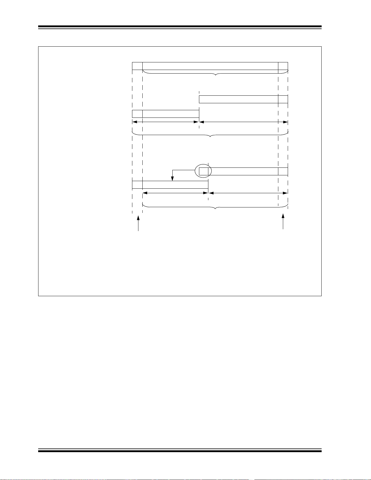
dsPIC33FJ16(GP/MC)101/102 AND dsPIC33FJ32(GP/MC)101/102/104
0
Program Counter
23 Bits
1
PSVPAG
8 Bits
EA
15 Bits
Program Counter
(1)
Select
TBLPAG
8 Bits
EA
16 Bits
Byte Select
0
0
1/0
User/Configuration
Table Operations
(2)
Program Space Visibility
(1)
Space Select
24 Bits
23 Bits
(Remapping)
1/0
0
Note 1: The Least Significant bit of program space addresses is always fixed as ‘0’ to maintain word
alignment of data in the program and data spaces.
2: Table operations are not required to be word-aligned. Table read operations are permitted
in the configuration memory space.
FIGURE 4-9: DATA ACCESS FROM PROGRAM SPACE ADDRESS GENERATION
DS70652E-page 80 2011-2012 Microchip Technology Inc.

dsPIC33FJ16(GP/MC)101/102 AND dsPIC33FJ32(GP/MC)101/102/104
081623
00000000
00000000
00000000
00000000
‘Phantom’ Byte
TBLRDH.B (Wn<0> = 0)
TBLRDL.W
TBLRDL.B (Wn<0> = 1)
TBLRDL.B (Wn<0> = 0)
23 15 0
TBLPAG
02
0x000000
0x800000
0x020000
0x030000
Program Space
The address for the table operation is determined by the data EA
within the page defined by the TBLPAG register.
Only read operations are shown; write operations are also valid in
the user memory area.
4.6.2 DATA ACCESS FROM PROGRAM
MEMORY USING TABLE
INSTRUCTIONS
The TBLRDL and TBLWTL instructions offer a direct
method of reading or writing the lower word of any
address within the program space without going
through data space. The TBLRDH and TBLWTH
instructions are the only method to read or write the
upper 8 bits of a program space word as data.
The PC is incremented by two for each successive
24-bit program word. This allows program memory
addresses to directly map to data space addresses. Program memory can thus be regarded as two 16-bit-wide
word address spaces, residing side by side, each with
the same address range. TBLRDL and TBLWTL access
the space that contains the least significant data word.
TBLRDH and TBLWTH access the space that contains the
upper data byte.
Two table instructions are provided to move byte or
word-sized (16-bit) data to and from program space.
Both function as either byte or word operations.
• TBLRDL (Table Read Low):
- In Word mode, this instruction maps the
lower word of the program space location
(P<15:0>) to a data address (D<15:0>).
- In Byte mode, either the upper or lower byte
of the lower program word is mapped to the
lower byte of a data address. The upper byte
is selected when Byte Select is ‘1’; the lower
byte is selected when it is ‘0’.
• TBLRDH (Table Read High):
- In Word mode, this instruction maps the entire
upper word of a program address (P<23:16>)
to a data address. Note that D<15:8>, the
‘phantom byte’, will always be ‘0’.
- In Byte mode, this instruction maps the upper
or lower byte of the program word to D<7:0>
of the data address, in the TBLRDL instruc-
tion. The data is always ‘0’ when the upper
‘phantom’ byte is selected (Byte Select = 1).
In a similar fashion, two table instructions, TBLWTH
and TBLWTL, are used to write individual bytes or
words to a program space address. The details of
their operation are explained in Section 5.0 “Flash
Program Memory”.
For all table operations, the area of program memory
space to be accessed is determined by the Table Page
register (TBLPAG). TBLPAG covers the entire program
memory space of the device, including user and
configuration spaces. When TBLPAG<7> = 0, the table
page is located in the user memory space. When
TBLPAG<7> = 1, the page is located in configuration
space.
FIGURE 4-10: ACCESSING PROGRAM MEMORY WITH TABLE INSTRUCTIONS
2011-2012 Microchip Technology Inc. DS70652E-page 81

dsPIC33FJ16(GP/MC)101/102 AND dsPIC33FJ32(GP/MC)101/102/104
23 15 0
PSVPAG
Data Space
Program Space
0x0000
0x8000
0xFFFF
02
0x000000
0x800000
0x010000
0x018000
When CORCON<2> = 1 and EA<15> = 1:
The data in the page
designated by
PSVPAG is mapped
into the upper half of
the data memory
space...
Data EA<14:0>
...while the lower 15 bits
of the EA specify an
exact address within
the PSV area. This
corresponds exactly to
the same lower 15 bits
of the actual program
space address.
PSV Area
4.6.3 READING DATA FROM PROGRAM MEMORY USING PROGRAM SPACE VISIBILITY
The upper 32 Kbytes of data space may optionally be
mapped into any 16K word page of the program space.
This option provides transparent access to stored
constant data from the data space without the need to
use special instructions (such as TBLRDL and
TBLRDH).
Program space access through the data space occurs
if the MSb of the data space EA is ‘1’ and program
space visibility is enabled by setting the PSV bit in the
Core Control register (CORCON<2>). The location of
the program memory space to be mapped into the data
space is determined by the Program Space Visibility
Page register (PSVPAG). This 8-bit register defines
any one of 256 possible pages of 16K words in
program space. In effect, PSVPAG functions as the
upper 8 bits of the program memory address, with the
15 bits of the EA functioning as the lower bits. By
incrementing the PC by 2 for each program memory
word, the lower 15 bits of data space addresses directly
map to the lower 15 bits in the corresponding program
space addresses.
Data reads to this area add a cycle to the instruction
being executed, since two program memory fetches
are required.
Although each data space address, 0x8000 and higher,
maps directly into a corresponding program memory
address (see Figure 4-11), only the lower 16 bits of the
24-bit program word are used to contain the data. The
upper 8 bits of any program space location used as
data should be programmed with ‘1111 1111’ or
‘0000 0000’ to force a NOP. This prevents possible
issues should the area of code ever be accidentally
executed.
Note: PSV access is temporarily disabled during
table reads/writes.
For operations that use PSV and are executed outside
a REPEAT loop, the MOV and MOV.D instructions
require one instruction cycle in addition to the specified
execution time. All other instructions require two
instruction cycles in addition to the specified execution
time.
For operations that use PSV, and are executed inside
a REPEAT loop, these instances require two instruction
cycles in addition to the specified execution time of the
instruction:
• Execution in the first iteration
• Execution in the last iteration
• Execution prior to exiting the loop due to an
interrupt
• Execution upon re-entering the loop after an
interrupt is serviced
Any other iteration of the REPEAT loop will allow the
instruction using PSV to access data, to execute in a
single cycle.
FIGURE 4-11: PROGRAM SPACE VISIBILITY OPERATION
DS70652E-page 82 2011-2012 Microchip Technology Inc.

dsPIC33FJ16(GP/MC)101/102 AND dsPIC33FJ32(GP/MC)101/102/104
0
Program Counter
24 Bits
Program Counter
TBLPAG Reg
8 Bits
Working Reg EA
16 Bits
Byte
24-Bit EA
0
1/0
Select
Using
Table Instruction
Using
User/Configuration
Space Select
5.0 FLASH PROGRAM MEMORY
Note 1: This data sheet summarizes the features
of the dsPIC33FJ16(GP/MC)101/102 and
dsPIC33FJ32(GP/MC)101/102/104 family
devices. It is not intended to be a
comprehensive reference source. To
complement the information in this data
sheet, refer to Section 5. “Flash
Programming” (DS70191) in the
“dsPIC33F/PIC24H Family Reference
Manual”, which is available from the
Microchip web site (www.microchip.com).
2: Some registers and associated bits
described in this section may not be
available on all devices. Refer to
Section 4.0 “Memory Organization” in
this data sheet for device-specific register
and bit information.
The dsPIC33FJ16(GP/MC)101/102 and
dsPIC33FJ32(GP/MC)101/102/104 devices contain
internal Flash program memory for storing and
executing application code. The memory is readable,
writable, and erasable during normal operation over the
entire V
Flash memory can be programmed in two ways:
• In-Circuit Serial Programming™ (ICSP™)
• Run-Time Self-Programming (RTSP)
DD range.
programming capability
ICSP allows a device to be serially programmed while
in the end application circuit. This is done with two lines
for programming clock and programming data (one of
the alternate programming pin pairs: PGECx/PGEDx),
and three other lines for power (V
DD), ground (VSS) and
Master Clear (MCLR). This allows users to manufacture boards with unprogrammed devices, and then
program the Digital Signal Controller just before
shipping the product. This also allows the most recent
firmware or a custom firmware to be programmed.
RTSP is accomplished using TBLRD (table read) and
TBLWT (table write) instructions. With RTSP, the user
application can write program memory data in a single
program memory word, and erase program memory in
blocks or ‘pages’ of 512 instructions (1536 bytes).
5.1 Table Instructions and Flash
Programming
Regardless of the method used, all programming of
Flash memory is done with the table read and table
write instructions. These allow direct read and write
access to the program memory space, from the data
memory, while the device is in normal operating mode.
The 24-bit target address in the program memory is
formed using bits <7:0> of the TBLPAG register and the
Effective Address (EA) from a W register specified in
the table instruction, as shown in Figure 5-1.
The TBLRDL and the TBLWTL instructions are used to
read or write to bits<15:0> of program memory.
TBLRDL and TBLWTL can access program memory in
both Word and Byte modes.
The TBLRDH and TBLWTH instructions are used to read
or write to bits <23:16> of program memory. TBLRDH
and TBLWTH can also access program memory in Word
or Byte mode.
FIGURE 5-1: ADDRESSING FOR TABLE REGISTERS
2011-2012 Microchip Technology Inc. DS70652E-page 83

dsPIC33FJ16(GP/MC)101/102 AND dsPIC33FJ32(GP/MC)101/102/104
T
7.37 MHz FRC Accuracy% FRC Tuning%
--------------------------------------------------------------------------------------------------------------------------
T
RW
355 Cycles
7.37 MHz 10.02+1 0.00375–
----------------------------------------------------------------------------------------------
47.4s==
T
RW
355 Cycles
7.37 MHz 10.02–1 0.00375–
----------------------------------------------------------------------------------------------
49.3s==
5.2 RTSP Operation
The dsPIC33FJ16(GP/MC)101/102 and
dsPIC33FJ32(GP/MC)101/102/104 Flash program
memory array is organized into rows of 64 instructions or
192 bytes. RTSP allows the user application to erase a
page of memory, which consists of eight rows
(512 instructions); and to program one word. Table 26-12
shows typical erase and programming times. The 8-row
erase pages are edge-aligned from the beginning of
program memory, on boundaries of 1536 bytes.
5.3 Programming Operations
A complete programming sequence is necessary for
programming or erasing the internal Flash in RTSP
mode. The processor stalls (waits) until the operation is
finished.
The programming time depends on the FRC accuracy
(see Table 26-18) and the value of the FRC Oscillator
Tuning register (see Register 8-3). Use the following
formula to calculate the minimum and maximum values
for the Word Write Time and Page Erase Time (see
Table 26-12).
EQUATION 5-1: PROGRAMMING TIME
5.3.1 PROGRAMMING ALGORITHM FOR
FLASH PROGRAM MEMORY
Programmers can program one word (24 bits) of
program Flash memory at a time. To do this, it is
necessary to erase the 8-row erase page that contains
the desired address of the location the user wants to
change.
For protection against accidental operations, the write
initiate sequence for NVMKEY must be used to allow
any erase or program operation to proceed. After the
programming command has been executed, the user
application must wait for the programming time until
programming is complete. The two instructions
following the start of the programming sequence
should be NOPs.
Note: Performing a page erase operation on the
last page of program memory will clear the
Flash Configuration Words, thereby
enabling code protection as a result.
Therefore, users should avoid performing
page erase operations on the last page of
program memory.
Refer to Section 5. “Flash Programming” (DS70191)
in the “dsPIC33F/PIC24H Family Reference Manual”
for details and codes examples on programming using
RTSP.
For example, if the device is operating at +125°C, the
FRC accuracy will be ±2%. If the TUN<5:0> bits (see
Register 8-3) are set to ‘b000000, the minimum row
write time is equal to Equation 5-2.
EQUATION 5-2: MINIMUM ROW WRITE
TIME
The maximum row write time is equal to Equation 5-3.
EQUATION 5-3: MAXIMUM ROW WRITE
TIME
Setting the WR bit (NVMCON<15>) starts the operation, and the WR bit is automatically cleared when the
operation is finished.
5.4 Control Registers
Two SFRs are used to read and write the program
Flash memory: NVMCON and NVMKEY.
The NVMCON register (Register 5-1) controls which
blocks are to be erased, which memory type is to be
programmed, and the start of the programming cycle.
NVMKEY is a write-only register that is used for write
protection. To start a programming or erase sequence,
the user application must consecutively write 0x55 and
0xAA to the NVMKEY register. Refer to Section 5.3
“Programming Operations” for further details.
DS70652E-page 84 2011-2012 Microchip Technology Inc.
dsPIC33FJ16(GP/MC)101/102 AND dsPIC33FJ32(GP/MC)101/102/104
REGISTER 5-1: NVMCON: FLASH MEMORY CONTROL REGISTER
(1)
R/SO-0
WR WREN WRERR
bit 15 bit 8
R/W-0
(1)
R/W-0
(1)
U-0 U-0 U-0 U-0 U-0
— — — — —
U-0 R/W-0
(1)
U-0 U-0 R/W-0
— ERASE — —NVMOP<3:0>
(1)
R/W-0
(1)
R/W-0
(2)
(1)
R/W-0
(1)
bit 7 bit 0
Legend: SO = Settable Only bit
R = Readable bit W = Writable bit U = Unimplemented bit, read as ‘0’
-n = Value at POR ‘1’ = Bit is set ‘0’ = Bit is cleared x = Bit is unknown
bit 15 WR: Write Control bit
(1)
1 = Initiates a Flash memory program or erase operation. The operation is self-timed and the bit is
cleared by hardware once operation is complete
0 = Program or erase operation is complete and inactive
bit 14 WREN: Write Enable bit
(1)
1 = Enables Flash program/erase operations
0 = Inhibits Flash program/erase operations
bit 13 WRERR: Write Sequence Error Flag bit
(1)
1 = An improper program or erase sequence attempt or termination has occurred (bit is set automatically
on any set attempt of the WR bit)
0 = The program or erase operation completed normally
bit 12-7 Unimplemented: Read as ‘0’
bit 6 ERASE: Erase/Program Enable bit
(1)
1 = Performs the erase operation specified by NVMOP<3:0> on the next WR command
0 = Performs the program operation specified by NVMOP<3:0> on the next WR command
bit 5-4 Unimplemented: Read as ‘0’
bit 3-0 NVMOP<3:0>: NVM Operation Select bits
(1,2)
If ERASE = 1:
1111 = No operation
1101 = Erase General Segment
1100 = No operation
0011 = No operation
0010 = Memory page erase operation
0001 = No operation
0000 = No operation
If ERASE =
0:
1111 = No operation
1101 = No operation
1100 = No operation
0011 = Memory word program operation
0010 = No operation
0001 = No operation
0000 = No operation
Note 1: These bits can only be reset on a POR.
2: All other combinations of NVMOP<3:0> are unimplemented.
2011-2012 Microchip Technology Inc. DS70652E-page 85

dsPIC33FJ16(GP/MC)101/102 AND dsPIC33FJ32(GP/MC)101/102/104
REGISTER 5-2: NVMKEY: NONVOLATILE MEMORY KEY REGISTER
U-0 U-0 U-0 U-0 U-0 U-0 U-0 U-0
— — — — — — — —
bit 15 bit 8
W-0 W-0 W-0 W-0 W-0 W-0 W-0 W-0
NVMKEY<7:0>
bit 7 bit 0
Legend:
R = Readable bit W = Writable bit U = Unimplemented bit, read as ‘0’
-n = Value at POR ‘1’ = Bit is set ‘0’ = Bit is cleared x = Bit is unknown
bit 15-8 Unimplemented: Read as ‘0’
bit 7-0 NVMKEY<7:0>: Key Register bits (write-only)
DS70652E-page 86 2011-2012 Microchip Technology Inc.

dsPIC33FJ16(GP/MC)101/102 AND dsPIC33FJ32(GP/MC)101/102/104
MCLR
VDD
BOR
Sleep or Idle
RESET Instruction
WDT
Module
Glitch Filter
Trap Conflict
Illegal Opcode
Uninitialized W Register
SYSRST
VDD Rise
Detect
POR
Configuration Mismatch
Internal
Regulator
6.0 RESETS
Note 1: This data sheet summarizes the features
of the dsPIC33FJ16(GP/MC)101/102
and dsPIC33FJ32(GP/MC)101/102/104
family devices. It is not intended to be a
comprehensive reference source. To
complement the information in this data
sheet, refer to Section 8. “Reset”
(DS70192) in the “dsPIC33F/PIC24H
Family Reference Manual”, which is
available from the Microchip web site
(www.microchip.com).
2: Some registers and associated bits
described in this section may not be
available on all devices. Refer to
Section 4.0 “Memory Organization” in
this data sheet for device-specific register
and bit information.
The Reset module combines all Reset sources and
controls the device Master Reset Signal, SYSRST
following is a list of device Reset sources:
• POR: Power-on Reset
• BOR: Brown-out Reset
•MCLR
: Master Clear Pin Reset
•SWR: RESET Instruction
• WDTO: Watchdog Timer Reset
• CM: Configuration Mismatch Reset
• TRAPR: Trap Conflict Reset
• IOPUWR: Illegal Condition Device Reset
- Illegal Opcode Reset
- Uninitialized W Register Reset
- Security Reset
. The
A simplified block diagram of the Reset module is
shown in Figure 6-1.
Any active source of Reset will make the SYSRST
signal active. On system Reset, some of the registers
associated with the CPU and peripherals are forced to
a known Reset state, and some are unaffected.
Note: Refer to the specific peripheral section or
Section 3.0 “CPU” of this data sheet for
register Reset states.
All types of device Reset set a corresponding status bit
in the RCON register to indicate the type of Reset (see
Register 6-1).
All bits that are set, with the exception of the POR bit
(RCON<0>), are cleared during a POR event. The user
application can set or clear any bit at any time during
code execution. The RCON bits only serve as status
bits. Setting a particular Reset status bit in software
does not cause a device Reset to occur.
The RCON register also has other bits associated with
the Watchdog Timer and device power-saving states.
The function of these bits is discussed in other sections
of this data sheet.
Note: The status bits in the RCON register
should be cleared after they are read so
that the next RCON register value after a
device Reset is meaningful.
FIGURE 6-1: RESET SYSTEM BLOCK DIAGRAM
2011-2012 Microchip Technology Inc. DS70652E-page 87
dsPIC33FJ16(GP/MC)101/102 AND dsPIC33FJ32(GP/MC)101/102/104
6.1 Reset Control Register
REGISTER 6-1: RCON: RESET CONTROL REGISTER
R/W-0 R/W-0 U-0 U-0 U-0 U-0 R/W-0 R/W-0
TRAPR IOPUWR — — — —CMVREGS
bit 15 bit 8
R/W-0 R/W-0 R/W-0 R/W-0 R/W-0 R/W-0 R/W-1 R/W-1
EXTR SWR SWDTEN
bit 7 bit 0
Legend:
R = Readable bit W = Writable bit U = Unimplemented bit, read as ‘0’
-n = Value at POR ‘1’ = Bit is set ‘0’ = Bit is cleared x = Bit is unknown
bit 15 TRAPR: Trap Reset Flag bit
1 = A Trap Conflict Reset has occurred
0 = A Trap Conflict Reset has not occurred
bit 14 IOPUWR: Illegal Opcode or Uninitialized W Access Reset Flag bit
1 = An illegal opcode detection, an illegal address mode or uninitialized W register used as an
Address Pointer caused a Reset
0 = An Illegal Opcode or Uninitialized W Reset has not occurred
bit 13-10 Unimplemented: Read as ‘0’
bit 9 CM: Configuration Mismatch Flag bit
1 = A Configuration Mismatch Reset has occurred
0 = A Configuration Mismatch Reset has not occurred
bit 8 VREGS: Voltage Regulator Stand-by During Sleep bit
1 = Voltage regulator is active during Sleep
0 = Voltage regulator goes into Stand-by mode during Sleep
bit 7 EXTR: External Reset (MCLR) Pin bit
1 = A Master Clear (pin) Reset has occurred
0 = A Master Clear (pin) Reset has not occurred
bit 6 SWR: Software Reset (Instruction) Flag bit
1 = A RESET instruction has been executed
0 = A RESET instruction has not been executed
bit 5 SWDTEN: Software Enable/Disable of WDT bit
1 = WDT is enabled
0 = WDT is disabled
bit 4 WDTO: Watchdog Timer Time-out Flag bit
1 = WDT time-out has occurred
0 = WDT time-out has not occurred
bit 3 SLEEP: Wake-up from Sleep Flag bit
1 = Device has been in Sleep mode
0 = Device has not been in Sleep mode
(2)
WDTO SLEEP IDLE BOR POR
(1)
(2)
Note 1: All of the Reset status bits can be set or cleared in software. Setting one of these bits in software does not
cause a device Reset.
2: If the FWDTEN Configuration bit is ‘1’ (unprogrammed), the WDT is always enabled, regardless of the
SWDTEN bit setting.
DS70652E-page 88 2011-2012 Microchip Technology Inc.

dsPIC33FJ16(GP/MC)101/102 AND dsPIC33FJ32(GP/MC)101/102/104
REGISTER 6-1: RCON: RESET CONTROL REGISTER
bit 2 IDLE: Wake-up from Idle Flag bit
1 = Device has been in Idle mode
0 = Device has not been in Idle mode
bit 1 BOR: Brown-out Reset Flag bit
1 = A Brown-out Reset has occurred
0 = A Brown-out Reset has not occurred
bit 0 POR: Power-on Reset Flag bit
1 = A Power-on Reset has occurred
0 = A Power-on Reset has not occurred
Note 1: All of the Reset status bits can be set or cleared in software. Setting one of these bits in software does not
cause a device Reset.
2: If the FWDTEN Configuration bit is ‘1’ (unprogrammed), the WDT is always enabled, regardless of the
SWDTEN bit setting.
(1)
(CONTINUED)
2011-2012 Microchip Technology Inc. DS70652E-page 89

dsPIC33FJ16(GP/MC)101/102 AND dsPIC33FJ32(GP/MC)101/102/104
6.2 System Reset
The dsPIC33FJ16(GP/MC)101/102 and
dsPIC33FJ32(GP/MC)101/102/104 family of devices
have two types of Reset:
• Cold Reset
• Warm Reset
A Cold Reset is the result of a POR or a BOR. On a
Cold Reset, the FNOSC Configuration bits in the FOSC
Configuration register selects the device clock source.
A Warm Reset is the result of all other Reset sources,
including the RESET instruction. On Warm Reset, the
device will continue to operate from the current clock
source as indicated by the Current Oscillator Selection (COSC<2:0>) bits in the Oscillator Control
(OSCCON<14:12>) register.
The device is kept in a Reset state until the system
power supplies have stabilized at appropriate levels
and the oscillator clock is ready. The sequence in
which this occurs is shown in Figure 6-2.
TABLE 6-1: OSCILLATOR DELAY
Oscillator Mode
FRC, FRCDIV16,
Oscillator
Start-up Delay
(1)
OSCD
T
FRCDIVN
FRCPLL TOSCD
MS TOSCD
HS TOSCD
(1)
(1)
(1)
EC — — — —
MSPLL T
OSCD
(1)
ECPLL — — TLOCK
SOSC TOSCD
LPRC TOSCD
(1)
(1)
Note 1: TOSCD = Oscillator Start-up Delay (1.1 s max. for FRC, 70 s max. for LPRC). Crystal oscillator start-up
times vary with crystal characteristics, load capacitance, etc.
OST = Oscillator Start-up Timer Delay (1024 oscillator clock period). For example, TOST = 102.4 s for a
2: T
10 MHz crystal and TOST = 32 ms for a 32 kHz crystal.
LOCK = PLL Lock time (1.5 ms nominal) if PLL is enabled.
3: T
Oscillator Start-up
Timer
—— TOSCD
—TLOCK
(2)
TOST
(2)
TOST
(2)
TOST
(2)
TOST
—— TOSCD
PLL Lock Time Total Delay
(3)
—TOSCD
—TOSCD
(3)
TLOCK
(3)
TOSCD
—TOSCD
TOSCD
(1)
+ TOST
(1)
+ TLOCK
(1)
+ TOST
(1)
+ TOST
TLOCK
(1)
+ TOST
(2)
+ TLOCK
(3)
(1)
(3)
(2)
(2)
(2)
(3)
DS70652E-page 90 2011-2012 Microchip Technology Inc.

dsPIC33FJ16(GP/MC)101/102 AND dsPIC33FJ32(GP/MC)101/102/104
Reset
Run
Device Status
V
DD
VPOR
VBOR
POR
BOR
SYSRST
TPWRT
TPOR
TBOR
Oscillator Clock
T
OSCD TOST TLOCK
Time
FSCM
T
FSCM
1
2
3
4
5
6
1. POR: A POR circuit holds the device in Reset when the power supply is turned on. The POR circuit is active until V
DD crosses the
V
POR threshold and the delay, TPOR, has elapsed.
2. BOR: The on-chip voltage regulator has a BOR circuit that keeps the device in Reset until V
DD crosses the VBOR threshold and the
delay, T
BOR, has elapsed. The delay, TBOR, ensures the voltage regulator output becomes stable.
3. PWRT Timer: The Power-up Timer continues to hold the processor in Reset for a specific period of time (T
PWRT) after a BOR. The
delay, T
PWRT, ensures that the system power supplies have stabilized at the appropriate level for full-speed operation. After the delay,
T
PWRT, has elapsed, the SYSRST becomes inactive, which in turn, enables the selected oscillator to start generating clock cycles.
4. Oscillator Delay: The total delay for the clock to be ready for various clock source selections is given in Table 6-1. Refer to
Section 8.0 “Oscillator Configuration” for more information.
5. When the oscillator clock is ready, the processor begins execution from location, 0x000000. The user application programs a GOTO
instruction at the Reset address, which redirects program execution to the appropriate start-up routine.
6. The Fail-Safe Clock Monitor (FSCM), if enabled, begins to monitor the system clock when the system clock is ready and the delay,
T
FSCM, has elapsed.
FIGURE 6-2: SYSTEM RESET TIMING
TABLE 6-2: OSCILLATOR PARAMETERS
Symbol Parameter Value
V
POR POR Threshold 1.8V nominal
T
POR POR Extension Time 30 s maximum
V
BOR BOR Threshold 2.5V nominal
BOR BOR Extension Time 100 s maximum
T
T
PWRT Power-up Time
Delay
TFSCM Fail-Safe Clock
Monitor Delay
64 ms nominal
900 s maximum
Note: When the device exits the Reset condition
(begins normal operation), the device
operating parameters (voltage, frequency,
temperature, etc.) must be within their
operating ranges; otherwise, the device
may not function correctly. The user application must ensure that the delay between
the time power is first applied, and the time
SYSRST
becomes inactive, is long
enough to get all operating parameters
within specification.
2011-2012 Microchip Technology Inc. DS70652E-page 91
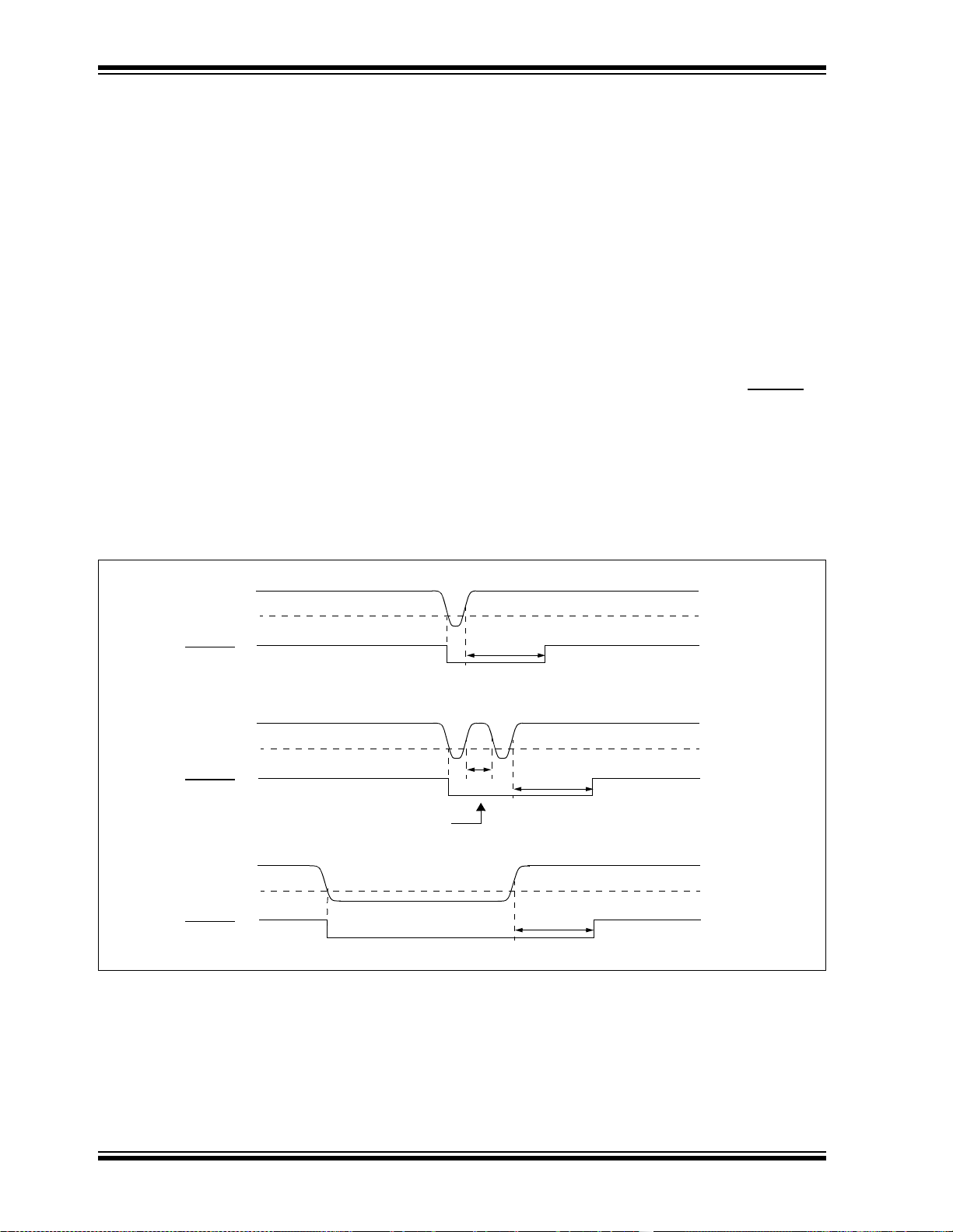
dsPIC33FJ16(GP/MC)101/102 AND dsPIC33FJ32(GP/MC)101/102/104
VDD
SYSRST
VBOR
V
DD
SYSRST
VBOR
V
DD
SYSRST
VBOR
T
BOR
+ T
PWRT
VDD Dips Before PWRT Expires
T
BOR
+ T
PWRT
T
BOR
+ T
PWRT
6.3 POR
A POR circuit ensures the device is reset from poweron. The POR circuit is active until V
VPOR threshold and the delay, TPOR, has elapsed. The
delay, TPOR, ensures that the internal device bias
circuits become stable.
The device supply voltage characteristics must meet
the specified starting voltage and rise rate requirements to generate the POR. Refer to Section 26.0
“Electrical Characteristics” for details.
The POR status (POR) bit in the Reset Control
(RCON<0>) register is set to indicate the Power-on
Reset.
FIGURE 6-3: BROWN-OUT RESET SITUATIONS
DD crosses the
6.4 BOR and PWRT
The on-chip regulator has a BOR circuit that resets the
device when the V
device operation. The BOR circuit keeps the device in
Reset until VDD crosses the VBOR threshold and the
delay, T
BOR, has elapsed. The delay, TBOR, ensures
the voltage regulator output becomes stable.
The BOR status (BOR) bit in the Reset Control
(RCON<1>) register is set to indicate the Brown-out
Reset.
The device will not run at full speed after a BOR as the
DD should rise to acceptable levels for full-speed
V
operation. The Power-up Timer (PWRT) provides
power-up time delay (T
power supplies have stabilized at the appropriate levels
for full-speed operation before the SYSRST
released.
Refer to Section 23.0 “Special Features” for further
details.
Figure 6-3 shows the typical brown-out scenarios. The
Reset delay (T
rises above the VBOR trip point.
DD is too low (VDD < VBOR) for proper
PWRT) to ensure that the system
is
BOR + TPWRT) is initiated each time VDD
DS70652E-page 92 2011-2012 Microchip Technology Inc.

dsPIC33FJ16(GP/MC)101/102 AND dsPIC33FJ32(GP/MC)101/102/104
6.5 External Reset (EXTR)
The External Reset is generated by driving the MCLR
pin low. The MCLR pin is a Schmitt trigger input with an
additional glitch filter. Reset pulses that are longer than
the minimum pulse width will generate a Reset. Refer
to Section 26.0 “Electrical Characteristics” for
minimum pulse-width specifications. The External
Reset (MCLR
(RCON) register is set to indicate the MCLR Reset.
6.5.1 EXTERNAL SUPERVISORY
Many systems have external supervisory circuits that
generate Reset signals to reset multiple devices in the
system. This External Reset signal can be directly connected to the MCLR
rest of the system is reset.
6.5.2 INTERNAL SUPERVISORY CIRCUIT
When using the internal power supervisory circuit to
reset the device, the External Reset pin (MCLR
be tied directly or resistively to VDD. In this case, the
MCLR pin will not be used to generate a Reset. The
External Reset pin (MCLR
pull-up and must not be left unconnected.
) Pin (EXTR) bit in the Reset Control
CIRCUIT
pin to reset the device when the
) should
) does not have an internal
6.8 Trap Conflict Reset
If a lower priority hard trap occurs while a higher priority
trap is being processed, a hard Trap Conflict Reset
occurs. The hard traps include exceptions of Priority
Level 13 through Level 15, inclusive. The address error
(Level 13) and oscillator error (Level 14) traps fall into
this category.
The Trap Reset Flag (TRAPR) bit in the Reset Control
(RCON<15>) register is set to indicate the Trap Conflict
Reset. Refer to Section 7.0 “Interrupt Controller” for
more information on Trap Conflict Resets.
6.9 Configuration Mismatch Reset
To maintain the integrity of the Peripheral Pin Select
Control registers, they are constantly monitored with
shadow registers in hardware. If an unexpected
change in any of the registers occurs (such as cell
disturbances caused by ESD or other external events),
a Configuration Mismatch Reset occurs.
The Configuration Mismatch Flag (CM) bit in the Reset
Control (RCON<9>) register is set to indicate the
Configuration Mismatch Reset. Refer to Section 10.0
“I/O Ports” for more information on the Configuration
Mismatch Reset.
6.6 Software RESET Instruction (SWR)
Whenever the RESET instruction is executed, the device
will assert SYSRST, placing the device in a special
Reset state. This Reset state will not re-initialize the
clock. The clock source in effect prior to the RESET
instruction will remain as the source. SYSRST
released at the next instruction cycle and the Reset
vector fetch will commence.
The Software Reset (Instruction) Flag (SWR) bit in the
Reset Control (RCON<6>) register is set to indicate the
Software Reset.
is
6.7 Watchdog Timer Time-out Reset (WDTO)
Whenever a Watchdog Timer Time-out Reset occurs,
the device will asynchronously assert SYSRST
clock source will remain unchanged. A WDT time-out
during Sleep or Idle mode will wake-up the processor,
but will not reset the processor.
The Watchdog Timer Time-out Flag (WDTO) bit in the
Reset Control (RCON<4>) register is set to indicate the
Watchdog Reset. Refer to Section 23.4 “Watchdog
Timer (WDT)” for more information on Watchdog
Reset.
. The
Note: The Configuration Mismatch feature and
associated Reset flag is not available on
all devices.
6.10 Illegal Condition Device Reset
An Illegal Condition Device Reset occurs due to the
following sources:
• Illegal Opcode Reset
• Uninitialized W Register Reset
• Security Reset
The Illegal Opcode or Uninitialized W Access Reset
Flag (IOPUWR) bit in the Reset Control (RCON<14>)
register is set to indicate the Illegal Condition Device
Reset.
6.10.1 ILLEGAL OPCODE RESET
A device Reset is generated if the device attempts to
execute an illegal opcode value that is fetched from
program memory.
The Illegal Opcode Reset function can prevent the
device from executing program memory sections that
are used to store constant data. To take advantage of
the Illegal Opcode Reset, use only the lower 16 bits of
each program memory section to store the data values.
The upper 8 bits should be programmed with 0x3F,
which is an illegal opcode value.
2011-2012 Microchip Technology Inc. DS70652E-page 93

dsPIC33FJ16(GP/MC)101/102 AND dsPIC33FJ32(GP/MC)101/102/104
6.10.2 UNINITIALIZED W REGISTER RESET
Any attempts to use the uninitialized W register as an
Address Pointer will reset the device. The W register
array (with the exception of W15) is cleared during all
Resets and is considered uninitialized until written to.
6.10.3 SECURITY RESET
If a Program Flow Change (PFC) or Vector Flow
Change (VFC) targets a restricted location in a
protected segment (Boot and Secure Segment), that
operation will cause a Security Reset.
The PFC occurs when the Program Counter is
reloaded as a result of a Call, Jump, Computed Jump,
Return, Return from Subroutine or other form of branch
instruction.
The VFC occurs when the Program Counter is
reloaded with an interrupt or trap vector.
6.11 Using the RCON Status Bits
The user application can read the Reset Control
(RCON) register after any device Reset to determine
the cause of the Reset.
Note: The status bits in the RCON register
should be cleared after they are read so
that the next RCON register value after a
device Reset will be meaningful.
Table 6-3 provides a summary of Reset flag bit
operation.
TABLE 6-3: RESET FLAG BIT OPERATION
Flag Bit Set by: Cleared by:
TRAPR (RCON<15>) Trap conflict event POR, BOR
IOPWR (RCON<14>) Illegal opcode or uninitialized
W register access or Security Reset
CM (RCON<9>) Configuration Mismatch POR, BOR
EXTR (RCON<7>) MCLR
SWR (RCON<6>) RESET instruction POR, BOR
WDTO (RCON<4>) WDT Time-out PWRSAV instruction,
SLEEP (RCON<3>) PWRSAV #SLEEP instruction POR, BOR
IDLE (RCON<2>) PWRSAV #IDLE instruction POR, BOR
BOR (RCON<1>) POR, BOR —
POR (RCON<0>) POR —
Note: All Reset flag bits can be set or cleared by user software.
Reset POR
POR, BOR
CLRWDT instruction, POR, BOR
DS70652E-page 94 2011-2012 Microchip Technology Inc.

dsPIC33FJ16(GP/MC)101/102 AND dsPIC33FJ32(GP/MC)101/102/104
7.0 INTERRUPT CONTROLLER
Note 1: This data sheet summarizes the features
of the dsPIC33FJ16(GP/MC)101/102
and dsPIC33FJ32(GP/MC)101/102/104
family devices. It is not intended to be a
comprehensive reference source. To
complement the information in this data
sheet, refer to Section 41. “Interrupts
(Part IV)” (DS70300) in the “dsPIC33F/
PIC24H Family Reference Manual”,
which is available on the Microchip web
site (www.microchip.com).
2: Some registers and associated bits
described in this section may not be
available on all devices. Refer to
Section 4.0 “Memory Organization” in
this data sheet for device-specific register
and bit information.
The interrupt controller reduces the numerous peripheral interrupt request signals to a single interrupt
request signal to the dsPIC33FJ16(GP/MC)101/102
and dsPIC33FJ32(GP/MC)101/102/104 CPU. It has
the following features:
• Up to eight processor exceptions and software traps
• Seven user-selectable priority levels
• Interrupt Vector Table (IVT) with up to 118 vectors
• A unique vector for each interrupt or exception
source
• Fixed priority within a specified user priority level
• Alternate Interrupt Vector Table (AIVT) for debug
support
• Fixed interrupt entry and return latencies
7.1 Interrupt Vector Table
The Interrupt Vector Table (IVT) is shown in Figure 7-1.
The IVT resides in program memory, starting at location,
000004h. The IVT contains 126 vectors consisting of
eight non-maskable trap vectors, plus up to 118 sources
of interrupt. In general, each interrupt source has its own
vector. Each interrupt vector contains a 24-bit-wide
address. The value programmed into each interrupt
vector location is the starting address of the associated
Interrupt Service Routine (ISR).
Interrupt vectors are prioritized in terms of their natural
priority. This priority is linked to their position in the
vector table. Lower addresses generally have a higher
natural priority. For example, the interrupt associated
with Vector 0 will take priority over interrupts at any
other vector address.
dsPIC33FJ16(GP/MC)101/102 and dsPIC33FJ32(GP/
MC)101/102/104 devices implement up to 26 unique
interrupts and 4 nonmaskable traps. These are
summarized in Ta bl e 7 - 1 and Table 7-2.
7.1.1 ALTERNATE INTERRUPT VECTOR TA BL E
The Alternate Interrupt Vector Table (AIVT) is located
after the IVT, as shown in Figure 7-1. Access to the
AIVT is provided by the ALTIVT control bit
(INTCON2<15>). If the ALTIVT bit is set, all interrupt
and exception processes use the alternate vectors
instead of the default vectors. The alternate vectors are
organized in the same manner as the default vectors.
The AIVT supports debugging by providing a way to
switch between an application and a support environment without requiring the interrupt vectors to be
reprogrammed. This feature also enables switching
between applications to facilitate evaluation of different
software algorithms at run time. If the AIVT is not
needed, the AIVT should be programmed with the
same addresses used in the IVT.
7.2 Reset Sequence
A device Reset is not a true exception because the interrupt controller is not involved in the Reset process. The
dsPIC33FJ16(GP/MC)101/102 and dsPIC33FJ32(GP/
MC)101/102/104 devices clear their registers in
response to a Reset, forcing the PC to zero. The Digital
Signal Controller then begins program execution at
location, 0x000000. A GOTO instruction at the Reset
address can redirect program execution to the
appropriate start-up routine.
Note: Any unimplemented or unused vector
locations in the IVT and AIVT should be
programmed with the address of a default
interrupt handler routine that contains a
RESET instruction.
2011-2012 Microchip Technology Inc. DS70652E-page 95

dsPIC33FJ16(GP/MC)101/102 AND dsPIC33FJ32(GP/MC)101/102/104
Reset – GOTO Instruction 0x000000
Reset – GOTO Address 0x000002
Reserved 0x000004
Oscillator Fail Trap Vector
Address Error Trap Vector
Stack Error Trap Vector
Math Error Trap Vector
Reserved
Reserved
Reserved
Interrupt Vector 0 0x000014
Interrupt Vector 1
~
~
~
Interrupt Vector 52 0x00007C
Interrupt Vector 53 0x00007E
Interrupt Vector 54 0x000080
~
~
~
Interrupt Vector 116 0x0000FC
Interrupt Vector 117 0x0000FE
Reserved
0x000100
Reserved 0x000102
Reserved
Oscillator Fail Trap Vector
Address Error Trap Vector
Stack Error Trap Vector
Math Error Trap Vector
Reserved
Reserved
Reserved
Interrupt Vector 0 0x000114
Interrupt Vector 1
~
~
~
Interrupt Vector 52 0x00017C
Interrupt Vector 53 0x00017E
Interrupt Vector 54 0x000180
~
~
~
Interrupt Vector 116
Interrupt Vector 117 0x0001FE
Start of Code 0x000200
Decreasing Natural Order Priority
Interrupt Vector Table (IVT)
(1)
Alternate Interrupt Vector Table (AIVT)
(1)
Note 1: See Table 7-1 for the list of implemented interrupt vectors.
FIGURE 7-1: dsPIC33FJ16(GP/MC)101/102 AND dsPIC33FJ32(GP/MC)101/102/104
INTERRUPT VECTOR TABLE
DS70652E-page 96 2011-2012 Microchip Technology Inc.

dsPIC33FJ16(GP/MC)101/102 AND dsPIC33FJ32(GP/MC)101/102/104
TABLE 7-1: INTERRUPT VECTORS
Vector
Number
8 0 0x000014 0x000114 INT0 – External Interrupt 0
9 1 0x000016 0x000116 IC1 – Input Capture 1
10 2 0x000018 0x000118 OC1 – Output Compare 1
11 3 0x00001A 0x00011A T1 – Timer1
12 4 0x00001C 0x00011C Reserved
13 5 0x00001E 0x00011E IC2 – Input Capture 2
14 6 0x000020 0x000120 OC2 – Output Compare 2
15 7 0x000022 0x000122 T2 – Timer2
16 8 0x000024 0x000124 T3 – Timer3
17 9 0x000026 0x000126 SPI1E – SPI1 Error
18 10 0x000028 0x000128 SPI1 – SPI1 Transfer Done
19 11 0x00002A 0x00012A U1RX – UART1 Receiver
20 12 0x00002C 0x00012C U1TX – UART1 Transmitter
21 13 0x00002E 0x00012E ADC1 – ADC1
22-23 14-15 0x000030-0x000032 0x000130-0x000132 Reserved
24 16 0x000034 0x000134 SI2C1 – I2C1 Slave Events
25 17 0x000036 0x000136 MI2C1 – I2C1 Master Events
26 18 0x000038 0x000138 CMP – Comparator Interrupt
27 19 0x00003A 0x00013A Change Notification Interrupt
28 20 0x00003C 0x00013C INT1 – External Interrupt 1
29-34 21-26 0x00003E-0x000038 0x00013E-0x000138 Reserved
35 27 0x00004A 0x00014A T4 – Timer4
36 28 0x00004C 0x00014C T5 – Timer4
37 29 0x00004E 0x00014E INT2 – External Interrupt 2
38-44 30-36 0x000050-0x00005C 0x000150-0x00015C Reserved
45 37 0x00005E 0x00015E IC3 – Input Capture 3
46-64 38-56 0x000060-0x000084 0x000160-0x000184 Reserved
65 57 0x000086 0x000186 PWM1 – PWM1 Period Match
66-69 58-61 0x000088-0x00008E 0x000188-0x00018E Reserved
70 62 0x000090 0x000190 RTCC – Real-Time Clock and Calendar
71 63 0x000092 0x000192 FLTA1
72 64 0x000094 0x000194 FLTB1 – PWM1 Fault B
73 65 0x000096 0x000196 U1E – UART1 Error
74-84 66-76 0x000098-0x0000AC 0x000198-0x0001AC Reserved
85 77 0x0000AE 0x0001AE CTMU – Charge Time Measurement Unit
86-125 78-117 0x0000B0-0x0000FE 0x0001B0-0x0001FE Reserved
Note 1: This interrupt vector is available in dsPIC33FJ(16/32)MC10X devices only.
Interrupt
Request (IRQ)
IVT Address AIVT Address Interrupt Source
Number
(2)
(2)
– PWM1 Fault A
2: This interrupt vector is available in dsPIC33FJ32(GP/MC)10X devices only.
3: This interrupt vector is available in dsPIC33FJ(16/32)MC102/104 devices only.
(1)
(1)
(3)
2011-2012 Microchip Technology Inc. DS70652E-page 97

dsPIC33FJ16(GP/MC)101/102 AND dsPIC33FJ32(GP/MC)101/102/104
TABLE 7-2: TRAP VECTORS
Vector Number IVT Address AIVT Address Trap Source
0 0x000004 0x000104 Reserved
1 0x000006 0x000106 Oscillator Failure
2 0x000008 0x000108 Address Error
3 0x00000A 0x00010A Stack Error
4 0x00000C 0x00010C Math Error
5 0x00000E 0x00010E Reserved
6 0x000010 0x000110 Reserved
7 0x000012 0x000112 Reserved
7.3 Interrupt Control and Status Registers
The dsPIC33FJ16(GP/MC)101/102 and
dsPIC33FJ32(GP/MC)101/102/104 devices implement
a total of 22 registers for the interrupt controller:
• INTCON1
• INTCON2
•IFSx
•IECx
•IPCx
•INTTREG
7.3.1 INTCON1 AND INTCON2
Global interrupt functions are controlled from INTCON1
and INTCON2. INTCON1 contains the Interrupt Nesting Disable (NSTDIS) bit as well as the control and
status flags for the processor trap sources. The
INTCON2 register controls the external interrupt
request signal behavior and the use of the Alternate
Interrupt Vector Table.
7.3.2 IFSx Registers
The IFSx registers maintain all of the interrupt request
flags. Each source of interrupt has a status bit, which is
set by the respective peripherals or external signal and
is cleared via software.
7.3.3 IECx Registers
The IECx registers maintain all of the interrupt enable
bits. These control bits are used to individually enable
interrupts from the peripherals or external signals.
7.3.4 IPCx Registers
The IPCx registers are used to set the Interrupt Priority
Level (IPL) for each source of interrupt. Each user
interrupt source can be assigned to one of eight priority
levels.
7.3.5 INTTREG
The INTTREG register contains the associated
interrupt vector number and the new CPU Interrupt
Priority Level, which are latched into Vector Number
(VECNUM<6:0>) and Interrupt Level (ILR<3:0>) bit
fields in the INTTREG register. The new Interrupt
Priority Level is the priority of the pending interrupt.
The interrupt sources are assigned to the IFSx, IECx
and IPCx registers in the same sequence that they are
listed in Ta bl e 7 - 1. For example, the INT0 (External
Interrupt 0) is shown as having Vector Number 8 and a
natural order priority of 0. Thus, the INT0IF bit is found
in IFS0<0>, the INT0IE bit in IEC0<0> and the INT0IPx
bits in the first positions of IPC0 (IPC0<2:0>).
7.3.6 STATUS/CONTROL REGISTERS
Although they are not specifically part of the interrupt
control hardware, two of the CPU Control registers
contain bits that control interrupt functionality.
• The CPU STATUS Register, SR, contains the
IPL<2:0> bits (SR<7:5>). These bits indicate the
current CPU Interrupt Priority Level. The user
application can change the current CPU Interrupt
Priority Level by writing to the IPLx bits.
• The CORCON register contains the IPL3 bit
which, together with IPL<2:0>, also indicates the
current CPU Interrupt Priority Level. IPL3 is a
read-only bit so that trap events cannot be
masked by the user software.
All Interrupt registers are described in Register 7-1
through Register 7-28 in the following pages.
DS70652E-page 98 2011-2012 Microchip Technology Inc.
dsPIC33FJ16(GP/MC)101/102 AND dsPIC33FJ32(GP/MC)101/102/104
REGISTER 7-1: SR: CPU STATUS REGISTER
(1)
R-0 R-0 R/C-0 R/C-0 R-0 R/C-0 R-0 R/W-0
OA OB SA SB OAB SAB DA DC
bit 15 bit 8
R/W-0
IPL2
(3)
(2)
R/W-0
IPL1
(2)
(3)
R/W-0
IPL0
(2)
(3)
R-0 R/W-0 R/W-0 R/W-0 R/W-0
RA N OV Z C
bit 7 bit 0
Legend: C = Clearable bit
R = Readable bit W = Writable bit U = Unimplemented bit, read as ‘0’
-n = Value at POR ‘1’ = Bit is set ‘0’ = Bit is cleared x = Bit is unknown
bit 7-5 IPL<2:0>: CPU Interrupt Priority Level Status bits
(2,3)
111 = CPU Interrupt Priority Level is 7 (15); user interrupts are disabled
110 = CPU Interrupt Priority Level is 6 (14)
101 = CPU Interrupt Priority Level is 5 (13)
100 = CPU Interrupt Priority Level is 4 (12)
011 = CPU Interrupt Priority Level is 3 (11)
010 = CPU Interrupt Priority Level is 2 (10)
001 = CPU Interrupt Priority Level is 1 (9)
000 = CPU Interrupt Priority Level is 0 (8)
Note 1: For complete register details, see Register 3-1.
2: The IPL<2:0> bits are concatenated with the IPL<3> bit (CORCON<3>) to form the CPU Interrupt Priority
Level. The value in parentheses indicates the IPL if IPL<3> = 1. User interrupts are disabled when
IPL<3> = 1.
3: The IPL<2:0> Status bits are read-only when NSTDIS (INTCON1<15>) = 1.
REGISTER 7-2: CORCON: CORE CONTROL REGISTER
(1)
U-0 U-0 U-0 R/W-0 R/W-0 R-0 R-0 R-0
— — —USEDT DL<2:0>
bit 15 bit 8
R/W-0 R/W-0 R/W-1 R/W-0 R/C-0 R/W-0 R/W-0 R/W-0
SATA SATB SATDW ACCSAT IPL3
(2)
PSV RND IF
bit 7 bit 0
Legend: C = Clearable bit
R = Readable bit W = Writable bit U = Unimplemented bit, read as ‘0’
-n = Value at POR ‘1’ = Bit is set ‘0’ = Bit is cleared x = Bit is unknown
bit 3 IPL3: CPU Interrupt Priority Level Status bit 3
(2)
1 = CPU Interrupt Priority Level is greater than 7
0 = CPU Interrupt Priority Level is 7 or less
Note 1: For complete register details, see Register 3-2.
2: The IPL3 bit is concatenated with the IPL<2:0> bits (SR<7:5>) to form the CPU Interrupt Priority Level.
2011-2012 Microchip Technology Inc. DS70652E-page 99

dsPIC33FJ16(GP/MC)101/102 AND dsPIC33FJ32(GP/MC)101/102/104
REGISTER 7-3: INTCON1: INTERRUPT CONTROL REGISTER 1
R/W-0 R/W-0 R/W-0 R/W-0 R/W-0 R/W-0 R/W-0 R/W-0
NSTDIS OVAERR OVBERR COVAERR COVBERR OVATE OVBTE COVTE
bit 15 bit 8
R/W-0 R/W-0 U-0 R/W-0 R/W-0 R/W-0 R/W-0 U-0
SFTACERR DIV0ERR
bit 7 bit 0
Legend:
R = Readable bit W = Writable bit U = Unimplemented bit, read as ‘0’
-n = Value at POR ‘1’ = Bit is set ‘0’ = Bit is cleared x = Bit is unknown
bit 15 NSTDIS: Interrupt Nesting Disable bit
1 = Interrupt nesting is disabled
0 = Interrupt nesting is enabled
bit 14 OVAERR: Accumulator A Overflow Trap Flag bit
1 = Trap was caused by overflow of Accumulator A
0 = Trap was not caused by overflow of Accumulator A
bit 13 OVBERR: Accumulator B Overflow Trap Flag bit
1 = Trap was caused by overflow of Accumulator B
0 = Trap was not caused by overflow of Accumulator B
bit 12 COVAERR: Accumulator A Catastrophic Overflow Trap Flag bit
1 = Trap was caused by catastrophic overflow of Accumulator A
0 = Trap was not caused by catastrophic overflow of Accumulator A
bit 11 COVBERR: Accumulator B Catastrophic Overflow Trap Flag bit
1 = Trap was caused by catastrophic overflow of Accumulator B
0 = Trap was not caused by catastrophic overflow of Accumulator B
bit 10 OVATE: Accumulator A Overflow Trap Enable bit
1 = Trap overflow of Accumulator A
0 = Trap is disabled
bit 9 OVBTE: Accumulator B Overflow Trap Enable bit
1 = Trap overflow of Accumulator B
0 = Trap disabled
bit 8 COVTE: Catastrophic Overflow Trap Enable bit
1 = Trap on catastrophic overflow of Accumulator A or B enabled
0 = Trap is disabled
bit 7 SFTACERR: Shift Accumulator Error Status bit
1 = Math error trap was caused by an invalid accumulator shift
0 = Math error trap was not caused by an invalid accumulator shift
bit 6 DIV0ERR: Arithmetic Error Status bit
1 = Math error trap was caused by a divide-by-zero
0 = Math error trap was not caused by a divide-by-zero
bit 5 Unimplemented: Read as ‘0’
bit 4 MATHERR: Arithmetic Error Status bit
1 = Math error trap has occurred
0 = Math error trap has not occurred
— MATHERR ADDRERR STKERR OSCFAIL —
DS70652E-page 100 2011-2012 Microchip Technology Inc.
 Loading...